

Page 1
123 Rad-Hard MSI Logic
UT54ACS191/UT54ACTS191
Radiation-Hardened
Synchronous 4-Bit Up-Down Binary Counters
FEATURES
Single down/up count control line
counters
Fully synchronous in count modes
Asynchronously presetable with load control
radiation-hardened CMOS
High speed
Low power consumption
Single 5 volt supply
Available QML Q or V processes
Flexible package
- 16-pin DIP
- 16-lead flatpack
DESCRIPTION
The UT54ACS191 and the UT54ACTS191 are synchronous 4bit reversible up-down binary counters. Synchronous counting
operation is provided by having all flip-flops clocked simultaneously so that the outputs change coincident with each other
when so instructed. Synchronous operation eliminates the output counting spikes associated with asynchronous counters.
The outputs of the four flip-flops are triggered on a low-to-highlevel transition of the clock input if the enable input (CTEN) is
low. A logic one applied to CTEN inhibits counting. The direction of the count is determined by the level of the down/up
(D/U) input. When D/U is low, the counter counts up and when
D/U is high, it counts down.
The counters feature a fully independent clock circuit. Changes
at control inputs (CTEN and D/U) that will modify the operating
mode have no effect on the contents of the counter until clocking
occurs.
The counters are fully programmable. The outputs may be
preset to either logic level by placing a low on the load input
and entering the desired data at the data inputs. The output will
change to agree with the data inputs independently of the level
of the clock input. The asynchronous load allows counters to
be used as modulo-N dividers by simply modifying the count
length with the preset inputs.
Two outputs have been made available to perform the cascading
function: ripple clock and maximum/minimum (MAX/MIN)
count. The MAX/MIN output produces a high-level output
pulse with a duration approximately equal to one complete cycle
of the clock while the count is zero (all outputs low) counting
down or maximum (15) counting up.
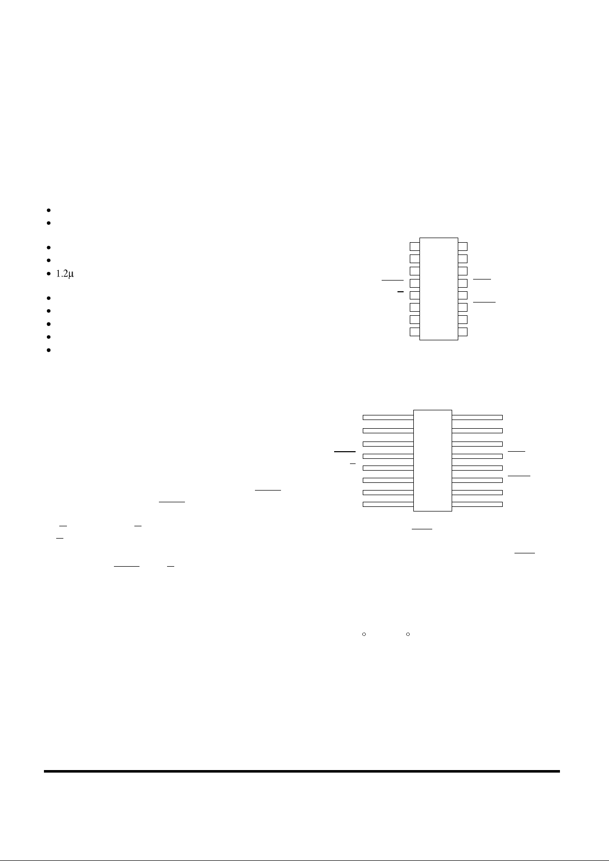
PINOUTS
16-Pin DIP
Top View
16-Lead Flatpack
Top View
The ripple clock output (RCO) produces a low-level output
pulse under those same conditions but only while the clock input
is low. The counters easily cascade by feeding the RCO to the
enable input of the succeeding counter if parallel clocking is
used, or to the clock input if parallel enabling is used. Use the
MAX/MIN count output to accomplish look-ahead for highspeed operation.
The devices are characterized over full military temperature
range of -55 C to +125
1
3
5
6
15
13
10
B
B
A
D/
Q
Q
V
A
RCO
C
9
SS
LOAD
2
4
7
16
14
12
11
DD
9
Q
Q
CTEN
U
C
D
CLK
MAX/MIN
C
SS
Page 2
Rad-Hard MSI Logic 124
UT54ACS191/UT54ACTS191
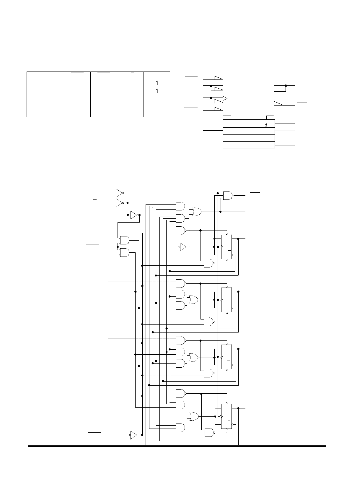
FUNCTION TABLE LOGIC SYMBOL
LOGIC DIAGRAM
FUNCTION LOAD CTEN D/U CLK
Count Up H L L
Count Down H L H
Asynchronous
Reset
L X X X
No Change H H X X
(4)
CTEN
(5)
D/U
M3 (UP)
G1
CTRDIV 16
(14)
CLK
(15)
A
(1)
B
(10)
C
(9)
D
(12)
MAX/MIN
(3)
Q
A
(7)
Q
D
1,2 -/1,3+
(6)
Q
C
(2)
Q
B
5D
(1)
(2)
(4)
(8)
2(CT=0)Z6
M2 (DWN)
G4
3(CT=9)Z6
(11)
LOAD C5
(13)
RCO
6,1,4
7
Note:
1. Logic symbol in accordance with ANSI/IEEE standard 91-1984 and IEC
Publication 617-12.
CLK
D/U
CTEN
LOAD
(11)
(9)
(10)
(1)
(4)
S
R
1J
C1
1K
(7)
(6)
(2)
(3)
(13)
(12)
Q
D
Q
C
Q
B
Q
A
MAX/MIN
RCO
A
B
C
D
(15)
(5)
(14)
S
R
1J
C1
1K
S
R
1J
C1
1K
R
1J
C1
1K
S
Q
Q
Q
Q
Q
Q
Q
Q
Page 3

125 Rad-Hard MSI Logic
UT54ACS191/UT54ACTS191
RADIATION HARDNESS SPECIFICATIONS
1
Notes:
1. Logic will not latchup during radiation exposure within the limits defined in the table.
2. Device storage elements are immune to SEU affects.
ABSOLUTE MAXIMUM RATINGS
Note:
1. Stresses outside the listed absolute maximum ratings may cause permanent damage to the device. This is a stress rating only, functional operation of the device
at these or any other conditions beyond limits indicated in the operational sections is not recommended. Exposure to absolute maximum rating conditions for
extended periods may affect device reliability.
RECOMMENDED OPERATING CONDITIONS
PARAMETER LIMIT UNITS
Total Dose 1.0E6 rads(Si)
SEU Threshold
2
80
MeV-cm2/mg
SEL Threshold 120
MeV-cm2/mg
Neutron Fluence 1.0E14
n/cm
2
SYMBOL PARAMETER LIMIT UNITS
V
DD
Supply voltage -0.3 to 7.0 V
V
I/O
Voltage any pin -.3 to VDD +.3 V
T
STG
Storage Temperature range -65 to +150 C
T
J
Maximum junction temperature +175 C
T
LS
Lead temperature (soldering 5 seconds) +300 C
JC
Thermal resistance junction to case 20 C/W
I
I
DC input current 10 mA
P
D
Maximum power dissipation 1 W
SYMBOL PARAMETER LIMIT UNITS
V
DD
Supply voltage 4.5 to 5.5 V
V
IN
Input voltage any pin 0 to V
DD
V
T
C
Temperature range -55 to + 125 C
Page 4

Rad-Hard MSI Logic 126
UT54ACS191/UT54ACTS191
DC ELECTRICAL CHARACTERISTICS
7
(VDD = 5.0V 10%; VSS = 0V 6, -55 C < TC < +125 C)
SYMBOL PARAMETER CONDITION MIN MAX UNIT
V
IL
Low-level input voltage
1
ACTS
ACS
0.8
.3V
DD
V
V
IH
High-level input voltage
1
ACTS
ACS
.5V
DD
.7V
DD
V
I
IN
Input leakage current
ACTS/ACS VIN = V
DD
or V
SS
-1
1 A
V
OL
Low-level output voltage
3
ACTS
ACS
I
OL
= 8.0mA
I
OL
= 100 A
0.40
0.25
V
V
OH
High-level output voltage
3
ACTS
ACS
I
OH
= -8.0mA
I
OH
= -100 A
.7V
DD
VDD - 0.25
V
I
OS
Short-circuit output current
2 ,4
ACTS/ACS
VO = VDD and V
SS
-200 200 mA
I
OL Output current
10
(Sink)
VIN = VDD or V
SS
VOL = 0.4V
8 mA
I
OH
Output current
10
(Source)
VIN = VDD or V
SS
VOH = VDD - 0.4V
-8 mA
P
total
Power dissipation
2, 8, 9
CL = 50pF 2.1 mW/
MHz
I
DDQ
Quiescent Supply Current VDD = 5.5V 10 A
I
DDQ
Quiescent Supply Current Delta
ACTS
For input under test
VIN = VDD - 2.1V
For all other inputs
VIN = VDD or V
SS
V
DD
= 5.5V
1.6 mA
C
IN
Input capacitance
5
= 1MHz @ 0V 15 pF
C
OUT
Output capacitance 5
= 1MHz @ 0V 15 pF
Page 5

127 Rad-Hard MSI Logic
UT54ACS191/UT54ACTS191
Notes:
1. Functional tests are conducted in accordance with MIL-STD-883 with the following input test conditions: VIH = VIH(min) + 20%, - 0%; VIL = VIL(max) + 0%,
- 50%, as specified herein, for TTL, CMOS, or Schmitt compatible inputs. Devices may be tested using any input voltage within the above specified range, but
are guaranteed to VIH(min) and VIL(max).
2. Supplied as a design limit but not guaranteed or tested.
3. Per MIL-PRF-38535, for current density 5.0E5 amps/cm2, the maximum product of load capacitance (per output buffer) times frequency should not exceed
3,765 pF/MHz.
4. Not more than one output may be shorted at a time for maximum duration of one second.
5. Capacitance measured for initial qualification and when design changes may affect the value. Capacitance is measured between the designated terminal and VSS
at frequency of 1MHz and a signal amplitude of 50mV rms maximum.
6. Maximum allowable relative shift equals 50mV.
7. All specifications valid for radiation dose 1E6 rads(Si).
8. Power does not include power contribution of any TTL output sink current.
9. Power dissipation specified per switching output.
10. This value is guaranteed based on characterization data, but not tested.
Page 6

Rad-Hard MSI Logic 128
UT54ACS191/UT54ACTS191
AC ELECTRICAL CHARACTERISTICS
2
(VDD = 5.0V 10%; VSS = 0V 1, -55 C < TC < +125 C)
Notes:
1. Maximum allowable relative shift equals 50mV.
2. All specifications valid for radiation dose 1E6 rads(Si).
3. Based on characterization, hold time (tH2) of 0ns can be assumed if data setup time (t
SU2
) is >10ns. This is guaranteed, but not tested.
SYMBOL PARAMETER MINIMUM MAXIMUM UNIT
t
PLH
LOAD to Q
n
2 20 ns
t
PHL
LOAD to Q
n
2 22 ns
t
PLH
Data In to Q
n
2 23 ns
t
PHL
Data In to Q
n
2 19 ns
t
PLH
CLK to Q
n
2 17 ns
t
PHL
CLK to Q
n
2 22 ns
t
PLH
CLK to RCO 2 12 ns
t
PHL
CLK to RCO 2 15 ns
t
PLH
CLK to MAX/MIN 2 22 ns
t
PHL
CLK to MAX/MIN 2 23 ns
t
PLH
D/U to RCO 2 16 ns
t
PHL
D/U to RCO 2 18 ns
t
PLH
D/U to MAX/MIN 2 15 ns
t
PHL
D/U to MAX/MIN 2 17 ns
t
PLH
CTEN to RCO 2 12 ns
t
PHL
CTEN to RCO 2 16 ns
f
MAX
Maximum clock frequency 63 MHz
t
SU1
LOAD , CTEN, D/U
Setup time before CLK
12 ns
t
SU2
A, B, C, D setup time before LOAD 5 ns
t
H1
CTEN and D/U hold time after CLK 2 ns
t
H2
3
A, B, C, D hold time after LOAD 2 ns
t
W
Minimum pulse width
CLK high
CLK low
LOAD low
8 ns
 Loading...