

Page 1
113 RadHard MSI Logic
UT54ACS165/UT54ACTS165
Radiation-Hardened
8-Bit Parallel Shift Registers
FEATURES
Complementary outputs
Direct overriding load (data) inputs
Gated clock inputs
Parallel-to-serial data conversions
radiation-hardened CMOS
- Latchup immune
High speed
Low power consumption
Single 5 volt supply
Available QML Q or V processes
Flexible package
- 16-pin DIP
- 16-lead flatpack
DESCRIPTION
The UT54ACS165 and the UT54ACTS165 are 8-bit serial shift registers that, when clocked, shift the data toward serial output QH. Parallel-
in access to each stage is provided by eight individual data inputs that
are enabled by a low level at the SH/LD input. The devices feature a
clock inhibit function and a complemented serial output QH .
Clocking is accomplished by a low-to-high transition of the CLK input
while SH/LD is held high and CLK INH is held low. The functions of
the CLK and CLK INH (clock inhibit) inputs are interchangeable.
Since a low CLK input and a low-to-high transition of CLK INH will
also accomplish clocking, CLK INH should be changed to the high
level only while the CLK input is high. Parallel loading is disabled
when SH/LD is held high. Parallel inputs to the registers are enabled
while SH/LD is low independently of the levels of CLK, CLK INH or
SER inputs.
The devices are characterized over full military temperature range of
-55 C to +125 C.
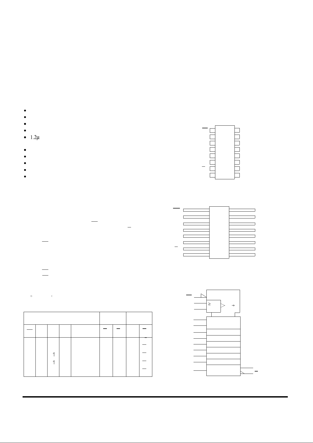
FUNCTION TABLE
Note:
1. Qn = The state of the referenced output one setup time prior to the Low-toHigh clock transition.
PINOUTS
16-Pin DIP
Top View
16-Lead Flatpack
Top View
LOGIC SYMBOL
INPUTS INTERNAL
OUTPUTS
OUTPUTS
SH/LDCLK
INH
CLK SER PARALLEL
A . . . H
QAQBQHQ
H
L X X X a . . . h a b h
h
H L L X X QAQBQHQ
H
H L H X H QAQGQ
G
H L L X L QAQGQ
G
H H X X X QAQBQHQ
H
1
2
3
4
5
7
6
16
15
14
13
12
10
11
SH/LD
CLK
E
F
G
H
Q
H
V
DD
CLK INH
D
C
B
A
SER
8
9
V
SS
Q
H
1
2
3
4
5
7
6
16
15
14
13
12
10
11
V
DD
8 9
SH/LD
CLK
E
F
G
H
Q
H
CLK INH
D
C
B
A
SER
V
SS
Q
H
(1)
SH/LD
(15)
CLK INH
C2/
C1 (LOAD)
(10)
SER
(11)
A
SRG8
(9)
Q
H
(7)
Q
H
1
(2)
CLK
2D
1D
(12)
B
(13)
C
(14)
D
(3)
E
(4)
F
(5)
G
(6)
H
1D
1D
Page 2
RadHard MSI Logic 114
UT54ACS165/UT54ACTS165
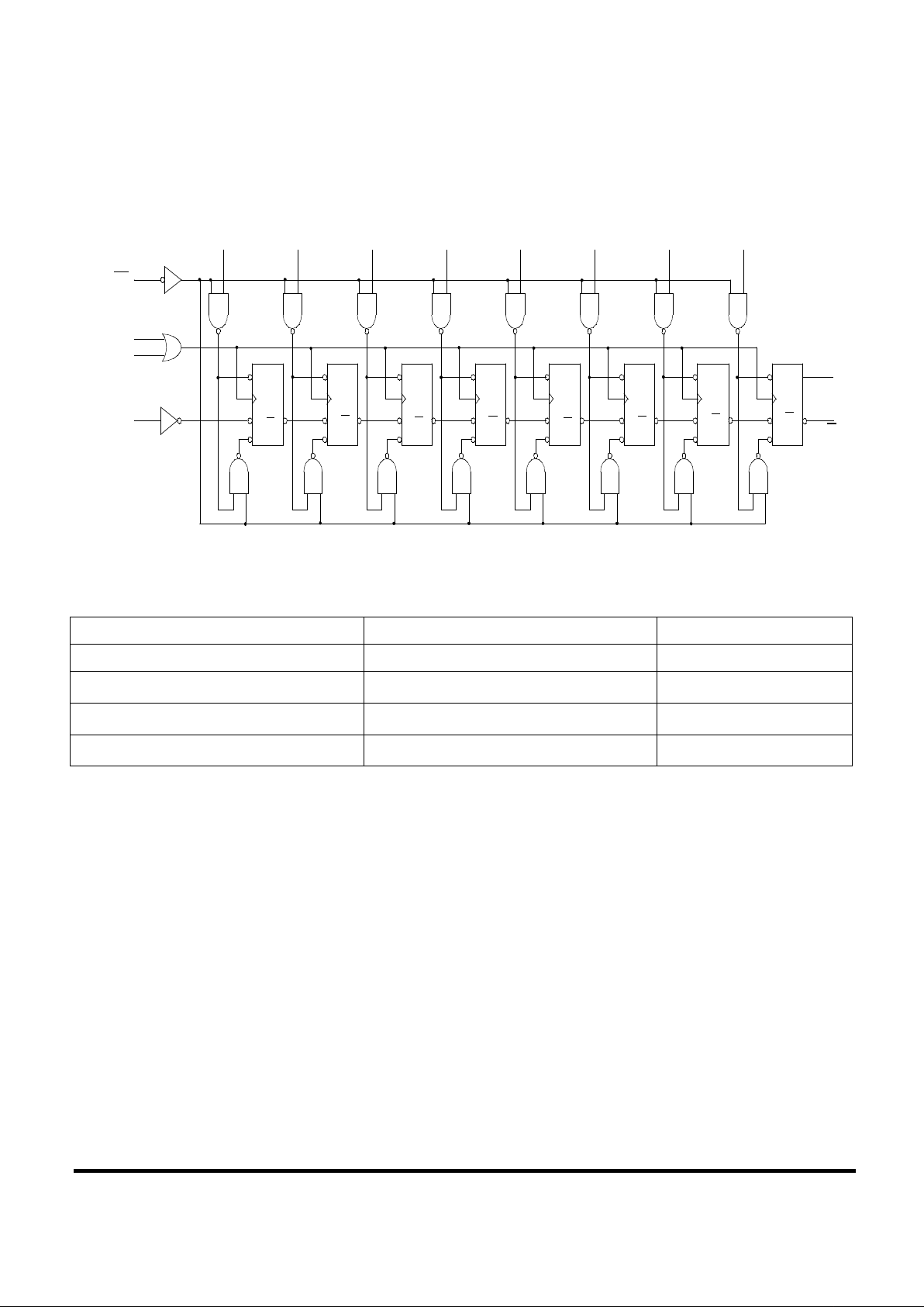
LOGIC DIAGRAM
RADIATION HARDNESS SPECIFICATIONS
1
Notes:
1. Logic will not latchup during radiation exposure within the limits defined in the table.
2. Device storage elements are immune to SEU affects.
PARAMETER LIMIT UNITS
Total Dose 1.0E6 rads(Si)
SEU Threshold
2
80
MeV-cm2/mg
SEL Threshold 120
MeV-cm2/mg
Neutron Fluence 1.0E14
n/cm
2
A B C D E F G
H
(11) (12) (13) (14) (4) (5) (6)
(3)
S
C
D
R
(1)
(15)
(2)
(10)
CLK INH
CLK
SER
Q
C
Q
D
Q
E
Q
F
Q
G
SH/LD
(9)
(7)
Q
H
Q
H
S
C
D
R
S
C
D
R
S
C
D
R
S
C
D
R
S
C
D
R
S
C
D
R
Q
A
S
C
D
R
Q
H
Q
B
Page 3

115 RadHard MSI Logic
UT54ACS165/UT54ACTS165
ABSOLUTE MAXIMUM RATINGS
Note:
1. Stresses outside the listed absolute maximum ratings may cause permanent damage to the device. This is a stress rating only, functional operation of the device
at these or any other conditions beyond limits indicated in the operational sections is not recommended. Exposure to absolute maximum rating conditions for
extended periods may affect device reliability.
RECOMMENDED OPERATING CONDITIONS
SYMBOL PARAMETER LIMIT UNITS
V
DD
Supply voltage -0.3 to 7.0 V
V
I/O
Voltage any pin -.3 to VDD +.3 V
T
STG
Storage Temperature range -65 to +150 C
T
J
Maximum junction temperature +175 C
T
LS
Lead temperature (soldering 5 seconds) +300 C
JC
Thermal resistance junction to case 20 C/W
I
I
DC input current 10 mA
P
D
Maximum power dissipation 1 W
SYMBOL PARAMETER LIMIT UNITS
V
DD
Supply voltage 4.5 to 5.5 V
V
IN
Input voltage any pin 0 to V
DD
V
T
C
Temperature range -55 to + 125 C
Page 4

RadHard MSI Logic 116
UT54ACS165/UT54ACTS165
DC ELECTRICAL CHARACTERISTICS
7
(VDD = 5.0V 10%; VSS = 0V 6, -55 C < TC < +125 C)
SYMBOL PARAMETER CONDITION MIN MAX UNIT
V
IL
Low-level input voltage
1
ACTS
ACS
0.8
.3V
DD
V
V
IH
High-level input voltage
1
ACTS
ACS
.5V
DD
.7V
DD
V
I
IN
Input leakage current
ACTS/ACS VIN = V
DD
or V
SS
-1
1 A
V
OL
Low-level output voltage
3
ACTS
ACS
I
OL
= 8.0mA
I
OL
= 100 A
0.40
0.25
V
V
OH
High-level output voltage
3
ACTS
ACS
I
OH
= -8.0mA
I
OH
= -100 A
.7V
DD
VDD - 0.25
V
I
OS
Short-circuit output current
2 ,4
ACTS/ACS
VO = VDD and V
SS
-200 200 mA
I
OL Output current
10
(Sink)
VIN = VDD or V
SS
VOL = 0.4V
8 mA
I
OH
Output current
10
(Source)
VIN = VDD or V
SS
VOH = VDD - 0.4V
-8 mA
P
total
Power dissipation
2, 8, 9
CL = 50pF 2.9 mW/MHz
I
DDQ
Quiescent Supply Current VDD = 5.5V 10 A
I
DDQ
Quiescent Supply Current Delta
ACTS
For input under test
VIN = VDD - 2.1V
For all other inputs
VIN = VDD or V
SS
V
DD
= 5.5V
1.6 mA
C
IN Input capacitance
5
= 1MHz @ 0V 15 pF
C
OUT Output capacitance
5
= 1MHz @ 0V 15 pF
Page 5

117 RadHard MSI Logic
UT54ACS165/UT54ACTS165
Notes:
1. Functional tests are conducted in accordance with MIL-STD-883 with the following input test conditions: VIH = VIH(min) + 20%, - 0%; VIL = VIL(max) + 0%,
- 50%, as specified herein, for TTL, CMOS, or Schmitt compatible inputs. Devices may be tested using any input voltage within the above specified range, but
are guaranteed to VIH(min) and VIL(max).
2. Supplied as a design limit but not guaranteed or tested.
3. Per MIL-PRF-38535, for current density 5.0E5 amps/cm2, the maximum product of load capacitance (per output buffer) times frequency should not exceed
3,765 pF/MHz.
4. Not more than one output may be shorted at a time for maximum duration of one second.
5. Capacitance measured for initial qualification and when design changes may affect the value. Capacitance is measured between the designated terminal and VSS
at frequency of 1MHz and a signal amplitude of 50mV rms maximum.
6. Maximum allowable relative shift equals 50mV.
7. All specifications valid for radiation dose 1E6 rads(Si).
8. Power does not include power contribution of any TTL output sink current.
9. Power dissipation specified per switching output.
10. This value is guaranteed based on characterization data, but not tested.
Page 6

RadHard MSI Logic 118
UT54ACS165/UT54ACTS165
AC ELECTRICAL CHARACTERISTICS
2
(VDD = 5.0V 10%; VSS = 0V 1, -55 C < TC < +125 C)
Notes:
1. Maximum allowable relative shift equals 50mV.
2. All specifications valid for radiation dose 1E6 rads(Si).
3. Based on characterization, hold time (tH3) of 0ns for data pins A-H, can be assumed if data setup time (t
SU2
) is >10ns. This is guaranteed, but not tested.
SYMBOL PARAMETER MINIMUM MAXIMUM UNIT
t
PHL
CLK or CLK INH to Q
H
or Q
H
2 21 ns
t
PLH
CLK or CLK INH to QH or Q
H
2 18 ns
t
PHL
SH/LD to QH or Q
H
2 21 ns
t
PLH
SH/LD to QH or Q
H
2 18 ns
t
PHL
H to Q
H
2 21 ns
t
PLH
H to Q
H
2 17 ns
t
PHL
H to Q
H
2 20 ns
t
PLH
H to Q
H
2 18 ns
f
MAX
Maximum clock frequency 71 MHz
t
SU1
SER, SH/LD, CLKINH or CLK
Setup time before CLK or CLK INH
7 ns
t
SU2
Data setup time before SH/LD 7 ns
t
H1
SER hold time after CLK or CLK INH 2 ns
t
H2
CLK INH hold time after CLK 2 ns
t
H3
3
Hold time for any input after SH/LD 2 ns
t
W
Minimum pulse width
CLK or CLK INH high
CLK or CLK INH low
SH/LD
7 ns
 Loading...