

Page 1
101 RadHard MSI Logic
UT54ACS163/UT54ACTS163
Radiation-Hardened
4-Bit Synchronous Counters
FEATURES
Internal look-ahead for fast counting
Carry output for n-bit cascading
Synchronous counting
Synchronously programmable
radiation-hardened CMOS
- Latchup immune
High speed
Low power consumption
Single 5 volt supply
Available QML Q or V processes
Flexible package
- 16-pin DIP
- 16-lead flatpack
DESCRIPTION
The UT54ACS163 and the UT54ACTS163 are synchronous
presettable 4-bit binary counters that feature internal carry lookahead logic for high-speed counting designs. Synchronous operation occurs by having all flip-flops clocked simultaneously
so that the outputs change coincident with each other when instructed by the count-enable inputs and internal gating. A buffered clock input triggers the four flip-flops on the rising (positive-going) edge of the clock input waveform.
The counters are fully programmable (i.e., they may be preset
to any number between 0 and 15). Presetting is synchronous;
applying a low level at the load input disables the counter and
causes the outputs to agree with the load data after the next clock
pulse.
The clear function is synchronous and a low level at the clear
input sets all four of the flip-flop outputs low after the next clock
pulse. This synchronous clear allows the count length to be modified by decoding the Q outputs for the maximum count desired.
The counters feature a fully independent clock circuit. Changes
at control inputs (ENP, ENT, or LOAD) that modify the operating mode have no effect on the contents of the counter until
clocking occurs. The function of the counter (whether enabled,
disabled, loading, or counting) will be dictated solely by the
conditions meeting the stable setup and hold times.
The devices are characterized over full military temperature
range of -55 C to +125 C.
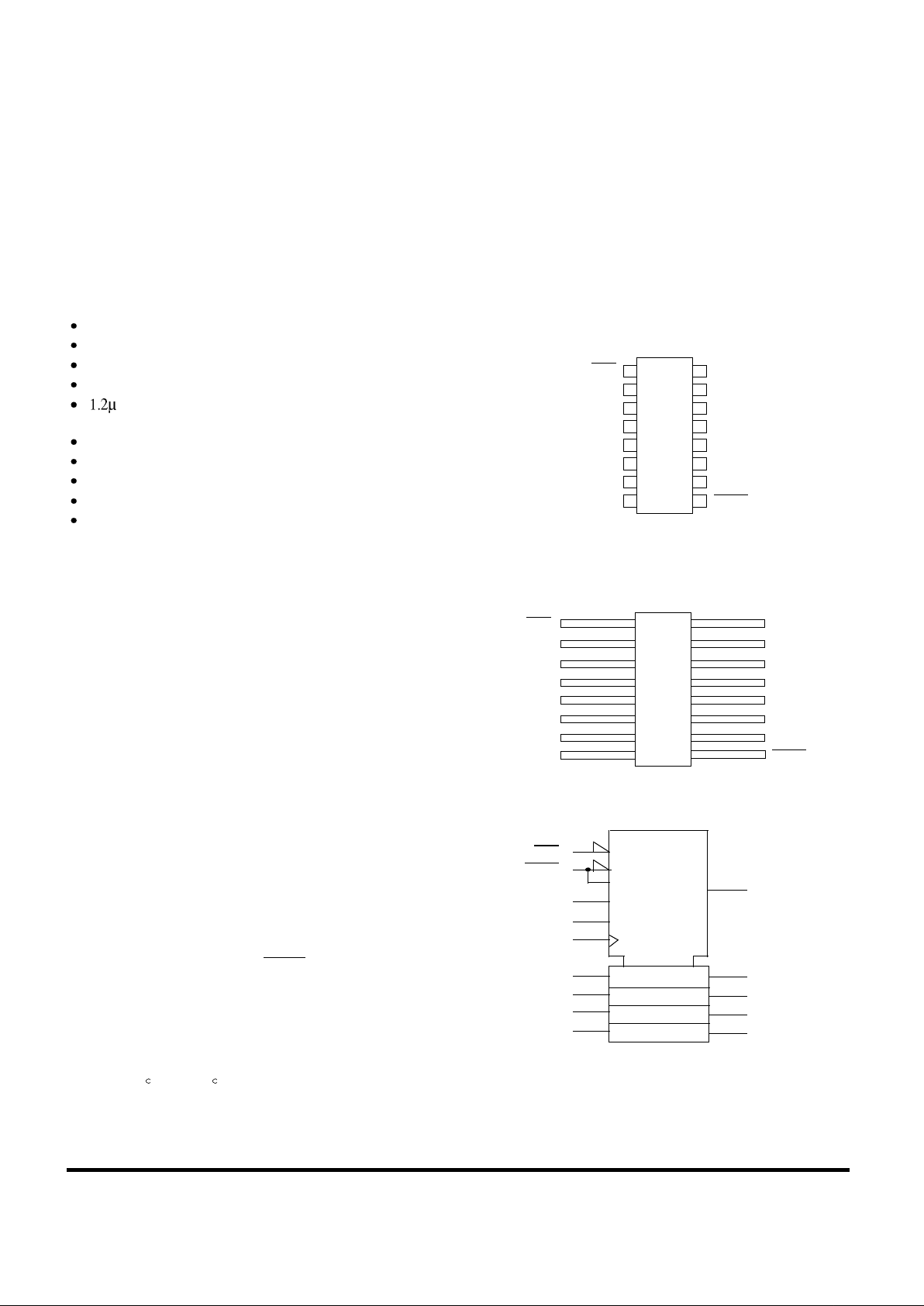
PINOUTS
16-Pin DIP
Top View
16-Lead Flatpack
Top View
LOGIC SYMBOL
1
2
3
4
5
7
6
16
15
14
13
12
10
11
CLR
CLK
A
B
C
D
ENP
V
DD
RCO
Q
A
Q
B
Q
C
Q
D
ENT
8 9V
SS
LOAD
1
2
3
4
5
7
6
16
15
14
13
12
10
11
V
DD
8 9
CLR
CLK
A
B
C
D
ENP
RCO
Q
A
Q
B
Q
C
Q
D
ENT
V
SS
LOAD
(1)
CLR
(9)
LOAD M1
5CT=0
CTRDIV 16
(10)
ENT
G3
(7)
ENP G4
(2)
CLK
(3)
A
(4)
B
(5)
C
(6)
D
(15)
RCO
(14)
Q
A
(11)
Q
D
M2
C5/2,3,4+
(12)
Q
C
(13)
Q
B
1,5D
(1)
(2)
(4)
(8)
3CT = 15
Note:
1. Logic symbol in accordance with ANSI/IEEE Std 91-1984 and IEC Publication 617-12.
Page 2
RadHard MSI Logic 102
UT54ACS163/UT54ACTS163
FUNCTION TABLE
H = High voltage level h = High voltage level one setup time prior to the low-to-high clock transition
L = Low voltage level l = Low voltage level one setup time prior to the low-to-high clock transition
Notes:
1. The RCO output is high when ENT is high and the counter is at terminal count HHHH.
2. The high-to-low transition of ENP or ENT should only occur while CLK is high for conventional operations.
3. The low-to-high transition of LOAD or CLR should only occur while CLK is high for conventional operations.
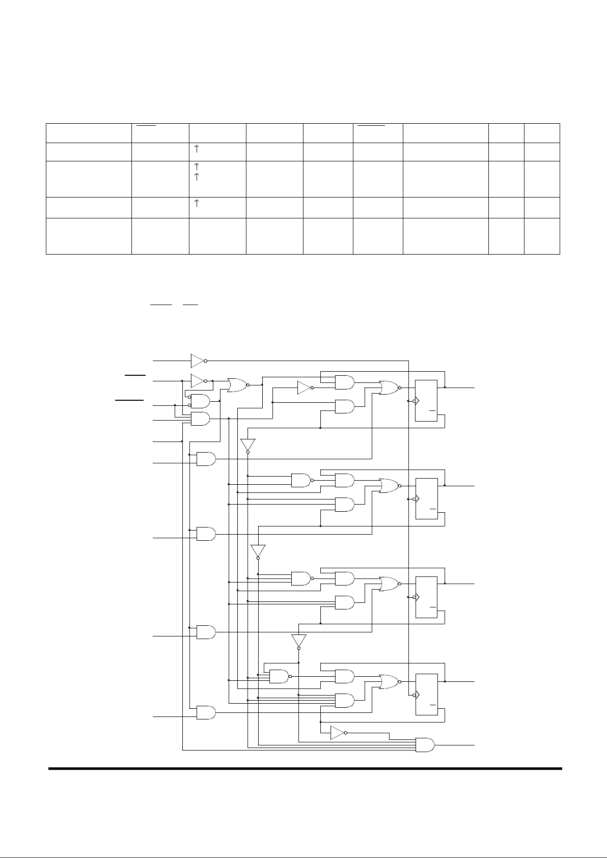
LOGIC DIAGRAM
Operating Mode CLR CLK ENP ENT LOAD DATA A,B,C,D Q
N
RCO
Reset (Clear) l X X X X L L
Parallel Load
h
3
h
3
X
X
X
X
l
l
l
h
L
H
L
1
Count
h
3
h h h X Count
1
Inhibit
h
3
h
3
X
X
l 2
X
X
l
2
h
3
h
3
X
X
Q
N
Q
N
1
L
(2)
(1)
(9)
(7)
(10)
(3)
(4)
(5)
(6)
(14)
(12)
(13)
(11)
(15)
Q
A
Q
B
Q
C
Q
D
RCO
DATA D
DATA C
DATA B
DATA A
ENT
ENP
LOAD
CLR
CLK
C
D
Q
Q
C
D
Q
Q
C
D
Q
Q
C
D
Q
Q
Page 3

103 RadHard MSI Logic
UT54ACS163/UT54ACTS163
RADIATION HARDNESS SPECIFICATIONS
1
Notes:
1. Logic will not latchup during radiation exposure within the limits defined in the table.
2. Device storage elements are immune to SEU affects.
ABSOLUTE MAXIMUM RATINGS
Note:
1. Stresses outside the listed absolute maximum ratings may cause permanent damage to the device. This is a stress rating only, functional operation of the
device at these or any other conditions beyond limits indicated in the operational sections is not recommended. Exposure to absolute maximum rating
conditions for extended periods may affect device reliability.
RECOMMENDED OPERATING CONDITIONS
PARAMETER LIMIT UNITS
Total Dose 1.0E6 rads(Si)
SEU Threshold
2
80
MeV-cm2/mg
SEL Threshold 120
MeV-cm2/mg
Neutron Fluence 1.0E14
n/cm
2
SYMBOL PARAMETER LIMIT UNITS
V
DD
Supply voltage 0.3 to 7.0 V
V
I/O
Voltage any pin -.3 to VDD +.3 V
T
STG
Storage Temperature range -65 to +150 C
T
J
Maximum junction temperature +175 C
T
LS
Lead temperature (soldering 5 seconds) +300 C
JC
Thermal resistance junction to case 20 C/W
I
I
DC input current 10 mA
P
D
Maximum power dissipation 1 W
SYMBOL PARAMETER LIMIT UNITS
V
DD
Supply voltage 4.5 to 5.5 V
V
IN
Input voltage any pin 0 to V
DD
V
T
C
Temperature range -55 to + 125 C
Page 4

RadHard MSI Logic 104
UT54ACS163/UT54ACTS163
DC ELECTRICAL CHARACTERISTICS
7
(VDD = 5.0V 10%; VSS = 0V 6, -55 C < TC < +125 C)
SYMBOL PARAMETER CONDITION MIN MAX UNIT
V
IL Low-level input voltage
1
ACTS
ACS
0.8
.3V
DD
V
V
IH High-level input voltage
1
ACTS
ACS
.5V
DD
.7V
DD
V
I
IN
Input leakage current
ACTS/ACS VIN = V
DD
or V
SS
-1
1 A
V
OL Low-level output voltage
3
ACTS
ACS
I
OL
= 8.0mA
I
OL
= 100 A
0.40
0.25
V
V
OH High-level output voltage
3
ACTS
ACS
I
OH
= -8.0mA
I
OH
= -100 A
.7V
DD
VDD - 0.25
V
I
OS
Short-circuit output current
2 ,4
ACTS/ACS
VO = VDD and V
SS
-200 200 mA
I
OL
Output current
10
(Sink)
VIN = VDD or V
SS
VOL = 0.4V
8 mA
I
OH
Output current
10
(Source)
VIN = VDD or V
SS
VOH = VDD - 0.4V
-8 mA
P
total
Power dissipation
2, 8, 9
CL = 50pF 1.9 mW/MHz
I
DDQ
Quiescent Supply Current VDD = 5.5V 10 A
I
DDQ
Quiescent Supply Current Delta
ACTS
For input under test
VIN = VDD - 2.1V
For all other inputs
VIN = VDD or V
SS
V
DD
= 5.5V
1.6 mA
C
IN
Input capacitance
5
= 1MHz @ 0V 15 pF
C
OUT
Output capacitance 5
= 1MHz @ 0V 15 pF
Page 5

105 RadHard MSI Logic
UT54ACS163/UT54ACTS163
Notes:
1. Functional tests are conducted in accordance with MIL-STD-883 with the following input test conditions: VIH = VIH(min) + 20%, - 0%; VIL = VIL(max) + 0%,
- 50%, as specified herein, for TTL, CMOS, or Schmitt compatible inputs. Devices may be tested using any input voltage within the above specified range, but
are guaranteed to VIH(min) and VIL(max).
2. Supplied as a design limit but not guaranteed or tested.
3. Per MIL-PRF-38535, for current density 5.0E5 amps/cm2, the maximum product of load capacitance (per output buffer) times frequency should not exceed
3,765 pF/MHz.
4. Not more than one output may be shorted at a time for maximum duration of one second.
5. Capacitance measured for initial qualification and when design changes may affect the value. Capacitance is measured between the designated terminal and VSS
at frequency of 1MHz and a signal amplitude of 50mV rms maximum.
6. Maximum allowable relative shift equals 50mV.
7. All specifications valid for radiation dose 1E6 rads(Si).
8. Power does not include power contribution of any TTL output sink current.
9. Power dissipation specified per switching output.
10. This value is guaranteed based on characterization data, but not tested.
Page 6

RadHard MSI Logic 106
UT54ACS163/UT54ACTS163
AC ELECTRICAL CHARACTERISTICS
2
(VDD = 5.0V 10%; VSS = 0V 1, -55 C < TC < +125 C)
Notes:
1. Maximum allowable relative shift equals 50mV.
2. All specifications valid for radiation dose 1E6 rads(Si).
3. Based on characterization, hold time (tH1) of 0ns can be assumed if data setup time (t
SU1
) is >10ns. This is guaranteed, but not tested.
SYMBOL PARAMETER MINIMUM MAXIMUM UNIT
t
PHL
CLK to Q
n
4 24 ns
t
PLH
CLK to Qn 4 22 ns
t
PHL
CLK to RCO 4 22 ns
t
PLH
CLK to RCO 4 24 ns
t
PHL
ENT to RCO 1 13 ns
t
PLH
ENT to RCO 1 14 ns
f
MAX
Maximum clock frequency 77 MHz
t
SU1
A, B, C, D
Setup time before CLK
6 ns
t
SU2
LOAD, ENP, ENT, CLR low or high
Setup time before CLK
6 ns
t
H1
3
Data hold time after CLK 1 ns
t
H2
All synchronous inputs hold time after CLK 1 ns
t
W
Minimum pulse width
CLR low
CLK high
CLK low
7 ns
 Loading...