

Page 1
UT54ACS132/UT54ACTS132
Radiation-Hardened
Quadruple 2-Input NAND Schmitt Triggers
FEATURES
• radiation-hardened CMOS
- Latchup immune
• High speed
• Low power consumption
• Single 5 volt supply
• Available QML Q or V processes
• Flexible package
- 14-pin DIP
- 14-lead flatpack
DESCRIPTION
The UT54ACS132 and the UT54ACTS132 are 2-input NAND
gates with Schmitt Trigger input levels. A high applied on both
the inputs forces the output to a low state.
The devices are characterized over full military temperature
range of -55 C to +125 C.
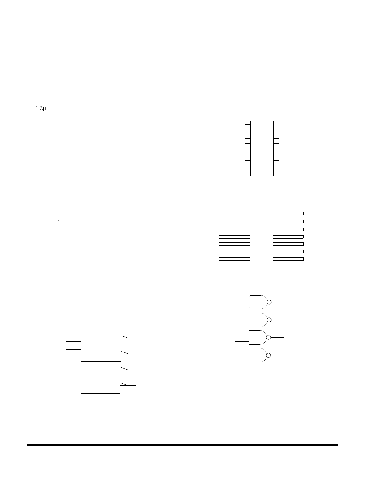
FUNCTION TABLE
INPUTS OUTPUT
An Bn Yn
L L H
L H H
H L H
H H L
LOGIC SYMBOL
(1)
A1
B1
A2
B2
A3
B3
A4
B4
(2)
(4)
(5)
(9)
(10)
(12)
(13)
&
(3)
(6)
(8)
(11)
Y1
Y2
Y3
Y4
PINOUTS
A1
B1
Y1
A2
B2
Y2
V
A1
B1
Y1
A2
B2
Y2
V
SS
LOGIC DIAGRAM
A1
B1
A2
B2
A3
B3
A4
B4
14-Pin DIP
Top View
1 14
2 13
3 12
4 11
5 10
6 9
7 8
SS
14-Lead Flatpack
Top View
1 14
2 13
3 12
4 11
5 10
6 9
7 8
V
B4
A4
Y4
B3
A3
Y3
DD
Y1
Y2
Y3
Y4
V
B4
A4
Y4
B3
A3
Y3
DD
Note:
1. Logic symbol in accordance with ANSI/IEEE standard 91-1984
and IEC Publication 617-12.
67 RadHard MSI Logic
Page 2
UT54ACS132/UT54ACTS132
RADIATION HARDNESS SPECIFICATIONS
1
PARAMETER LIMIT UNITS
Total Dose 1.0E6 rads(Si)
SEU Threshold
2
80
SEL Threshold 120
Neutron Fluence 1.0E14
Notes:
1. Logic will not latchup during radiation exposure within the limits defined in the table.
2. Device storage elements are immune to SEU affects.
ABSOLUTE MAXIMUM RATINGS
SYMBOL PARAMETER LIMIT UNITS
T
V
V
T
DD
I/O
STG
T
J
LS
Maximum junction temperature +175 C
Lead temperature (soldering 5 seconds) +300 C
Supply voltage -0.3 to 7.0 V
Voltage any pin -.3 to VDD +.3 V
Storage Temperature range -65 to +150 C
MeV-cm2/mg
MeV-cm2/mg
2
n/cm
JC
I
I
P
D
Note:
1. Stresses outside the listed absolute maximum ratings may cause permanent damage to the device. This is a stress rating only, functional operation of the device
at these or any other conditions beyond limits indicated in the operational sections is not recommended. Exposure to absolute maximum rating conditions for
extended periods may affect device reliability.
Thermal resistance junction to case 20 C/W
DC input current 10 mA
Maximum power dissipation 1 W
RECOMMENDED OPERATING CONDITIONS
SYMBOL PARAMETER LIMIT UNITS
V
DD
V
IN
T
C
Supply voltage 4.5 to 5.5 V
Input voltage any pin 0 to V
DD
Temperature range -55 to + 125 C
V
RadHard MSI Logic 68
Page 3

UT54ACS132/UT54ACTS132
DC ELECTRICAL CHARACTERISTICS
7
(VDD = 5.0V 10%; VSS = 0V 6, -55 C < TC < +125 C)
SYMBOL PARAMETER CONDITION MIN MAX UNIT
VT+
VT-
V
I
IN
V
OL
V
OH
H
Schmitt Trigger, positive going 1 threshold
ACTS
ACS
Schmitt Trigger, negative going 1 threshold
ACTS
ACS
Schmitt Trigger, typical range of hysteresis
2
ACTS
ACS
Input leakage current
ACTS/ACS VIN = V
Low-level output voltage
3
ACTS
ACS
High-level output voltage
ACTS
ACS
3
I
I
I
= 8.0mA
OL
I
= 100 A
OL
= -8.0mA
OH
= -100 A
OH
DD
or V
SS
2.25
.7V
DD
0.5
.3V
DD
0.3
0.6
0.9
1.5
-1 1 A
0.40
0.25
.7V
DD
VDD - 0.25
V
V
V
V
V
I
OS
Short-circuit output current
ACTS/ACS
I
OL
Output current
(Sink)
I
OH Output current
(Source)
P
total
I
DDQ
I
DDQ
Power dissipation
Quiescent Supply Current VDD = 5.5V 10 A
Quiescent Supply Current Delta
ACTS
C
C
IN
OUT
Input capacitance
Output capacitance 5
2 ,4
10
VO = VDD and V
VIN = VDD or V
SS
SS
-200 200 mA
8 mA
VOL = 0.4V
10
VIN = VDD or V
SS
-8 mA
VOH = VDD - 0.4V
2, 8, 9
CL = 50pF 1.9 mW/
MHz
For input under test
3.1 mA
VIN = VDD - 2.1V
For all other inputs
VIN = VDD or V
V
= 5.5V
DD
5
= 1MHz @ 0V 15 pF
SS
= 1MHz @ 0V 15 pF
69 RadHard MSI Logic
Page 4

UT54ACS132/UT54ACTS132
Notes:
1. Functional tests are conducted in accordance with MIL-STD-883 with the following input test conditions: VIH = VIH(min) + 20%, - 0%; VIL = VIL(max) + 0%,
- 50%, as specified herein, for TTL, CMOS, or Schmitt compatible inputs. Devices may be tested using any input voltage within the above specified range, but
are guaranteed to VIH(min) and VIL(max).
2. Supplied as a design limit but not guaranteed or tested.
3. Per MIL-PRF-38535, for current density 5.0E5 amps/cm2, the maximum product of load capacitance (per output buffer) times frequency should not exceed
3,765 pF/MHz.
4. Not more than one output may be shorted at a time for maximum duration of one second.
5. Capacitance measured for initial qualification and when design changes may affect the value. Capacitance is measured between the designated terminal and VSS
at frequency of 1MHz and a signal amplitude of 50mV rms maximum.
6. Maximum allowable relative shift equals 50mV.
7. All specifications valid for radiation dose 1E6 rads(Si).
8. Power does not include power contribution of any TTL output sink current.
9. Power dissipation specified per switching output.
10. This value is guaranteed based on characterization data, but not tested.
AC ELECTRICAL CHARACTERISTICS
(VDD = 5.0V 10%; VSS = 0V 1, -55 C < TC < +125 C)
2
SYMBOL PARAMETER MINIMUM MAXIMUM UNIT
t
PHL
t
PLH
Notes:
1. Maximum allowable relative shift equals 50mV.
2. All specifications valid for radiation dose 1E6 rads(Si).
Input to Yn 2 15 ns
Input to Yn 2 12 ns
RadHard MSI Logic 70
 Loading...