

Page 1
RTMP-1
UT1553 Remote Terminal Multi-Protocol
FEATURES
p Complete MIL-STD-1553 Remote Terminal Interface
p Mode selectable to comply with either MIL-STD-
1553A or MIL-STD-1553B bus protocol
p Mil-STD-1773 compatible
p Remote terminal operation is certified by ASD/
ENASC (SEAFAC)
p Implements all dual-redundant Remote Terminal mode
codes and operational functions including broadcast
commands
p Provides handshake control for quad-redundant
systems
p Data pointers permit programmable memory mapping
for 1553 data over the entire 64K host memory space
p Provides all handshaking signals for a DMA interface
p Stores 1553 command word and time-tag information
with all incoming data for enhanced data management
p Three-state address bus, databus, and control signals
simplify DMA operations
p Supports end-of-command activity and data bus error
interrupts
p Self-test capability
p Available as a gate array macrocell
p Available in 84-pin pingrid array, 84-lead leadless chip
carrier, or 84-lead flatpack packages
p Standard Microcircuit Drawing 5962-88645 available
- QML Q compliant
INTRODUCTION
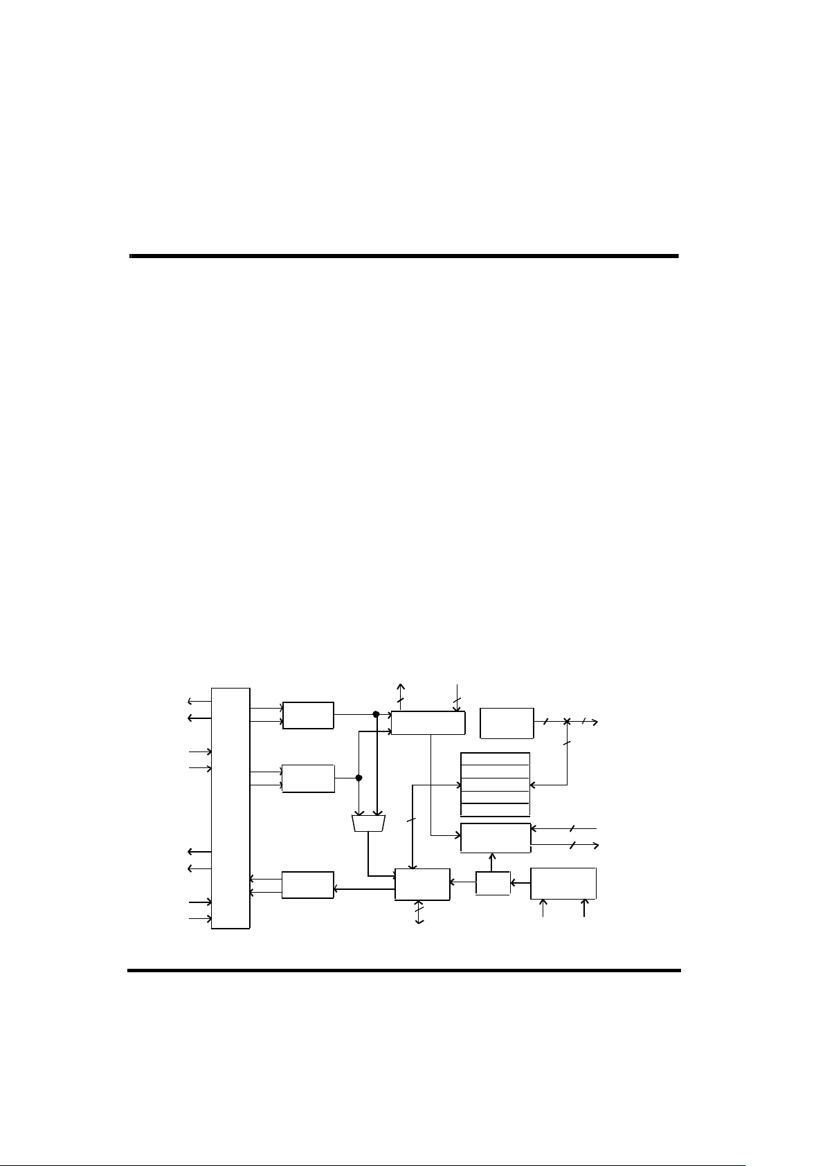
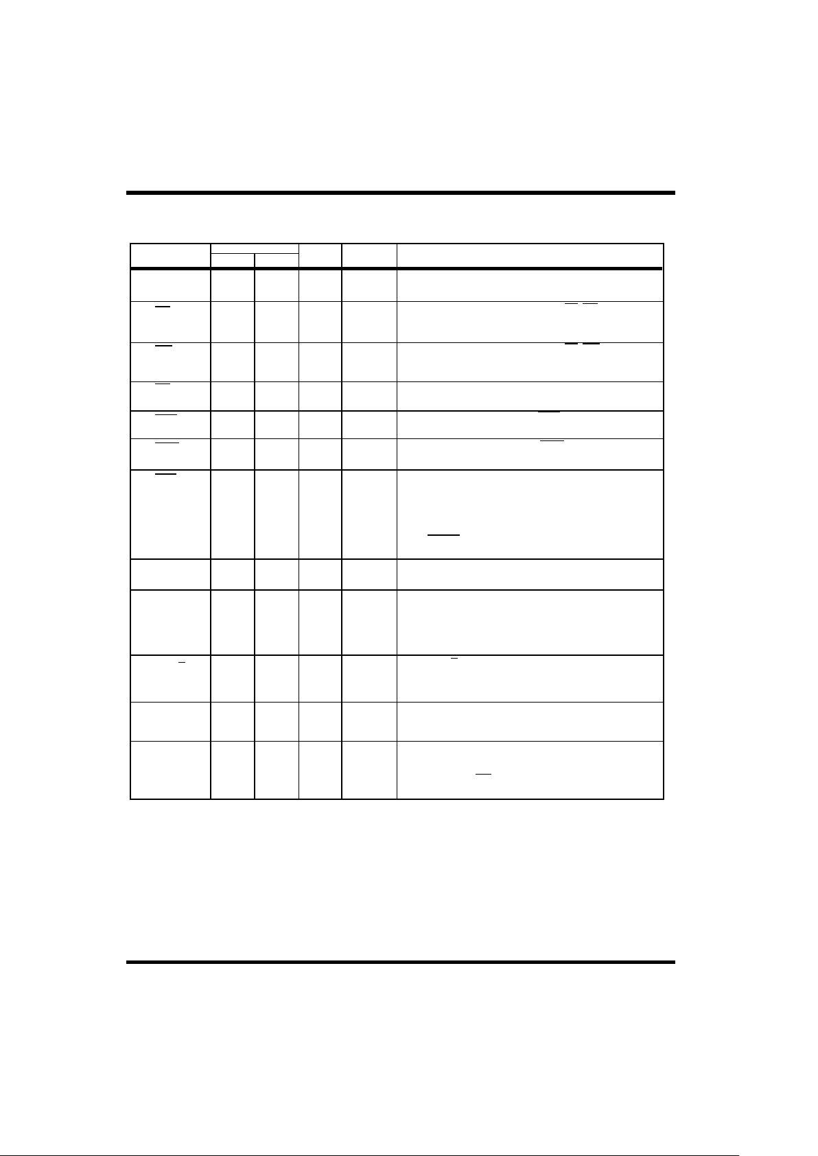
The UT1553 RTMP (figures 1 and 4) is a monolithic,
CMOS, VLSI integrated circuit that meets all requirements
for a dual-redundant MIL-STD-1553 Remote Terminal
interface. The RTMP’s advanced design supports both
MIL-STD-1553A and MIL-STD-1553B serial data bus
protocols, including differences in the status word response
time and bit definitions, providing the system designer a
single-chip solution to most Remote Terminal interface
requirements.
The UT1553 RTMP provides all requisite 1553 protocol and
data handling, 1553 message error checking, DMA
handshake and control signals, and comprehensive self-test
capabilities. The RTMP’s pointer-based, programmable
memory-mapping architecture permits the host to map 1553
message data anywhere in the 64K memory space. This
advanced memory mapping, along with the RTMP’s control
and status functions, minimize the host system’s 1553
interface overhead.
The UT1553 RTMP is a member of UTMC’s complete
family of high-reliability monolithic MIL-STD-1553
interface products.
16
55
SUBADDRESS ADDRESS
TERMINALMODE CODE/
3
16
16
16
9
13
OUTPUTS
CONTROL
INPUTS
CONTROL
ADDRESS
MEMORY
CONTROL
ADDRESS
MEMORY
DATA
TIME TAG
CONTROL
BASE PTR
STATUS
LAST CMD
LOGIC
CONTROL
AND ERROR
12MHz
RESET
MASTER
LOGIC
RESET
CLOCK AND
TIMER
LOGIC
TRANSFER
LOGIC
DATA
COMMAND
RECOGNITION
MUX
OUT
IN
A
OUT
IN
B
DECODER
DECODER
ENCODER
CHANNEL
CHANNEL
OUTPUT MULTIPLEXING AND
SELF-TEST WRAPAROUNDLOGIC
Figure 1. UT1553 RTMP Functional Block Diagram
Page 2

RTMP-2
Table of Contents
1.0 FUNCTIONAL DESCRIPTION . . . . . . . . . . . . . . . . . . . . . . . . . . . . . . . . . . . . . . . .3
2.0 PIN IDENTIFICATION AND DESCRIPTION. . . . . . . . . . . . . . . . . . . . . . . . . . . .5
3.0 REMOTE TERMINAL ARCHITECTURE. . . . . . . . . . . . . . . . . . . . . . . . . . . . . .11
3.1 Internal Registers . . . . . . . . . . . . . . . . . . . . . . . . . . . . . . . . . . . . . . . . . . . . . . .11
3.2 Read/Write Register . . . . . . . . . . . . . . . . . . . . . . . . . . . . . . . . . . . . . . . . . . . . .11
3.3 Time Tag Data Register . . . . . . . . . . . . . . . . . . . . . . . . . . . . . . . . . . . . . . . . . .11
3.4 Control Register . . . . . . . . . . . . . . . . . . . . . . . . . . . . . . . . . . . . . . . . . . . . . . . .13
3.5 Base Pointer Data Register . . . . . . . . . . . . . . . . . . . . . . . . . . . . . . . . . . . . . . . .15
3.6 Read Only Registers . . . . . . . . . . . . . . . . . . . . . . . . . . . . . . . . . . . . . . . . . . . . .15
3.6.1 Operational Status Register. . . . . . . . . . . . . . . . . . . . . . . . . . . . . . . . . .16
3.6.2 Last 1553 Command Register. . . . . . . . . . . . . . . . . . . . . . . . . . . . . . . .17
3.7 Write Only Register . . . . . . . . . . . . . . . . . . . . . . . . . . . . . . . . . . . . . . . . . . . . .17
4.0 REMOTE TERMINAL INTERFACE OPERATION. . . . . . . . . . . . . . . . . . . . . .17
4.1 Programming the BPD . . . . . . . . . . . . . . . . . . . . . . . . . . . . . . . . . . . . . . . . . . .17
4.2 RTMP Pointer Block. . . . . . . . . . . . . . . . . . . . . . . . . . . . . . . . . . . . . . . . . . . . .17
4.3 Pointer Block Location Definition . . . . . . . . . . . . . . . . . . . . . . . . . . . . . . . . . .19
4.4 RTMP Data Storage . . . . . . . . . . . . . . . . . . . . . . . . . . . . . . . . . . . . . . . . . . . . .21
4.5 RTMP Interrupt Function . . . . . . . . . . . . . . . . . . . . . . . . . . . . . . . . . . . . . . . . .21
4.6 RTMP Error Detection Capabilities . . . . . . . . . . . . . . . . . . . . . . . . . . . . . . . . .22
4.6.1 Terminal Address Parity Errors . . . . . . . . . . . . . . . . . . . . . . . . . . . . . . .22
4.6.2 Framing or Overrun Error. . . . . . . . . . . . . . . . . . . . . . . . . . . . . . . . . . . .23
4.6.3 1553 Message Errors . . . . . . . . . . . . . . . . . . . . . . . . . . . . . . . . . . . . . . .24
4.7 RTMP Self-Test Function. . . . . . . . . . . . . . . . . . . . . . . . . . . . . . . . . . . . . . . . .24
5.0 1553A AND 1553B MODES OF OPERATION . . . . . . . . . . . . . . . . . . . . . . . . . . .25
5.1 Status Word Bit Definition . . . . . . . . . . . . . . . . . . . . . . . . . . . . . . . . . . . . . . . .26
5.2 Mode Code Responses . . . . . . . . . . . . . . . . . . . . . . . . . . . . . . . . . . . . . . . . . . .26
5.3 Status Word Response Time . . . . . . . . . . . . . . . . . . . . . . . . . . . . . . . . . . . . . . .26
6.0 RTMP SYSTEM INTERFACE . . . . . . . . . . . . . . . . . . . . . . . . . . . . . . . . . . . . . . . .27
6.1Assigning the Terminal. . . . . . . . . . . . . . . . . . . . . . . . . . . . . . . . . . . . . . . . . . . . . .28
6.2Controlling the DMA Interface. . . . . . . . . . . . . . . . . . . . . . . . . . . . . . . . . . . . . . . .28
6.3Interfacing with the RTMP’s Internal Register . . . . . . . . . . . . . . . . . . . . . . . . . . .29
6.4RTMP Hardware Interface . . . . . . . . . . . . . . . . . . . . . . . . . . . . . . . . . . . . . . . . . . .29
6.4.1 RTMP -- 1553 Transceiver Interface. . . . . . . . . . . . . . . . . . . . . . . . . . . .29
6.4.2 RTMP DMA Interface. . . . . . . . . . . . . . . . . . . . . . . . . . . . . . . . . .29
7.0 MAXIMUM AND RECOMMENDED OPERATING CONDITIONS31
8.0 DC ELECTRICAL CHARACTERISTICS . . . . . . . . . . . . . . . . . . . . . . . . . . . . . . .3
9.0 AC ELECTRICAL CHARACTERISTICS . . . . . . . . . . . . . . . . . . . . . . . . . . . . . .33
10.0 PACKAGE OUTLINE DRAWINGS. . . . . . . . . . . . . . . . . . . . . . . . . . . . . . . . . . . .39
Page 3

RTMP-3
FUNCTIONAL DESCRIPTION
General Description
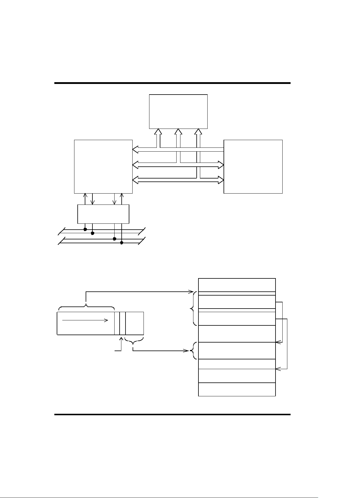
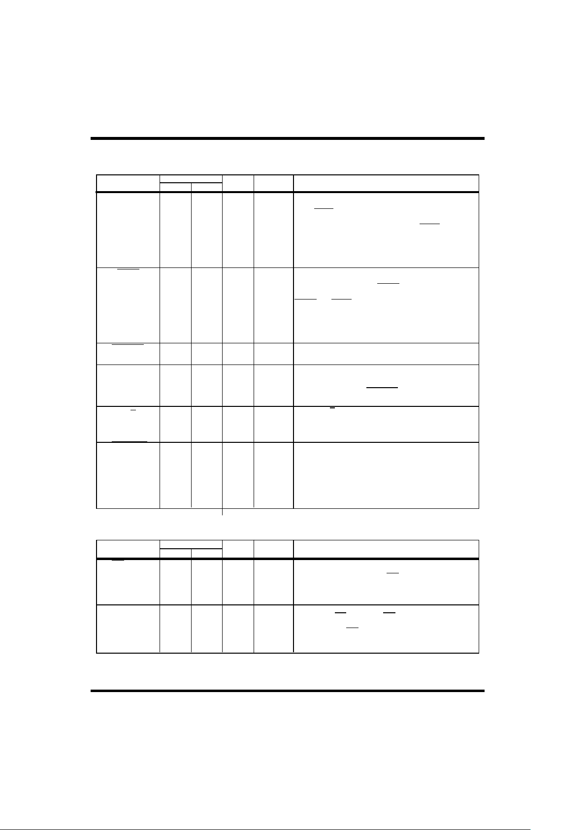
The RTMP is an interface device linking a MIL-STD-1553
serial data bus and a host microprocessor system (figure 2).
By selecting the correct state of the 1553 protocol select pin
(PRA/B = 1 for 1553A, 0 for 1553B), the system designer
can program the RTMP to comply fully with either MILSTD-1553A or MIL-STD-1553B.
The link between the 1553 data bus and the RTMP is the
shared memory area. All the data the RTMP transmits or
receives over the 1553 bus is stored in this shared memory
area. The RTMP accesses the shared memory with its DMA
signals (DMAR, DMAG, and DMAEN), the 16-bit
bidirectional data bus (D0-D15), and the 16-bit address bus
(A0-A15).
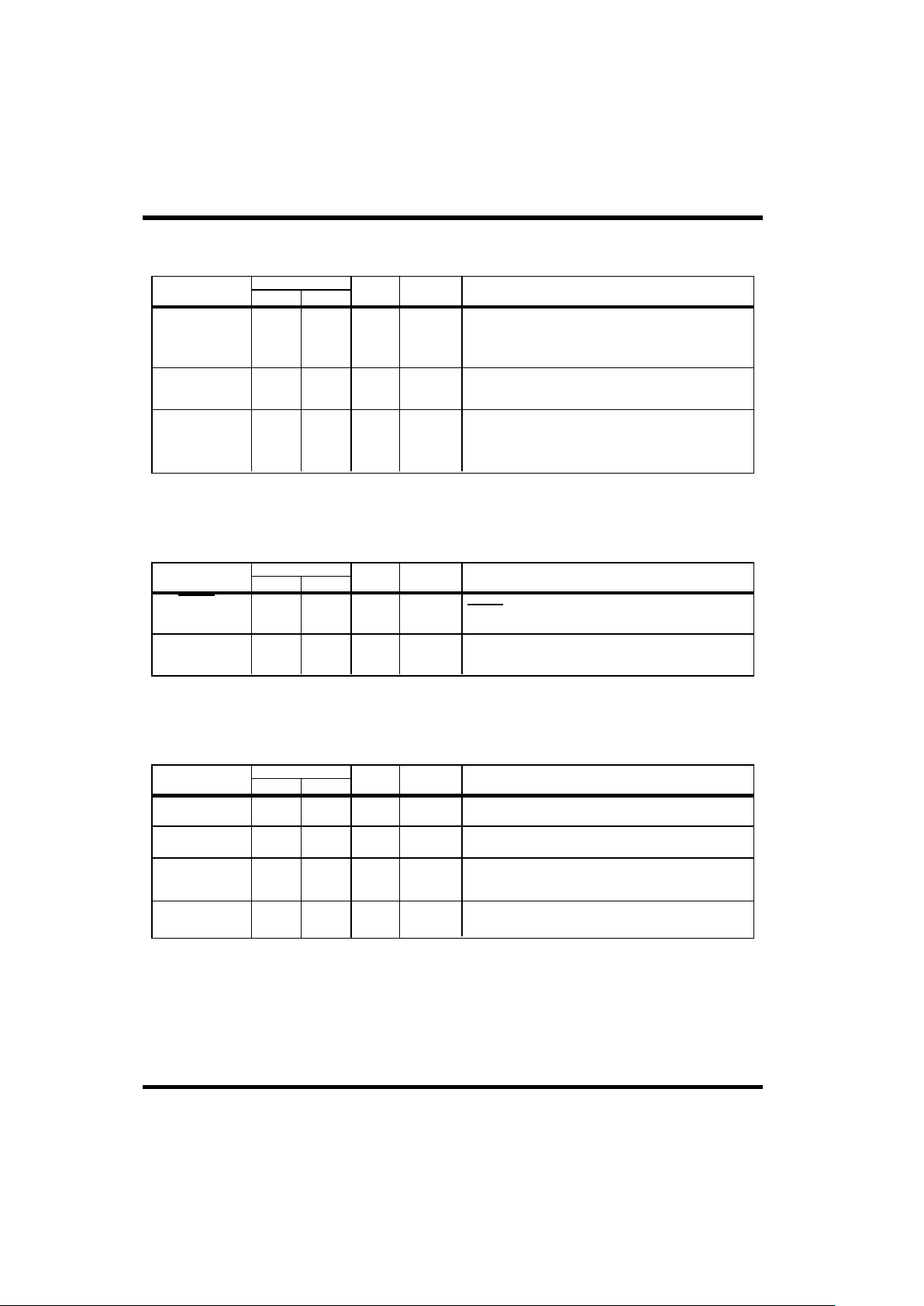
Since the RTMP’s architecture is based on a series of data
pointers, the 1553 transmit and receive data can be placed
anywhere in the 64K memory space, allowing the system
designer to optimize memory usage. The system designer
can program the RTMP to store the data received over the
1553 bus in one of two ways. The RTMP can store the
received data in a single data buffer or in separate buffers.
When the RTMP stores the received data in a single buffer,
all received data, regardless of subaddress, is stored in
contiguous locations in the shared memory. When the
RTMP stores the received data in separate buffers, the
RTMP stores the data associated with each of the 30
subaddresses in unique locations in memory.
The RTMP has six internal registers that provide the host
subsystem with RTMP control and status information.
Three of these registers are read/write: Time Tag Data
Register (TTD), the Control Register (CTL), and the Base
Pointer Data Register (BPD). Two are read only:
Operational Status Register (OPS), and the Last Command
Register (LCM). The Stop Self-Test Register (SST) is a
write-only register. To control the RTMP and the 1553
interface, the host begins by programming the Base Pointer
Data Register. By programming the BPD, the system
designer tells the RTMP where in the shared memory the
64-word Pointer Block will reside, whether the RTMP will
store the 1553 received data in single or separate buffers,
and how deep these data buffers will actually be. Figure 3
is a simple representation of the RTMP’s memory-mapping
architecture.
After the host has programmed the BPD, the 1553 interface
is enabled by setting either CHAEN or CHBEN in the
RTMP’s Control Register. The RTMP now monitors the
1553 data bus for a valid command word or mode code to
its particular terminal address. When received, the RTMP
looks at the mode bit (single/separate) in the BPD, the 1553
command transmit/receive bit, and the mode code or
subaddress portion of the 1553 command to determine
which of the address pointers in the 64-word Pointer Block
the RTMP will use for this particular memory transaction.
Each memory transaction consists of memory writes for
receive command words and memory reads for transmit
command words. This process continues until all 1553 data
words have been received or transmitted. If the host has
enabled any of the RTMP’s interrupts, the RTMP asserts
them when the memory transaction is complete.
Page 4
RTMP-4
ADDRESS BUS
DATA BUS
CONTROL
1553 TRANSCEIVER
UT1553 RTMP
HOST
SUBSYSTEM
64K x 16
SHARED RAM
1553 BUS A
1553 BUS B
UT63M125
Figure 2. RTMP General System Diagram
LSB
BUFFER MODE SELECT
L
S
F
U
B
1
Z
I
S
B
2
Z
I
S
B
0
Z
I
S
B
3
Z
I
S
B
64K x 16
SHARED RAM
0000H
FFFFH
BASE POINTER
DATA REGISTER
B
P
A
6
THESE TEN BITS FORM THE ADDRESS
OF THE STARTING LOCATION OF THE
64-WORD POINTER BLOCK.
64-WORD
POINTER BLOCK
RECEIVE DATA
POINTER (30)
TRANSMIT DATA
POINTER (30)
RECEIVE SUBADDRESS
DATA BUFFER -
8 TO 32K WORDS
TRANSMIT SUBADDRESS
DATA BUFFER
THE RECEIVE DATA BUFFER SIZE
IS PROGRAMMED WITH THESE FOUR BITS.
MSB
Figure 3. RTMP Receiveand Transmit Data Memory Mapping
Page 5
RTMP-5
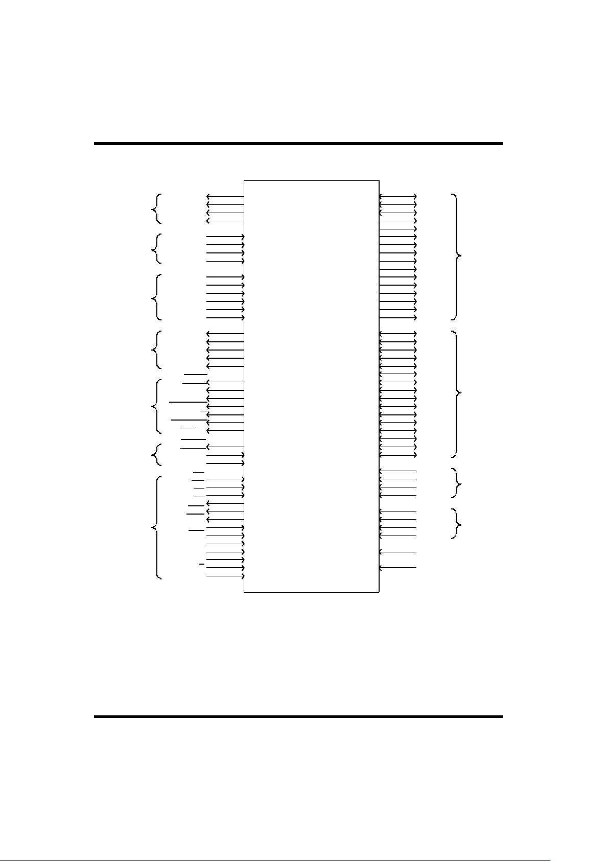
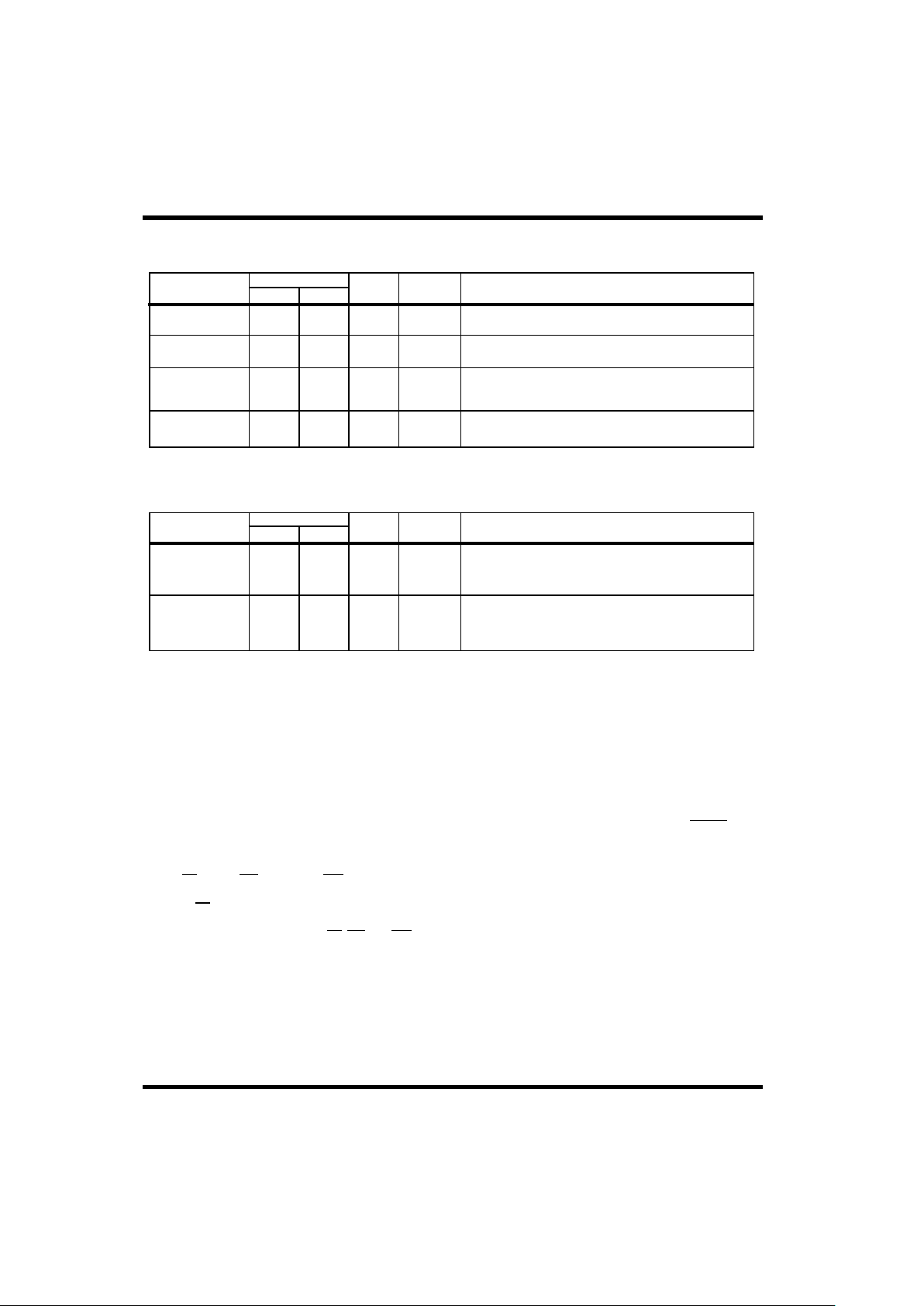
2.0 PIN IDENTIFICATION AND DESCRIPTION
Bidirectional pin.
Leadless chip carrier pinnumbers are not in parentheses.
( ) Pingrid array pin numbers are in parentheses.
(F3)
(L5)
(F10)
(A7)
(K11)
(L11)
(L2)
(K2)
(K3)
(G11)
(J6)
(G10)
(A2)
(B11)
(C11)
(C10)
(E9)
(E10)
(E11)
(E3)
(A5)
(F9)
(L7)
(C1)
(D2)
(D1)
(F2)
(E2)
(D10)
(D11)
(F11)
(B4)
(A4)
(A6)
(B5)
(C5)
(C6)
(B6)
(B7)
(C7)
(A8)
(B8)
(A9)
(A10)
(B9)
(B10)
(A11)
(L1)
(J2)
(K1)
(J1)
(H2)
(H1)
(G3)
(G2)
(G1)
(F1)
(E1)
(J5)
(H11)
(K8)
(L9)
(G9)
(H10)
(J11)
(K5)
(K6)
(L4)
(K4)
(L3)
(B3)
(A3)
(A1)
(B2)
(C2)
(B1)
(J7)
(K9)
(L10)
(K7)
(L6)
(J10)
(K10)
(L8) A
A
A
A
A
A
A
A
A
A
A
A
A
A
A
A
0
1
2
3
4
5
6
7
8
9
10
11
12
13
14
15
D
D
D
D
D
D
D
D
D
D
D
D
D
D
D
D
0
1
2
3
4
5
6
7
8
9
10
11
12
13
14
15
ADDRESS
LINES
DATA
LINES
TAZ
TAO
TBZ
TBO
RAZ
RAO
RBZ
RBO
RTA0
RTA1
RTA2
RTA3
RTA4
RTPTY
MCSA0
MCSA1
MCSA2
MCSA3
MCSA4
BIPHASE
OUT
BIPHASE
IN
MODE CODE/
SUBADDRESS
STATUS
SIGNALS
TERMINAL
ADDRESS
DMA
SIGNALS
CONTROL
SIGNALS
POWER
GROUND
CLOCK
RESET
CLK
14
12
13
41
22
40
72
51
50
52
44
46
45
49
48
47
21
38
28
29
39
37
36
19
18
17
16
15
71
73
74
75
76
77
33
34
23
25
30
31
26
27 70
69
68
67
65
64
63
61
60
59
58
57
56
55
54
53
11
10
9
8
7
6
5
4
3
2
83
82
81
80
79
78
24
43
66
84
1
20
42
62
35
32
++
++
++
++
***Pin internally pulled up.
Pin internally pulled down.
EORT
EOMC
MERR
TIMERON
CHA/B
COMSTR
MC /SA
DMAR
*DMAG
*DMAEN
RD
WR
*CS
AV
RRD
RWR
**TAPEN
*SVC
**ILLCOM
**SME
**ENBC
PRA/B
**TEST
V
SS
V
DD
V
DD
V
DD
V
DD
V
SS
V
SS
V
SS
RESET
Figure 4. RTMP Functional Pin Description
Page 6

RTMP-6
Legend for TYPE and ACTIVE fields:
TO = TTL output
I = TTL input
TUI = TTL input (pull-up)
TDI = TTL input (pull-down)
TTO = Three-state TTL output
TTB = Three-state TTL bidirectioal
AH =Active high
AL = Active low
D15 78 C1 TTB Bit 15 (MSB) of the bidirectional Data bus.
DATA BUS
NAME
PIN NUMBER
LCC PGA
TYPE ACTIVE DESCRIPTION
D14
D13
D12
D10
D9
D8
D7
D6
D5
D4
D3
D2
D1
D0
79
80
81
82
83
2
3
4
5
6
7
8
9
10
11
D2
D1
F2
E2
E1
F1
G1
G2
G3
H1
H2
J1
K1
J2
L1
TTB
TTB
TTB
TTB
TTB
TTB
TTB
TTB
TTB
TTB
TTB
TTB
TTB
TTB
TTB
Bit 14 of the bidirectional Data bus.
Bit 13 of the bidirectional Data bus.
Bit 12 of the bidirectional Data bus.
Bit 11 of the bidirectional Data bus.
Bit 10 of the bidirectionalData bus.
Bit 9 of the bidirectional Data bus.
Bit 8 of the bidirectional Data bus.
Bit 7 of the bidirectional Data bus.
Bit 6 of the bidirectional Data bus.
Bit 5 of the bidirectional Data bus.
Bit 4 of the bidirectional Data bus.
Bit 3 of the bidirectional Data bus.
Bit 2 of the bidirectional Data bus.
Bit 1 of the bidirectional Data bus.
Bit 0 (LSB) of the bidirectional Data bus.
D11
--
--
--
--
--
--
--
--
--
--
--
--
--
--
--
--
Page 7
RTMP-7
A15 53 A11 TTO Bit 15 (MSB) of the Address bus.
ADDRESS BUS
NAME
PIN NUMBER
LCC PGA
TYPE ACTIVE DESCRIPTION
A14
A13
A12
A10
A9
A8
A7
A6
A5
A4
A3
A2
A1
A0
TTO
TTO
TTO
TTO
TTO
TTO
TTO
TTO
TTO
TTO
TTO
TTO
TTB
TTB
TTB
Bit 14 of the Address bus.
Bit 13 of the Address bus.
Bit 12 of the Address bus.
Bit 11 of the Address bus.
Bit 10 of the Address bus.
Bit 9 of the Address bus.
Bit 8 of the Address bus.
Bit 7 of the Address bus.
Bit 6 of the Address bus.
Bit 5 of the Address bus.
Bit 4 of the Address bus.
Bit 3 of the Address bus.
Bit 1 of the Address Bus. (Reference A2)
Bit 0 (LSB) of the Address Bus. (Reference A2)
A11
54
55
56
57
58
59
60
61
63
64
65
67
68
69
70
B10
B9
A10
A9
B8
A8
C7
B7
B6
C6
C5
B5
A6
A4
B4
--
--
--
--
--
--
--
--
--
--
--
--
--
--
--
--
Bit 2 of the Address bus. Address bits A2 - A0 are
bidirectional so the host can select one of the RTMP’s internal
registers during internal I/O operations.
47 F11 TO
NAME
PIN NUMBER
LCC PGA
TYPE ACTIVE DESCRIPTION
DMA SIGNALS
AL DMA Request. Indicates the RTMP is requesting
DMAEN
48
49
D11
D10
TUI
TUI
AL
AH
use of the Data bus from the current bus master.
DMA Enable. When high, this input allows the
RTMP to recognize DMAG. When low, DMAEN places all
three-state pins in a high-impedance state and disables the
RTMP’s memory access cycle.
DMA Grant. Gives control of the Data bus to the RTMP.
DMAG is recognized only if DMAEN is high. DMAG must
remain asserted until AV goes high to ensure that the RTMP
completes the current DMA cycle.
DMAG
DMAR
Page 8
RTMP-8
SME
ILLCOM
44 E9 TUI
NAME
PIN NUMBER
LCC PGA
TYPE ACTIVE DESCRIPTION
AL
45
46
52
50
51
40
E11
E10
C10
C11
B11
G10
TI
TI
TTO
TTO
TTO
TUI
AL
AL
AL
AL
AL
AL
Set Message Error. Asserting this input causes the
Message Error bit in thestatus word to be set.
Illegal Command. This input illegalizes a command
word that the RTMP accepts but the system does not
support. When set, the RTMP responds with the
Message Error bit set in the status word. ILLCOM
4122G11
J6
TDI
TDIAHAH
CONTROL SIGNALS
12 K2 TI
--
13
14
K3L2TDI
TDIAHAH
ENBC
TEST
Enable Broadcast. A high on this input, when the
RTMP is in the 1553B mode, allows the RTMP to
recognize a broadcast command word.
is used in conjunction with the Mode Code/
Subaddress outputs.
CS
RD
WR
AV
RRD
RWR
SVC
PRA/B
Chip Select. This input, along with RD and WR, allows
the host to access the RTMP’s internal data registers.
Read. When used in conjunction with CS, RD allows the
RTMP to place data from the selected internal register on the
Data bus (D15-D0).
Write. When used in conjunction with CS, WR latches data
from the Data bus (D15-D0) into the selected RTMP internal
register.
Address Valid. The RTMP asserts AV to indicate that the
address (A15-A0) is valid.
RAM Read. The RTMP asserts RRD during DMA cycles
that require data from system RAM.
RAM Write. The RTMP asserts RWR during DMA cycles
to write data to system memory.
Superseding Valid Command. The host system uses this
input when more than one RT is present in the system; i.e.,
a quad-redundant system. When asserted, this input causes
the RTMP to terminate all present activity and perform an
internal reset of encoders/decoders, RT state machine, and
DMA state machine. Registers are not affected. Do not assert
while DMAR is asserted (tpw 250ns minimum).
Program A/ B. This input is the 1553 mode select input. A high
input places the RTMP in the MIL-STD-1553A mode; a low
places the RTMP in the MIL-STD-1553B mode.
Test. The TEST input pin allows the user to select between
internal (TEST = 0) or external (TEST = 1) self-test. When
TEST equals a logic one and DMAEN equals a logic zero,
MCSA (4:0) and MC/SA three-state.
Page 9
RTMP-9
36 J11 TTO
NAME
PIN NUMBER
LCC PGA
TYPE ACTIVE DESCRIPTION
AL
STATUS SIGNALS
MERR
37
38
39
28
29
H10
H11
G9
K8
L9
TTO
TO
TO
TO
TO
AL
AL
AH
--
AL
21 J5 TTO
NAME
PIN NUMBER
LCC PGA
TYPE ACTIVE DESCRIPTION
AL
MCSA0
MCSA1
MCSA2
MCSA3
MCSA4
15
16
17
18
19
L3
K4
L4
K6
K5
TTO
MODE CODE/SUBADDRESS
Timer On. Indicates the RTMP is transmitting data.
The output remains active until the data transmission is
complete or the internal fail-safe timer times out (600ms
for 1553A and 800ms for 1553B). The RTMP internally
disables both transmitters and keeps them disabled until the
RTMP receives a valid command word. This signal is asserted approximately 250ns
before beginning of status word transmission.
--
End of Receive/Transmit. This interrupt is a pulse that is
maskable by writing to the Control Register. The user can
select EORT to occur at the end of receive command activity,
at the end of transmit command activity, under either of these
conditions, or disable it completely. The EORT output is designed to simulate an open-collector output and requires a
pull-up resistor. (250ns pulse width). This signal is not generated if a message error condition exists.
EORT
End of Mode Code. this non-maskable interrupt is a pulse that
occurs at the end of all memory accesses associated with any
mode code command. The EOMC output is designed to simulate an open-collector output and requires a pull-up resistor.
EOMC and EORT can be logically ORed together to form a
composite interrupt. The 250ns pulse width is generated after
command word is stored. This signal is not generated if a
message error condition exists.
EOMC
COMSTR
CHA/ B
TIMERON
Message Error. Active when the RTMP detects an error in
the 1553 transmission and sets the Message Error bit in the
status word. MERR is reset when the RTMP receives the next
valid command word. (COMSTR assertion)
Channel A/ B. When high, this output indicates the RTMP
received the last command on Channel A; when low, the last
command was received on Channel B.
Mode Code/Subaddress. MC/SA = 0 indicates that the MCSAO-MCSA4 pins contain the Mode Code bits of the most
recently received mode code. MC /SA = 1 indicates that
MCSA0-MCSA4 pins contain the Subaddress bits of the
most recently received command word.
MC /SA
Mode Code/Subaddress. These five bits are used in conjunction with the MC/SA output. MC/SA = 0 indicates that these
five bits are the five least significant bits of the mode code
command word. MC /SA = 1 indicates these five bits are the
1553 command word subaddress.
Command Strobe. This low-going pulse identifies receipt of a valid 1553 command word.
Page 10
RTMP-10
RTA4 73 B3 TI
NAME
PIN NUMBER
LCC PGA
TYPE ACTIVE DESCRIPTION
Remote Terminal Address Inputs. The RTMP uses
REMOTE TERMINAL ADDRESS
these inputs to select the terminal address for this
specific remote terminal.
Terminal Address Parity Enable. Enables the
RTMP’s Terminal Address parity-checking
Remote Terminal Parity. When the Terminal
Address parity-checking function is enabled
(TAPEN = 1), RTPTY must provide odd parity
for the terminal address input pins (RTA4-RTA0).
RTA3
RTA2
RTA1
RTA0
TAPEN
RTPTY
74
75
76
77
72
71
A1
B2
C2
B1
A2
A3
TDI
TI
AH
32 L11 TI
NAME
PIN NUMBER
LCC PGA
TYPE ACTIVE DESCRIPTION
MASTER RESET AND CLOCK
RAO 23 L6 TI
NAME
PIN NUMBER
LCC PGA
TYPE ACTIVE DESCRIPTION
Receiver (Channel) A One. Manchester input from
CHANNEL A BIPHASE SIGNALS
AL
CLK 35 K11 TI
the 1553 bus receiver.
Receiver (Channel) A Zero. This input is the
complement of RAO.
Transmitter (Channel) A One. This Manchester-
encoded data output is connected to the 1553 bus
transmitter input. The output is idle low.
Transmitter (Channel) A Zero. This output is
the complement of TAO. The output is idle low.
RAZ
TAO
TAZ
25
26
27
K7
J7
L8
TI
TO
TO
function.
--
--
--
--
--
--
--
RESET
Reset. Initializes all internal functions of the RTMP.
RESET must be asserted before normal RTMP operation.
Clock. The clock input requires a 50% ± 10% duty cycle
with an accuracy of 12MHz ± 0.01%.
Page 11
RTMP-11
3.0 REMOTE TERMINAL ARCHITECTURE
3.1 Internal Registers
The RTMP has six internal registers that allow the host to
control the RTMP’s actions and also to obtain its operational
status. The host can read from or write to three of these
registers: the Time Tag Data Register (TTD), the Control
Register (CTL), and the Base Pointer Data Register (BPD).
Two of the registers are read-only: the Operational Status
Register (OPS), and the Last Command Register (LCM).
The Stop Self-Test Register (SST) is a write-only register.
Six signals allow the host to access the RTMP’s internal
registers. Three of the six signals are control signals: Chip
Select (CS), Read (RD ), and Write (WR). The other three
signals are the RTMP’s bidirectional address lines, A0 - A2.
When the CS = 0, the three least significant address lines,
A0 - A2, become inputs to the RTMP. The RTMP decodes
these three address lines, along with CS, RD , and WR, to
determine which of the six internal registers the host is
attempting to access. Table 1 shows the addresses for the
RTMP’s internal registers for read and write operations.
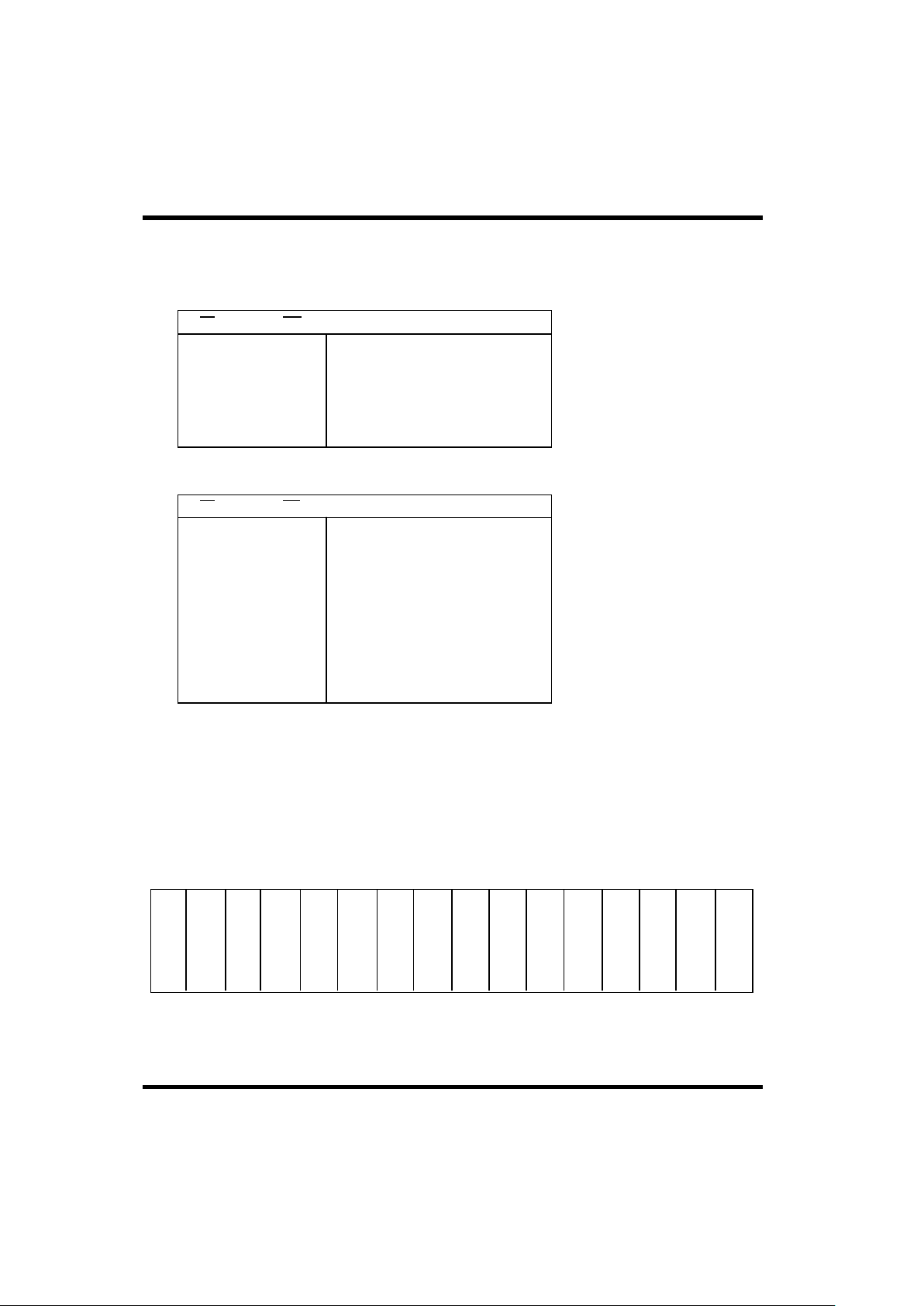
3.2 Read/Write Registers
The RTMP has three internal read/write registers. These
three registers are:
• The Time Tag Data Register
• The Control Register
• The Base Pointer Data Register
Time Tag Data Register (TTD)
The TTD contains a free-running, 16-bit, ripple counter.
The Time Tag clock has a resolution of 64ms. The TTD is
initialized to 0000H when the host asserts the RESET input.
All TTD bits are programmable by performing a write to
the TTD with the desired bit pattern.
The RTMP stores the TTD’s value in the shared memory
area at the end of each 1553 receive message. The host can
also directly read the TTD. Since the TTD is a free-running
counter, the host may read the TTD while the counter is
rippling, resulting in the host reading erroneous data. If this
situation presents a problem, the host should read the TTD
data twice. Figure 5 represents the TTD. (0000H after
Master Reset.)
RBO 33 K10 TI
NAME
PIN NUMBER
LCC PGA
TYPE ACTIVE DESCRIPTION
Receiver (Channel) B One. Manchester data input
CHANNEL B BIPHASE SIGNALS
from the 1553 bus receiver.
Receiver (Channel) B Zero. This input is the
complement of RBO.
Transmitter (Channel) B One. This Manchester-
encoded output is connected to the 1553 bus
transmitter input. The output is idle low.
Transmitter (Channel) B Zero. This output is the
complement of TBO. The output isidle low.
RBZ
TBO
TBZ
34
30
31
J10
L10
K9
TI
TO
TO
24 L7
NAME
PIN NUMBER
LCC PGA
TYPE ACTIVE DESCRIPTION
POWER AND GROUND
43
66
84
1
20
42
62
F9
A5
E3
F3
L5
F10
A7
--
--
--
--
--
--
--
--
+5 VDC Power. Power supply input must be
Reference Ground. Zero VDC logic ground.
V
DD
V
SS
Page 12
RTMP-12
Table 1. RTMP Internal Register Addresses
1. RTMP Register Write Addresses
A2 A1 A0
0
0
0
0
0
0
0
0
0
0
0
0
0
0
1
1
0
1
0
1
Time Tag Data Register
Control Register
Base Pointer Data Register
Stop Self-Test Register
2. RTMP Register Read Addresses
A2 A1 A0
0
0
0
0
0
0
0
0
0
0
0
0
0
0
1
0
0
1
1
0
0
1
0
1
0
Time Tag Data Register
Control Register
Base Pointer Data Register
Operational Status Register
Last 1553 Command Register
0 0 1 X X Don’t Care
0
0
0
0
0
0
1
1
1
0
1
1
1
0
1
Don’t Care
Don’t Care
Don’t Care
CS WR
CS RD
15 14 13 12 11 10 9 8 7 6 5 4 3 2 1 0
C
N
T
1
5
C
N
T
1
4
C
N
T
1
3
C
N
T
1
2
C
N
T
1
1
C
N
T
1
0
C
N
T
9
C
N
T
8
C
N
T
7
C
N
T
6
C
N
T
5
C
N
T
4
C
N
T
3
C
N
T
2
C
N
T
1
C
N
T
0
MSB LSB
Figure 5. The Time Tag Data Register
Page 13

RTMP-13
3.4 Control Register (CTL)
The CTL provides the host with the ability to control four functions: (1) programming the bits in 1553 status word; (2) masking
the End of Receive/Transmit message activity interrupt (output pin EORT ); (3) enabling and selecting the channel for the selftest; and (4) selecting the active 1553 channel. The definition of the 1553 status word bits in the CTL is different when the
RTMP is operating in the 1553A mode (PRA/B = 1) as opposed to the1553B mode (PRA/B = 0). Figure 6 shows the bit
definitions in the CTL for the 1553A mode; figure 7 shows the definition for the 1553B mode.
The host determines the CTL functions status by reading the CTL Register.
CTL Bit Definitions - 1553A Mode
Bit 15 CHAEN [0] Channel A Enable. When CHAEN = 1, the RTMP responds to a 1553 command word or mode
code on bus Channel A. CHAEN = 0 disables the RTMP from responding to 1553 command word
or mode code on 1553 bus Channel A.
Bit 14 CHBEN [0] Channel B Enable. When CHBEN = 1, the RTMP responds to a 1553 command word or mode
code on bus Channel B. CHBEN = 0 disables the RTMP from responding to 1553 command word
or mode code on 1553 bus Channel B. Disable for internal self-test.
Bit 13 STEN [0] Self-Test Enable. STEN enables the RTMP’s internal self-test.
Bit 12 STCS [0] Self-Test Channel Select. If the host has enabled an RTMP self-test (STEN = 1), STCS selects
the RTMP receiver channel to test. STCS = 1 selects Channel A, and STCS = 0 selects Channel B.
Bit 11 IM1 [0] Interrupt Mask One. If IM1 = 1, the EORT interrupt output is active at the end of 1553 receive
command memory activity. IM1 = 0 masks this interrupt function.
Bit 10 IM2 [0] Interrupt Mask Two. If IM2 = 1, the EORT interrupt output is active at the end of 1553 transmit
command memory activity. IM2 = 0 masks this interrupt function.
Bit 9 SWB10 [0] Status Word Bit 10. When the host sets this bit, SWB10 = 1, the bit in the RTMP’s status word
that is transmitted during bit time ten is set (see figure 30 for status word bit time definitions).
The bits in the status word are system-defined in MIL-STD-1553A.
Bit 8 SWB11 [0] Status Word Bit 11. When the host sets this bit (SWB11 = 1), the bit in the RTMP’s status word
transmitted during bit time 11 is set.
Bit 7 SWB12 [0] Status Word Bit 12. When the host sets this bit (SWB12 = 1), the bit in the RTMP’s status word
transmitted during bit time 12 is set.
Bit 6 SWB13 [0] Status Word Bit 13. When the host sets this bit (SWB13 = 1), the bit in the RTMP’s status word
transmitted during bit time 13 is set.
Bit 5 SWB14 [0] Status Word Bit 14. When the host sets this bit (SWB14 = 1), the bit in the RTMP’s status word
transmitted during bit time 14 is set.
Bit 4 SWB15 [0] Status Word Bit 15. When the host sets this bit (SWB15 = 1), the bit in the RTMP’s status word
transmitted during bit time 15 is set.
Bit 3 SWB16 [0] Status Word Bit 16. When the host sets this bit (SWB16 = 1), the bit in the RTMP’s status word
transmitted during bit time 16 is set.
Bit 2 SWB17 [0] Status Word Bit 17. When the host sets this bit (SWB17 = 1), the bit in the RTMP’s status word
transmitted during bit time 17 is set.
Bit 1 SWB8 [0] Status Word Bit 18. When the host sets this bit (SWB18 = 1), the bit in the RTMP’s status word
transmitted during bit time 18 is set.
Bit 0 TFLG Terminal Flag. TFLG = 1 sets the Terminal Flag bit in the 1553A status word. TFLG = 0 resets
the Terminal Flag bit in the 1553A status word.
Page 14

RTMP-14
CTL Bit Definitions - 1553B Mode
Bit 15 CHAEN [0] Channel A Enable. Same as 1553A mode. Disable for internal self-test.
Bit 14 CHBEN [0] Channel B Enable. Same as 1533A mode. Disable for internal self-test.
Bit 13 STEN [0] Self-Test Enable. Same as 1553A mode.
Bit 12 STCS [0] Self-Test Channel Select. Same as 1553A mode.
Bit 11 IM1 [0] Interrupt Mask One. Same as 1553A mode.
Bit 10 IM2 [0] Interrupt Mask Two. Same as 1553A mode.
Bit 9 INSTR [0] Instrumentation Bit. When INSTR = 1, the RTMP’s 1553 status word response has the Instru-
mentation bit set. This bit remains set until INSTR is set to 0.
Bit 8 SVREQ [0] Service Request Bit. When SVREQ = 1, the RTMP’s 1553 status word response has the Service
Request bit set. This bit remains set until SVREQ is set to 0.
Bit 7 N/A This bit is defined as a reserved bit in MIL-STD-1553B and is not used. Setting this bit has no
effect on the status word response.
Bit 6 N/A Same as bit 7.
Bit 5 N/A Same as bit 7.
Bit 4 BDCST [0] Broadcast Bit. When BDCST = 1, the RTMP’s 1553 status word response has the Broadcast bit
set. Manual override; not cleared by receipt of next command. Broadcast bit in outgoing status
word is set to a logical one on the receipt of broadcast command.
Bit 3 BUSY [0] Busy Bit. When BUSY = 1, the RTMP’s 1553 status word response has the Busy bit set. This bit
remains set until is set to 0.
Bit 2 SFLG [0] Subsystem Flag. When SFLG = 1, the RTMP’s 1553 status word response has the Subsystem
Flag bit set. This bit remains set until SFLG is set to 0.
Bit 1 N/A Same as bit 7.
Bit 0 TFLG [0] Terminal Flag. Same as 1553A mode.
15 14 13 12 1110 9 8 7 6 5 4 3 2 1 0
C
H
A
E
N
C
H
B
E
N
S
T
E
N
S
T
C
S
I
M
1
I
M
2
S
W
B
1
T
F
L
G
Figure 6. The Control Register in 1553A Mode
MSB LSB
15 14 1312 11 10 9 8 7 6 5 4 3 2 1 0
N
/
A
B
U
S
Y
T
F
L
G
Figure 7. The Control Register in 1553B Mode
MSB LSB
0
S
W
B
1
1
S
W
B
1
2
S
W
B
1
3
S
W
B
1
4
S
W
B
1
5
S
W
B
1
6
S
W
B
1
7
S
W
B
1
8
C
H
A
E
N
C
H
B
E
N
S
T
E
N
S
T
C
S
I
M
1
I
M
2
I
N
S
T
R
S
V
R
E
Q
N
/
A
N
/
A
B
D
C
S
T
S
F
L
G
N
/
A
Page 15

RTMP-15
3.5 Base Pointer Data Register
The BPD provides three types of information: (1) the location in memory for the 64-word Pointer Block; (2) the receive-data
storage-buffer select for either single or separate data buffers; and (3) the size or depth of the single or separate data buffers
(figure 8). (0000H after Master Reset.)
BPD Bit Definitions
Bit 15- BPA15-BPA 6 Block Pointer Address. These ten bits provide the RTMP with the Bit 6 ten most significant address
lines for the location, within the 64K word addressing range, of the 64-word Pointer Block.
Bit 5 N/A This bit is not used.
Bit 4 BUFSL Buffer Select. When BUFSL = 1, the host selects the RTMP’s single buffer mode of storing 1553
receive data. If BUFSL = 0, the host selects the separate buffer mode of storing 1553 receive data.
Bit 3- BSIZ3-BSIZ0 Buffer Size Select. These four bits select the size of the receive data Bit 0 buffers and can range
from 3 (0011B) to 15 (1111B). The actual size of the data buffer is equal to 2x where X is the
decimal equivalent of BSIZ3-BSIZ0. The size of the data buffers can range from eight (23) words
to 32K (215) words. The variable X is not defined for zero through two.
3.6 Read Only Registers
The RTMP has two internal registers that are read-only. These two registers provide status information on the operation of the
RTMP:
• The Operational Status Register
• The Last 1553 Command Register
15 14 13 12 11 10 9 8 7 6 5 4 3 2 1 0
B
P
A
1
5
1
4
131
2
1
1
1
0
9 8 7 6
N
/
A
MSB LSB
B
P
A
B
P
A
B
P
A
B
P
A
B
P
A
B
P
A
B
P
A
B
P
A
B
P
A
S
L
B
U
F
Z
3
B
S
I
Z
2
B
S
I
Z
1
B
S
I
Z
0
B
S
I
Figure 8. The Base Pointer Data Register
Page 16

RTMP-16
3.6.1 Operational Status Register (OPS)
The OPS provides the host with the operational status of the RTMP while the RTMP is active. Figure 9 shows the information
bits stored in the OPS.
OPS Bit Definitions
Bit 15 MACT [0] Message Active. MACT = 1 indicates that the RTMP is actively processing a message. The RTMP
clears MACT upon completing the message.
Bit 14 VMPRO [0] Valid Message Processed. VMPRO = 1 indicates that the RTMP has processed a valid 1553
message. The host clears VMPRO bit when the OPS is read.
Bit 13 ME [0] Message Error. ME = 1 indicates that a 1553 message error has occurred. The host clears ME
when the OPS is read unless the condition that caused the MERR still persists after the register
read.
Bit 12 PE [X] Parity Error. PE = 0 indicates that the RTMP has detected an error in the Terminal Address parity.
This bit can only be active when TAPEN = 1.
Bit 11 STACT [0] Self-Test Active. STACT = 1 indicates that the RTMP is performing a built-in self-test.
Bit 10 BDCEN [X] Broadcast Enable. BDCEN = 1 indicates that the RTMP will accept a 1553 broadcast command
as a valid command.
Bit 9 TFGEN [1] Terminal Flag Enable. When the RTMP is in the 1553B mode, TFGEN = indicates that the
Terminal Flag option is set. Mode code 00110 (Inhibit Terminal Flag) will clear this bit.
Bit 8 CHAEN [0] 1553 Channel A Enable. CHAEN = 1 indicates that Channel A is enabled and ready to process
1553 bus messages.
Bit 7 CHBEN [0] 1553 Channel B Enable. CHBEN = 1 indicates that Channel B is enabled and ready to process
1553 bus messages.
Bit 6 MSEL [X] Mode Select. When MSEL = 1, the RTMP is in the 1553A mode of operation. MSEL = 0 indicates
the RTMP is in the 1553B mode of operation.
Bit 5 MDRCV [0] Mode Received. MDRCV = 0 indicates that the last valid 1553 command the RTMP received
was a mode command.
Bit 4 XMTAC [0] Transmitter Active. XMTAC = 1 indicates that the RTMP’s transmitter is transmitting data.
Bit 3 ILCMD [X] Illegal Command. ILCMD = 1 indicates that the last 1553 command the RTMP received was
illegal. ILCMD is cleared when the host reads the OPS. In 1553A mode, this bit reflects input pin
ILLCOM. In 1553B mode, this bit reflects either input pin ILLCOM or internal hardware. Internal
illegalization is reviewed in table 2.
Bit 2 CHA/B [0] Channel A or . CHA/B = 1 indicates that the last valid 1553 command word the RTMP received
was on Channel A. CHA/B = 0 indicates that the last valid command word was on Channel B.
Bit 1 VCMD [0] Valid 1553 Command. VCMD = 1 indicates that the last command word the RTMP received was
valid. VCMD is reset when the host reads the OPS.
Bit 0 OE [0] Overrun Error (Framing Error). OE = 1 indicates that the RTMP has detected an overrun error.
This bit is reset when the host performs an OPS read unless the error condition persists.
15 14 13 12 11 10 9 8 7 6 5 4 3 2 1 0
M
A
C
C R
O
CTE
N
L
MSB LSB
V
M
P
MEPES
T
A
B
D
C
M
S
E
A
C
X
M
T
M
D
I
L
C
/
B
C
H
A
D
V
C
M
0
E
E
N
T
F
G
E
N
A
C
H
E
N
B
C
H
C
V
M
D
R
Figure 9. The Operational Status Register
Page 17

RTMP-17
3.6.2 Last 1553 Command Register (LCM)
The RTMP stores the last valid 1553 command word it
received in the LCM. The only exception is if the RTMP is
in the 1553B mode and it receives a Transmit Last
Command Word mode code. Figure 10 shows the
configuration of the LCM. (0410H after Master Reset.)
3.7 Write Only Register
The RTMP has one register that is write only. This register
is the Stop Self-Test Register (SST). The host can terminate
the RTMP’s self-test execution by writing to the SST. When
the host performs a write to the SST, the RTMP terminates
all memory activity. The Self-Test Enable (STEN) bit in the
CTL is also reset, and the Self-Test Active (STACT) bit in
the OPS is reset. When writing to the SST, the 16-bit data
word is a Don’t Care.
4.0 REMOTE TERMINAL INTERFACE
OPERATION
The RTMP’s remote terminal interface is based on a shared
memory concept where the shared memory is the link
between the MIL-STD-1553 data bus and the host
subsystem (figure 11). All 1553 data, whether transmitted
or received, must at one time be stored in this defined
memory area. The RTMP accesses the shared memory area
with a conventional Direct Memory Access (DMA)
interface.
Since the RTMP can access data anywhere within the 64K
memory space, the host has to specify exactly where in
memory the data associated with each valid transmit or
receive command word or mode code is located. The host
specifies the 1553 data area locations by programming the
RTMP’s Base Pointer Data Register (BPD) and by
initializing the 64-word Pointer Block. The BPD tells the
RTMP where in memory the Pointer Block is located. The
Pointer Block in turn specifies the location in memory where
the data associated with each valid command word or mode
code resides.
Therefore, to control the RTMP’s operation, the host first
programs the BPD to provide the RTMP with three essential
pieces of information: (1) the location in memory of the 64word Pointer Block; (2) the type of data buffer -- single or
separate; and (3) the receive data buffer size. The host can
update the Base Pointer Data Register if a new 64-word
Pointer Block needs to be selected, but do not update the
BPD while the RTMP is processing a message transaction.
Figure 8 shows the BPD.
4.1 Programming the BPD
The host programs the ten most significant bits of the BPD
(BPA15 - BPA6) to point to the starting address of the 64word Pointer Block within the RTMP’s 64K address space.
The RTMP generates the least significant six address lines
to determine which of the words within the 64-word Pointer
Block to use for a specific 1553 transmission. The RTMP
does this by detecting the T/ R bit and the subaddress bits of
the last 1553 command word (figure 12). Usually the six
least significant address lines, BPA5-BPA0, are part of the
T/R bit and subaddress or mode code bits of the last
command word, respectively. In some cases, BPA5-BPA0
are forced to specific values: (1) when the RTMP stores the
command word on the data buffer; (2) when the single buffer
mode of operation is chosen; and (3) when a mode code is
received.
The Data Buffer Mode bit, BUFSL, is the next bit in the
BPD that the host programs. The state of BUFSL determines
whether the RTMP stores the 1553 receive data in a single
data buffer (BUFSL = 1) or in separate data buffers (BUFSL
= 0).
Finally, the host programs bits BSIZ3-BSIZ0 in the BPD to
tell the RTMP how large to make the separate data buffers.
A formula determines the size of the data buffer(s): take the
decimal equivalent of the binary number represented by
BSIZ3-BSIZ0, where BSIZ3 is the MSB. This number,
represented by X, can range in size from three to fifteen.
The actual size of the data buffers is equal to 2. This means
the data buffers can range from 8 to 32K words in length.
In the single buffer mode, bits BSIZ3-BSIZ0 determine the
size of this single buffer. In the separate buffer mode, all
data buffers are the same size. This means the system
designer must program the buffer size so the largest possible
message the RTMP can receive over the 1553 bus fits within
the programmed buffer size.
4.2 RTMP Pointer Block
The RTMP’s Pointer Block is a contiguous block of 64, 16bit words. The RTMP uses this block of data as the actual
address pointer locations for the memory accesses
associated with each 1553 message transaction. Therefore,
the Pointer Block is divided into receive data pointers, of
which one location is for the single buffer mode, transmit
data pointers, a mode code command pointer location, and
a location for the current 1553 command word (figure 13).
The host must initialize the Pointer Block before enabling
the RTMP’s 1553 receivers
15 14 13 12 11 10 9 8 7 6 5 4 3 2 1 0
T
A
4
MSB LSB
T
/
R
S
A
4
T
A
3
T
A
2
T
A
1
T
A
0
S
A
3
S
A
2
S
A
1
S
A
0
W
C
4
W
C
3
W
C
2
W
C
1
W
C
0
X
Page 18

RTMP-18
The host can program the 16-bit pointer addresses that make
up the Pointer Block to point to any memory location in the
RTMP’s 64K memory space. In this respect, the host has
total flexibility to determine where in RAM it stores the
actual transmit, receive, and mode code data. The RTMP’s
data storage flexibility allows the host to buffer 1553 receive
messages and maintain data integrity.
The host can update the pointer data within the Pointer
Block at any time, but the recommended procedure is for
the host not to update the pointer data for 1553 receive
command data while the RTMP is actively processing a
message. To prevent this action, the host can program the
RTMP to generate an end-of-activity interrupt for every
valid 1553 message with associated data words. In addition,
the host can read the Operational Status Register to
determine if the RTMP is active.
The RTMP uses the present 1553 command word and the
selected mode of operation, single or separate mode, to
determine which pointer within the 64-word Pointer Block
to use as an address pointer for the memory accesses during
1553 message activity. The 1553 command word T/R Bit
and the subaddress bits, or the mode code bits for a mode
command, specify the exact location of the address pointer
in the Pointer Block for transmit, receive, and mode code
command words. If the host has selected the single mode of
operation, the RTMP forces selection of the address pointer
stored in the single mode location for all receive commands.
The RTMP stores the present command word in the first
ADDRESS BUS
DATA BUS
CONTROL
1553 TRANSCEIVER
UT1553 RTMP
HOST
SUBSYSTEM
1553 BUS A
1553 BUS B
64K x 16 SHARED
RAM
64-WORD
POINTER BLOCK
RECEIVE DATA
BUFFER(S)
TRANSMIT DATA
BUFFER(S)
THESE THREE BLOCKS CAN
UT63M125
RESIDE ANYWHERE IN THE
64K MEMORY SPACE.
Figure 11. The Memory Link between the RTMP and the Host Subsystem
Page 19

RTMP-19
4.3 Pointer Block Location Definitions
For the following description of the Pointer Block locations,
please refer to figure 13.
Command Word Data - Location 0-0H of the Pointer Block
contains the last valid 1553 command word the RTMP
received. Bit times 4 through 19 (figure 14) of the 1553
command word are stored in bit positions 15 through 0,
respectively. The RTMP updates this location with the most
recent command word except when the RTMP is in the
1553B mode and it receives a Transmit Last Command
mode code.
Separate Mode, Receive Data Pointers - Pointer Block
address locations 1-30 (01H-1EH) contain the pointer
values for each receive command word subaddress if the
RTMP is operating in the separate mode (Bit 4 of the BPD
= 0). The RTMP selects the address pointer data from one
of these locations by using the subaddress of the most recent
receive command word. The RTMP internally stores this
pointer value. This stored pointer value points to the
memory location where the RTMP stores the received data
associated with this subaddress. After the RTMP has stored
all data associated with this subaddress in memory, the
RTMP stores the updated pointer value back into the
selected location in the Pointer Block. The updated pointer
value points to the next available location in memory.
BASE POINTER DATA
REGISTER
MSB
B
P
A
15
B
P
A
6
T/R
BIT
SUBADDRESS
THIS DATA IS FROM THE
CURRENT 1553 COMMAND WORD
10 MOST SIGNIFICANT ADDRESS LINES
6 LEAST SIGNIFICANT ADDRESSLINES
16
1553 DATA ADDRESS
THE 16-BIT ADDRESSPOINTS
TO A SPECIFIC LOCATION
IN THE 16-BIT WORD POINTER BLOCK
64-WORD
POINTER
Figure 12. Constructionof the Block Pointer Address (BPA) Bits
3F
3E
3D
22
21
20
1F
1E
1D
02
01
00
NOT USED
SUBADDRESS 30 POINTER
SUBADDRESS 29 POINTER
SUBADDRESS 1 POINTER
SUBADDRESS 2 POINTER
POINTER
MODE CODE DATA
POINTER
SINGLE BUFFER MODE
SUBADDRESS 30 POINTER
SUBADDRESS 29 POINTER
CURRENT 1553 COMMAND
WORD
SUBADDRESS 1 POINTER
SUBADDRESS 2 POINTER
•
•
•
•
•
•
POINTER
BLOCK
LOCATION
(H)
Figure 13. The 64-Word Pointer Block
•
•
•
•
•
•
Page 20

RTMP-20
Single Mode, Data Pointer - When the host selects the single
mode of operation (bit 4 of the BPD = 1), the pointer value
at location 31 (1FH) of the Pointer Block is the address the
RTMP uses to store all 1553 receive data, regardless of the
command word’s subaddress. After the RTMP has stored
all data associated with a 1553 receive command word, the
RTMP stores an updated pointer value back into location
31 of the Pointer Block. The updated pointer value points
to the next available location in memory.
Mode Code Pointer - The RTMP uses the pointer value
stored in location 32 (20H) of the Pointer Block when it
recognizes a valid mode code command with an associated
data word. A mode code with data word is only valid when
the RTMP is operating in the 1553B mode. When the RTMP
is operating in the 1553A mode, it does not recognize or
process any mode code with an associated data word.
• 1553A mode: No mode codes with data word al-
lowed.
• 1553A mode: MC/SA field = 00000 or 11111 is a
mode code.
• 1553B mode: MC/SA field = 00000 or 11111 is a
mode code.
The RTMP stores the pointer value from location 32
internally. The RTMP uses bits 15-4 of this pointer value to
point to a memory location of a data block containing the
data words associated with each mode code. Bits 3-0 of the
pointer address are the four least significant bits of the mode
code the RTMP received. These four bits specify the data
word within this data block that the RTMP uses for this
specific mode code. Figure 15 shows how the RTMP
handles mode codes with associated data words.
Transmit Data Pointers - Pointer Block address locations
33 - 62 (21H-3EH) contain the pointer values for each of
the 1553 transmit command word subaddresses. The RTMP
15515
CODE
MODE
COUNT/
WORD
MODE
ADDRESS/
SUB-
R
/
T
ADDRESS
TERMINAL
REMOTE
SYNC
2
09876543210
1111111111987654321
TIMES
BIT
WORD
COM-
R
A
P
MAND
Figure 14. Command WordBit-Time Definitions
MODE
COMMAND
SYNC
TERMINAL
ADDRESS
T
/
R
00000
MODE
CODE
P
A
R
FOUR LSBs OF
THE MODE CODE
4
A MODE CODE
20H
64-WORD POINTER
BLOCK
MODE CODE
DATA BLOCK
12
LOCATION
TWELVE MSBs
OF THE
STORED ADDRESS
16
WORD
DATA WORD FOR
THIS MODE CODE
16
THIS 16-WORD BLOCK
CAN BE LOCATED ANYWHERE
IN THE 64K MEMORY SPACE.
MODE CODE
WITH DATA WORD
POINTS TO THIS
LOCATION.
DATA ADDRESS
(1)
Note:
0000 Transmit Vector Word 0011 Transmit BIT Word
0001 Synchronize with data 0100 Selected Transmitter Shutdown
0010 Transmit Last Command 0101 Override Selected Transmitter Shutdown
Figure 15. Mode Code with Associated Data Word Memory Mapping
Page 21

RTMP-21
selects the address pointer data from one of these locations
using the subaddress of the most recent valid command
word. The RTMP internally stores this pointer value. This
stored pointer value points to the memory location where
the RTMP accesses the data to transmit with this subaddress.
Every RTMP memory access for transmitted data
increments the pointer value by one until the RTMP has
transmitted all data. Only the host can update the pointer
values stored in the Pointer Block. Therefore, if the host
requires transmit data buffering, the host must control the
pointer values stored in the Pointer Block. No identification
word or time tag is associated with transmit commands.
Note that the RTMP does not use address location 63 (3FH)
of the Pointer Block.
4.4 RTMP Data Storage
The RTMP uses two modes of allocating memory for 1553
receive messages: (1) the single buffer mode, and (2) the
separate buffer mode. The user selects the buffer mode by
programming bit 4 (BUFSL) of the Base Pointer Data (BPD)
Register.
Both modes of operation are based on a ring-buffer type of
memory mapping. Ring-buffer memory mapping means the
RTMP stores all incoming 1553 data words sequentially in
memory starting with an initial address value. The initial
address value is one of the address values stored in the 64word Block Pointer. Note that the initial pointer address
must be set up on a boundary consistent with the chosen
buffer size. Example: If the buffer size is sixteen (0010H),
the initial pointer address must be some multiple of sixteen.
After the RTMP selects an address pointer within the Pointer
Block, it loads the selected address pointer into an internal
up-counter. Every time the RTMP performs a memory store
operation, the up-counter increments by one. Therefore, the
address pointer always points to the next sequential memory
location. The RTMP continues to increment the address
pointer until it reaches the programmed buffer size, which
the user programs with bits 3 through 0 of the BPD (BSIZ3BSIZ0). When the RTMP reaches the programmed buffer
size, the internal up-counter ripples over; i.e., it returns to
all zeros. At this time, the address pointer once again points
to the initial block boundary memory address. To avoid the
possibility of corrupting the initial receive data after the upcounter has rippled over, the user must read the data in the
block before this event occurs. After the RTMP completes
all memory accesses, the RTMP stores the updated address
pointer in its initial 64-word Pointer Block location.
When the user chooses the single buffer mode of operation
(BUFSL = 1), the RTMP always accesses the same address
pointer within the 64-word Pointer Block for every 1553
receive command. Since the RTMP stores all 1553 data
words in the same buffer during this mode of operation, the
user needs to program the buffer size large enough to allow
the RTMP to store several 1553 messages before it
overwrites the data at the beginning of the buffer.
When the user chooses the separate buffer mode of
operation (BUFSL = 0), the RTMP uses the subaddress of
the present 1553 command word to select which of the
address pointers within the 64-word Pointer Block it will
use to store the received data. Therefore, the user can define
up to 30 separate data buffers, one for each receive
subaddress, anywhere in memory. The starting memory
location of each buffer is stored in the receive section of the
Pointer Block. In the separate buffer mode, the user needs
to program the buffer size so it is large enough to keep the
RTMP from overwriting the current data in any of the
separate data buffers if the RTMP receives a new message
with the same subaddress before the host can read the data
from that data buffer.
Figures 16a and 16b show how each mode operates for a
sample receive transmission.
In addition to the data words associated with a receive
command, the RTMP also stores two additional words, an
identification word, which the RTMP stores immediately
before the data words, and a time tag word, which the RTMP
stores immediately after the data words. The identification
word is the 1553 command word associated with the data
in this data block, and the time tag word is the output of the
Time Tag Register. Command word bit time four (figure
14) is stored as the MSB of the identification word and
command word bit time 19 is stored as the LSB of the
identification word. Therefore, each receive message
requires two additional memory locations to allow the
RTMP to store the message successfully.
For example, a receive message with twelve data words
actually requires fourteen memory locations. Therefore, the
user needs to program the buffer size to be sixteen (24) since
buffer sizes defined in the BPD can only be a length of two
raised to an integer power from three to fifteen. If, on the
other hand, a receive message has fifteen data words, this
message actually requires seventeen memory locations. In
this case, the user must program a buffer size of 32 (25),
since this is the next power of two that accommodates
seventeen data words.
In the separate buffer mode of operation, the RTMP makes
all buffers the same length. Therefore, the host must be sure
to program the RTMP so the buffer size is large enough to
accommodate the largest message the RTMP can receive
for any subaddress.
4.5 RTMP Interrupt Functions
The RTMP has two outputs that provide the host subsystem
processor with interrupt control capability: (1) the End of
Receive/Transmit Message Activity (EORT ) interrupt; and
(2) the End of Mode Code Activity (OEMC) interrupt. The
host subsystem can use these two outputs in conjunction
with the information the Operational Status Register (OPS)
provides to determine the condition of the RTMP after an
interrupt condition occurs.
Page 22

RTMP-22
The End of Receive/Transmit Message Activity (EORT)
interrupt is a maskable interrupt the user can select to occur
(1) only when the 1553 receive command activity is
complete; (2) only when the 1553 transmit command
activity is complete; or (3) when either receive or transmit
command activity is complete. The host masks the EORT
interrupt by resetting the appropriate bits (bit 11-IM1 and
bit 10-IM2) in the RTMP’s Control Register (CTL). IM1 =
0 keeps EORT from occurring at the end of receive
command activity. IM2 = 0 keeps EORT from occurring at
the end of transmit command activity. If the host does not
mask either IM1 or IM2, the EORT interrupt pulses low.
This pulse occurs at the end of either the receive or transmit
command activity.
The End of Mode Code Activity (EOMC ) interrupt is a nonmaskable interrupt. The EOMC interrupt, like the EORT
interrupt, is also a low pulse, except the EOMC interrupt
occurs at the end of all memory accesses associated with
any 1553 mode code command. Both EORT and EOMC
require an external pull-up resistor and, if necessary, the
user can wire-OR the two outputs together to form a
composite RTMP interrupt.
If any one of the following conditions occurs during normal
RTMP operation, the RTMP does not generate either the
EORT or the EOMC interrupt: (1) if a Message Error occurs;
(2) if a Framing (Overrun) Error occurs; (3) if the RTMP
receives an illegal 1553 command; (4) if the RTMP receives
a superseding command word; or (5) if the Busy bit in the
Control Register is set (1553B mode of operation only).
4.6 RTMP Error Detection Capabilities
The RTMP provides the host with significant errordetection capabilities. The RTMP can detect the following
types of errors:
•Terminal Address Parity Errors
•Framing or Overrun Errors
•1553 Message Errors
4.6.1 Terminal Address Parity Errors
The RTMP can check the the Terminal Address parity inputs
(RTA4-RTA0) when the Terminal Address Parity Enable
(TAPEN) input is active high. If TAPEN = 1, then RTA4-
CWD1 CWD1DWD1 DWD2 DWD3 SWD DWD4 DWD5 DWD6 DWD7 SWD
1553 BUS ACTIVITY
S/A=21S/A=0A
64-WORD POINTER
BLOCK
1553 COMMAND
WORD
RECEIVE POINTERS
(30)
SINGLE MODE
POINTER = 0100H
MODE CODE DATA
POINTER
TRANSMIT POINTER
(30)
64K DATA RAM
ID WORD 1
DWD1
DWD2
DWD3
TIME TAG 1
ID WORD 2
DWD4
DWD5
DWD6
DWD7
TIME TAG 2
0100H
010AH
1000H
101FH
0105H
Figure 16a. RTMP Single Buffer Mode of Operation
Note:
After the RTMP stores the first set of data, the next
available address (0105H) is stored inlocation 10FH.
Page 23

RTMP-23
RTA0 and the Remote Terminal Parity (RTPTY) input must
provide the RTMP with odd parity, or the RTMP flags a
Terminal Address Parity Error. For example:
•If the TA = 01000, then RTPTY must equal 0 to
prevent a parity error.
•If the TA = 00110, then RTPTY must equal 1 to
prevent a parity error.
If the RTMP detects a Terminal Address Parity Error, this
error prevents the RTMP from recognizing any valid
commands on either channel, preventing the RTMP from
responding to a 1553 command word not actually intended
for this remote terminal.
4.6.2 Framing or Overrun Errors
A framing error occurs when the RTMP is not permitted to
access memory at a sufficient rate to service the
requirements of the 1553 data bus. For receive messages,
after the RTMP generates a DMA Request (DMAR ) signal,
the host must generate a DMA Grant ( DMAG) signal before
the RTMP receives the next incoming data word to prevent
a framing error. For transmit messages, after the RTMP
generates DMAR , the host must generate a DMAG before
the RTMP completes transmitting the previous 1553 data
word to prevent a framing error. When a framing error
occurs during a receive command, all RTMP memory
accesses cease. When a framing error occurs during a
transmit command, the RTMP terminates all data
transmissions.
The worst-case timing for receive commands requires the
RTMP to make four memory accesses within
40ms. The worst-case timing for transmit commands
depends on whether the RTMP is operating in 1553B or
1553A mode. When the RTMP is operating in the 1553A
mode, the worst-case timing requires the RTMP to make
three memory accesses within 22ms; when in the 1553B
mode, the worst-case timing requires the RTMP to make
three memory accesses within 28ms. The difference in the
timing here is due to the difference in the status word
response time between 1553A and 1553B.
The worst-case timing for a transmit command consists of
the remote terminal response time, which is modedependent, and the time it takes to transmit the 1553 status
word (20ms). During this time, the RTMP must fetch the
address pointer from the 64-word Pointer Block, store the
1553 command word in the first location of the Pointer
Block, then fetch the first data word from memory before it
completes transmitting the status word.
1000H
0100H
TIME TAG 2
DWD7
DWD6
DWD5
DWD4
ID WORD 2
TIME TAG 1
DWD3
DWD2
DWD1
ID WORD 1
64K DATA RAM
WORD
1553 COMMAND
BLOCK
64-WORD POINTER
S/A=0A S/A=21
1553 BUS ACTIVITY
SWDDWD7DWD6DWD5DWD4SWDDWD3DWD2DWD1 CWD1CWD1
SUBADDRESS OA
POINTER = 0100H
SUBADDRESS 21
POINTER = 0200H
SUBADDRESS 30
POINTER
100AH
1021H
0200H
RECEIVE
POINTERS
Figure 16b. RTMP Separate Buffer Mode of Operation
Page 24

RTMP-24
When the RTMP detects a receive command word, it must
make four separate memory accesses before it receives the
second 1553 data word. The RTMP must (1) fetch the
appropriate address pointer from the 64-word Pointer
Block; (2) store the 1553 command word in the first location
of the Pointer Block; (3) store the identification word at the
memory location pointed to by the address pointer; and (4)
store the first received data word in the memory location
immediately after the identification word.
4.6.3 1553 Message Errors
The RTMP sets the Message Error bit in the 1553 status
word and also asserts the MERR output if the RTMP detects
a failure in one of the following areas.
1553 Data Word Tests:
• Invalid sync field for any data word
• Incorrect Manchester II format
• Incorrect data word or command word parity
• Too few data bits per word
• Too many data bits per word
• Too few data words per message
• Too many data words per message (1553B
mode only)
• Non-contiguous data words
RT-to-RT Transfer Tests:
During an RT-to-RT command sequence, the RTMP
monitors the 1553 bus and compares the terminal address
of the transmit command word with the terminal address of
the status word from the transmitting RT. The RTMP
declares the RT-to-RT transfer invalid if no match occurs.
The RTMP then sets the Message Error bit. The RTMP also
sets the Message Error bit if it detects one of the following
errors:
• Data word transmission before the status
word transmission
• Excessive time before the transmitting RT sends
the status word
• Any deviation from the proper sequence of events
for RT-to-RT transfers
Illegal Mode Commands:
When the RTMP is operating in the 1553A mode, it does
not automatically declare any received mode code as illegal.
To illegalize any mode code, the RTMP outputs the Mode
Code/Subaddress outputs (MCSA0-MCSA4) along with
the Mode Code/Subaddress status signal ( MC/SA). The host
uses these signals to decode when the RTMP receives a
mode code and what mode code was received. If the mode
code is illegal for this application, the host asserts the
RTMP’s Illegal Command (ILLCOM) input and the
Message Error bit is set in the RTMP’s 1553 status
word response.
When the RTMP is operating in the 1553B mode, it
automatically illegalizes the following mode codes:
• Mode Code 00000 - Dynamic Bus Control
• Reserved Mode Codes 01001 through 01111 (no
associated data word)
• Reserved Mode Codes 10110 through 11111 (with
associated data word)
In these cases, the RTMP status word response has the
Message Error bit set.
4.7 RTMP Self-Test Functions
The RTMP performs a self-test by wrapping the encoder
output back into the decoder inputs. Self-test is either
internal or external to the RTMP. An internal self-test wraps
the RTMP encoder output back into the decoder input via a
multiplexer internal to the RTMP. External self-test loops
the RTMP encoder back into the decoder via the bus
transceiver. In normal operation the transceiver transmitter
is connected to the receiver. This connection closes the loop
from the encoder to decoder. Self-test has the ability to
check the function of Channel A and B, command
recognition logic, data transfer logic, and memory
address control.
The RTMP’s self-test capability is based on the fact that the
MIL-STD-1553 status word sync pulse is identical to the
command word sync pulse. Thus, if the status from the
encoder is fed back to the decoder, the RTMP will recognize
the status word as a command and thus cause the RTMP to
process the validated command word. After the host invokes
self-test, the RTMP self-test logic forces the transmission
of a status word even though the RTMP has not received a
valid command. By reading the RTMP’s Operational Status
Register the host can monitor self-test. The host compares
self-test results to expected results; data mismatches result
in self-test failure. Normal operation is inhibited
during self-test.
Anytime during the RTMP’s self-test execution, the host
can monitor the Operational Status Register’s (OPS) SelfTest Active bit (STACT), bit 11. STACT=1 signifies that
the RTMP is performing a self-test. STACT is active until
the RTMP completes all self-test memory activity. If the
host has enabled the activity interrupts (EORT and EOMC),
EOMC occurs after the memory fetch for the data word that
the RTMP wraps around during the self-test, and EORT
occurs when the self-test is complete. Do not send mode
code commands in self-test while operating in the A mode.
In B mode the RTMP can verify 3 mode codes (Synchronize
with Data, Selected Transmitter Shutdown, Override
Selected Transmitter Shutdown). All of these mode codes
have the T/R bit set to zero.
Page 25

RTMP-25
Note: When monitoring self-test via the Operational Status
Register, each OPS read will clear any bits the RTMP set.
Control and invoke self-test by using the TEST input pin,
along with Control Register bits 12, 13, 14, and 15 (i.e.,
STCS, STEN, CHBEN, and CHAEN). Control Register bit
12, Self-test Channel Select (STCS), determines whether
internal self-test is performed on Channel A or Channel B.
Control external self-test channel select via Control Register
bit 12 (STCS) and Control Register bit 14 or bit 15. These
three bits determine which channel is active during self-test.
STCS identifies which channel, bit 15 or bit 14, enables the
hardware. Disable Channels A and B, via Control Register
bits 15 and 14, for internal self-test. Control Register bit 13,
Self-test Enable, initiates the self-test routine. See Control
Register bit descriptions for more information on the
function of bits 12 and 13. Input pin TEST determines
whether the self-test is external or internal (TEST = 1
external, TEST = 0 internal).
Note: External self-test will corrupt an operational bus since
a remote terminal transmits command word information.
Also note that bus activity received by the RTMP decoder
(specifically command word validation) will corrupt selftest.
After the host processor enables a self-test, the RTMP’s
internal self-test logic remains in a “wait” state until the
RTMP is not receiving or transmitting any information.
Once the RTMP determines that there is no 1553 bus
activity, the STEN bit of the Control Register is reset and
self-test begins.
Essentially, the self-test makes the RTMP behave as if it
just received a Transmit Vector Word mode code. The
Transmit Vector Word mode code tells the RTMP to
transmit a status word and one associated data word. The
RTMP wraps this status word and data word back around
into the channel under test. Since a status word and a
command word have the same sync pulse, when the RTMP
decoder sees this status word, the receiver thinks it has
received a valid command from the 1553 data bus.
The status word the RTMP transmits during the self-test,
which is wrapped around to the decoder as the 1553
command word, is host-programmable. The RTMP forces
bit 11 of this status word to logic zero, hence the status word
is recognized as a receive command word. All commands
used in self-test are receive commands. The host can
program bits 1 through 10 of this status word by writing to
bits 0 through 9 of the Control Register. When the RTMP’s
decoder sees these ten bits in the wrapped-around command
word, these bits are decoded as the command word’s
subaddress and word-count fields. Only one data word is
transmitted with the status word, therefore setting the word
count field not equal to 1 results in a message error.
The RTMP accesses the data word that it wraps around
during the self-test from memory just as it would any other
data word. The RTMP reads the data word for the wraparound test from the memory location to which the address
in the Mode Code Pointer (location 20H) points. The twelve
most significant bits of this address come from the data
programmed in the Mode Code Pointer location. The RTMP
always the four least significant address bits to zero
(Transmit Vector Word Mode Code).
The RTMP’s decoder on the selected test channel
recognizes the status word that is wrapped around during
the self-test as a valid 1553 receive command word. The
RTMP’s internal sequencer and error detection logic begin
processing the received command word and its associated
data in a normal sequence. The host programs the outgoing
status/command word to receive one data word at a specific
subaddress. Then the RTMP goes to the location in the 64word Pointer Block corresponding to the actual memory
location subaddress where the RTMP stores the data word
wrapped around during the self-test, if the host has chosen
the separate buffer mode of operation. If the host has
selected the single buffer mode of operation, the RTMP
stores the wrapped-around data word at the memory
location to which the Single Mode Data Pointer in the 64word Pointer Block points. The RTMP suppresses
transmitting a status word after receiving the wrappedaround command word and data word during self-test
execution. At this time, the self-test terminates and the
RTMP resets the Self-Test Active (STACT) bit in the
Operational Status Register.
The host has complete control over the RTMP’s self-test
processing and can terminate a self-test at any time by
performing a write to the Stop Self-test Register (SST).
When the host writes to the SST, the RTMP terminates all
memory activity, resets STEN, and resets the Self-Test
Active (STACT) bit in the OPS.
5.0 1553A AND 1553B
MODES OF OPERATION
The RTMP provides two modes of operation -- one to meet
the requirements of MIL-STD-1553A and another to meet
the requirements of MIL-STD-1553B. The user selects the
mode of operation for the specific application by
programming the 1553 mode select input (PRA/B). When
the host sets PRA/B = 1, the RTMP is in the 1553A mode
of operation. When PRA/ B = 0, the RTMP is in the 1553B
mode of operation.
In either the 1553A or 1553B mode, the RTMP’s basic
operation remains the same with three major differences
among the modes of operation. These differences are: status
word bit definitions, mode code responses, and status word
response time.
Page 26

RTMP-26
5.1 Status Word Bit Definition
When the RTMP operates in the 1553A mode, the only bits
of the status word it defines are the Message Error bit (bit
11) and the Terminal Flag bit (bit 1). The RTMP does not
specifically define the rest of the bits in the status word (bits
2 through 10). The user can define these bits for a specific
application by programming the corresponding bits in the
Control Register (CTL bits 1-9).
In the 1553B mode of operation, the RTMP defines all status
word bits in the CTL that correspond to a specific function
in the transmitted 1553 status word. The host controls some
of the status word bits in the CTL, namely the
Instrumentation, Service Request, Broadcast, Busy,
Subsystem Flag, and Terminal Flag bits. Finally, if the host
sets any undefined status word bits in the CTL, the RTMP
masks these bits (i.e., sets to logic zero) before they can be
transmitted in the status word.
5.2 Mode Code Responses
When the RTMP operates in the 1553A mode, it does not
internally detect any mode codes as being illegal. The
RTMP recognizes all other mode codes as being valid, and
responds to these mode codes with a status word only. The
1553A mode of operation does not support mode codes with
an associated data word.
• Do not send mode codes with data to the RTMP
when operating in the 1553A mode.
• No auto-execution of mode codes is performed in
the 1553A mode of operation.
The host can illegalize any mode code by decoding the
Mode Code/Subaddress outputs (MCSA0-4) and the MC /
SA output with an external device (figure 17). The host can
program the external decoder to generate the Illegal
Command (ILLCOM) input whenever the RTMP receives
a mode code that the system declares illegal. Asserting
ILLCOM causes the RTMP to transmit a status word with
the Message Error bit set. Illegalization does not stop the
auto-execution of mode codes.
In the 1553B mode of operation, the RTMP internally
detects the Dynamic Bus Control mode code and all
reserved mode codes as illegal. The host can illegalize any
other mode code by setting the ILLCOM input, just as
described for the 1553A mode of operation.
Table 2 shows the action the RTMP takes for each of the
mode codes.
5.3 Status Word Response Time
When the RTMP operates in the 1553B mode, it checks to
see if too many data words are received while processing a
receive command. While operating in the 1553A mode, the
RTMP does not make this check. Therefore, the status word
response time for the RTMP in the 1553A mode is different
from the status word response time in the 1553B mode.
Operating in the 1553A mode, the RTMP’s status word
response time is from 4.25 to 5.75ms (reference figure 29).
This time is measured from midbit of the command word
parity bit to midbit of the status word sync pulse.
Operating in the 1553B mode, the RTMP’s status word
response time is from 9.25 to 10ms (reference figure 29).
This time is also measured from midbit of the command
word parity bit to midbit of the status word sync pulse.
These midbit-to-midbit response times are measured from
the midbit time of the parity bit at the RTMP’s inputs to the
midbit time of the sync pulse at the RTMP’s outputs. These
measurements do not include any delays attributable to
external devices such as transformers or transceivers.
ILLCOM
MCSA0
MCSA1
MCSA2
MCSA3
MCSA4
MC/SA
RTMP
ILLEGAL
COMMAND
DECODER
Figure 17. Mode Code/Subaddress Illegalization Circuit
COMSTR
Page 27

RTMP-27
6.0 RTMP SYSTEM INTERFACE
The RTMP system interface consists of the major functional
interfaces between the host processor and the RTMP. These
interfaces (1) allow the host to control the functions of the
RTMP and determine its operational status; (2) permit the
RTMP and the host to exchange the information from the
1553 data bus; and (3) allow the host to select the RTMP’s
terminal address.
The system interface provides a description of the following
aspects of the RTMP’s operation:
• Assigning the RTMP’s terminal address
• Controlling the RTMP’s DMA interface
• Interfacing with the RTMP’s internal registers
Mode Code (7) Number
Legal (L)/
Illegal (I)
Operation
Dynamic Bus Control
Synchronize
Transmit Status Word
Initiate Self-Test
Transmitter Shutdown
Override Transmitter
Shutdown
Inhibit Terminal Flag Bit
Override Inhibit
Terminal Flag Bit
Reset Remote Terminal
Reserved
Transmit Vector Word
Synchronize
Transmit Last Command
Transmit Bit Word
Selected Transmitter
Shutdown
Override Selected
Transmitter Shutdown (6)
Reserved
00000
00001
00010
00011
00100
00101
00110
00111
01000
01001
01111
10000
10001
10010
10011
10100
10101
1011011111
I
L
L
L
L
L
L
L
L
I
L
L
L
L
L
L
I
1
2
3
2
3,8
3,8
3,8
3,8
2
1
4
4
5
4
4
4
1
Definition of operations:
1. The RTMP sets the Message Error bit, sends a status word, and stores the 1553
command word, but takes no internal action.
2. The RTMP sends a status word, stores the 1553 command word, but takes no
internal action
3. The RTMP sends a status word, stores the 1553 command word, and takes the
appropriate internal action.
4. The RTMP sends a status word, stores the 1553 command word, accesses memory
for the associated data word, but takes no internal action.
5. The RTMP sends a status word, updates the 1553 command word in an internal register,
(see below)
accesses memory for the associated data word, but takes no internal action.
1553A
Mode
L(2)
L(2)
L(2)
L(2)
L(2)
L(2)
L(2)
L(2)
L(2)
L(2)
L(2)
N/A
L(2)
L(2)
N/A
N/A
L(2)
Notes
No mode code with data
Status word only
No mode code with data
No mode code with data
6. The RTMP must receive an Override Selected Transmitter Shutdown before the channel
that was disabled can be enabled.
7. Undefined mode codes in MIL-STD-1553B are illegalized.
Table 2. Mode Code Operation
8. Illegalized mode code is still executed.
Page 28

RTMP-28
6.1 Assigning the Terminal Address
The RTMP’s terminal address input pins (RTA0-RTA4) are
static inputs. This means the RTMP does not require a
latching signal of any sort to assign the RTMP its terminal
address. The host simply has to present the correct terminal
address on inputs RTA0-RTA4 and the RTMP recognizes
this as the terminal address for all 1553 command words.
The RTMP can check the parity of the assigned terminal
address by using the Remote Terminal Parity input
(RTPTY) and the Terminal Address Parity Enable input
(TAPEN) in conjunction with the RTA0-RTA4 inputs. In
most applications, it is important that the host enable the
terminal address parity checking input to prevent the RTMP
from inadvertently responding to a command word not
meant for it. If the host requires the RTMP to check the
parity of the terminal address, TAPEN must be high and
RTPTY must provide the RTMP with odd parity (an odd
number of high inputs) for the assigned terminal address.
If for some reason, such as a broken or missing terminal
address input or an inadvertent terminal address change, the
RTMP detects bad parity, it ignores all incoming command
words. The RTMP also sets bit 12 in the Operational Status
Register, the Parity Error (PAERR) bit. If the host can reestablish the correct terminal address and parity, the RTMP
resumes communication on the 1553 data bus.
6.2 Controlling the DMA Interface
The RTMP has a standard DMA interface that consists of a
set of three arbitration signals between the RTMP and the
host processor: (1) DMA Request (DMAR); (2) DMA Grant
(DMAG); and (3) DMA Enable (DMAEN). After the bus
controller grants the RTMP control of the address and data
buses, the RTMP uses three additional signals to control the
shared memory: (1) RAM Read ( RRD); (2) RAM Write
(RWR); and (3) Address Valid (AV). Figure 18 shows the
general relationship of these signals during bus arbitration
and data acquisition.
When the RTMP requires access to the shared memory, it
initiates the bus arbitration sequence by generating DMAR.
For a transmit message, the RTMP generates DMAR when
the internal transmitter buffer is empty. Therefore, the
RTMP must be granted control of the data bus before the
current data word transmission is finished or an overrun
error occurs. The RTMP continues to generate DMARs until
it has transmitted the proper number of data words or until
an error condition occurs. For a receive message, the RTMP
generates DMAR after a received data word is validated. In
this situation, the RTMP must receive a bus grant signal
before receiving the next data word or an overrun
error occurs.
After the RTMP generates DMAR, it waits until the bus
master generates DMAG. After the bus master generates
DMAG, bus arbitration is complete (provided DMAEN is
high) and the RTMP takes control of the address and data
buses by first enabling the address three-state buffers. After
the address lines have settled, the RTMP generates AV
signifying the address is valid.
The next step in the sequence depends on whether the
present memory access is for a receive or a transmit
message. If the RTMP is processing a receive command,
RWR goes active allowing the RTMP to write the received
1553 data to the shared memory. If, on the other hand, the
RTMP is processing a transmit command, RRD goes active
allowing the RTMP to access data from the shared memory.
In either case, the data is read from or written to shared
memory on the rising edge of RRD or RWR, respectively,
thus signifying the end of this memory access cycle.
If a memory access bus cycle is pending, i.e., the RTMP has
generated DMAR but the bus controller has not
acknowledged with a DMAG, four events can terminate the
current bus cycle: (1) the RTMP receives a superseding
1553 command word on the same or opposite channel; (2)
an overrun error occurs; (3) a message error occurs; or (4)
a write to the Stop Self-Test (SST) Register occurs.
DMAR
DMAG
AV
RRD or
RWR
Figure 18. General RTMP DMA Timing Relationships
Page 29

RTMP-29
6.3 Interfacing with the RTMP’s Internal Registers
The host interfaces with the RTMP’s six internal registers
to control the RTMP’s operation and to determine the
RTMP’s operational status while the RTMP is active. Six
signals between the host and the RTMP control this
interface: (1) the three least significant address lines (A2A0); (2) Chip Select ( CS); (3) register read (RD); and (4)
register write (WR ). Figure 19 shows the general timing
relationship of these signals. The RTMP’s three least
significant address bits (A2-A0) are bidirectional. When the
host drives these inputs along with CS , RD, and WR, the
RTMP uses this information to select which of its six
internal registers the host will access during this operation
(table 1).
Before the host attempts to access the RTMP’s internal
registers, it must make sure the RTMP is not performing a
DMA operation. Accessing the RTMP’s internal registers
during a DMA operation causes data corruption because the
CS input takes precedence over all other RTMP memory
operations and causes the RTMP immediately to place its
address and data buffers in a high-impedance state.
Therefore, after the bus master has granted the RTMP
control of the buses, the host must not attempt any internal
register reads or writes until the RTMP completes its
memory operation.
The interface timing between the host and the RTMP’s
internal registers follows standard microprocessor
interfacing techniques. After the host has determined that
the RTMP is not using the address and data buses, it
generates the address for the selected RTMP internal
register. The host asserts CS, informing the RTMP that an
internal register operation is about to occur. The RTMP
responds by placing its address and data bus signals in a
high-impedance state and allowing the three least
significant address lines to become inputs.
At this point, the host asserts either RD or WR telling the
RTMP the direction of the data flow. The host completes
the current register access cycle on the rising edge of WR
for data input operations and on the rising edge of RD for
data output operations.
6.4 RTMP Hardware Interface
6.4.1 The RTMP - 1553 Transceiver Interface
The RTMP’s Manchester II encoder/decoders interface
directly with the 1553 bus transceiver as shown in figure
20. The RTMP uses the RAO, RAZ, TAO, and TAZ pins
to interface with bus Channel A. The RTMP uses the RBO,
RBZ, TBO, and TBZ pins to interface with bus Channel B.
The RTMP’s encoder outputs (TAO, TAZ, TBO, and TBZ)
are low when they are inactive.
In addition to the signals listed above, the RTMP also
provides two signals that assist the RTMP in meeting the
MIL-STD-1553 fail-safe timer requirements. These signals
are the Timer On (TIMERON) and the Channel A/ (CHA/
B) outputs. These signals are also shown in figure 20.
6.4.2 The RTMP DMA Interface
When the RTMP is in its standard DMA configuration, its
address, data, and control signals are directly connected to
each other as shown in figure 21. The RTMP’s signals
remain in a high-impedance state until the RTMP is granted
control of the buses after DMA arbitration has occurred, or
until the host asserts CS signifying that the host is about to
access one of the RTMP’s internal registers.
The host can disable all DMA transfers by setting the Busy
bit (bit 3) of the Control Register (CTL).
DATA
BUS
ADDRESS
DATA
BUS
Figure 19a. General RTMP Register Read Timing
BUS
CS * RD
CS * WR
Figure 19b. General RTMP Register Write Timing
Page 30
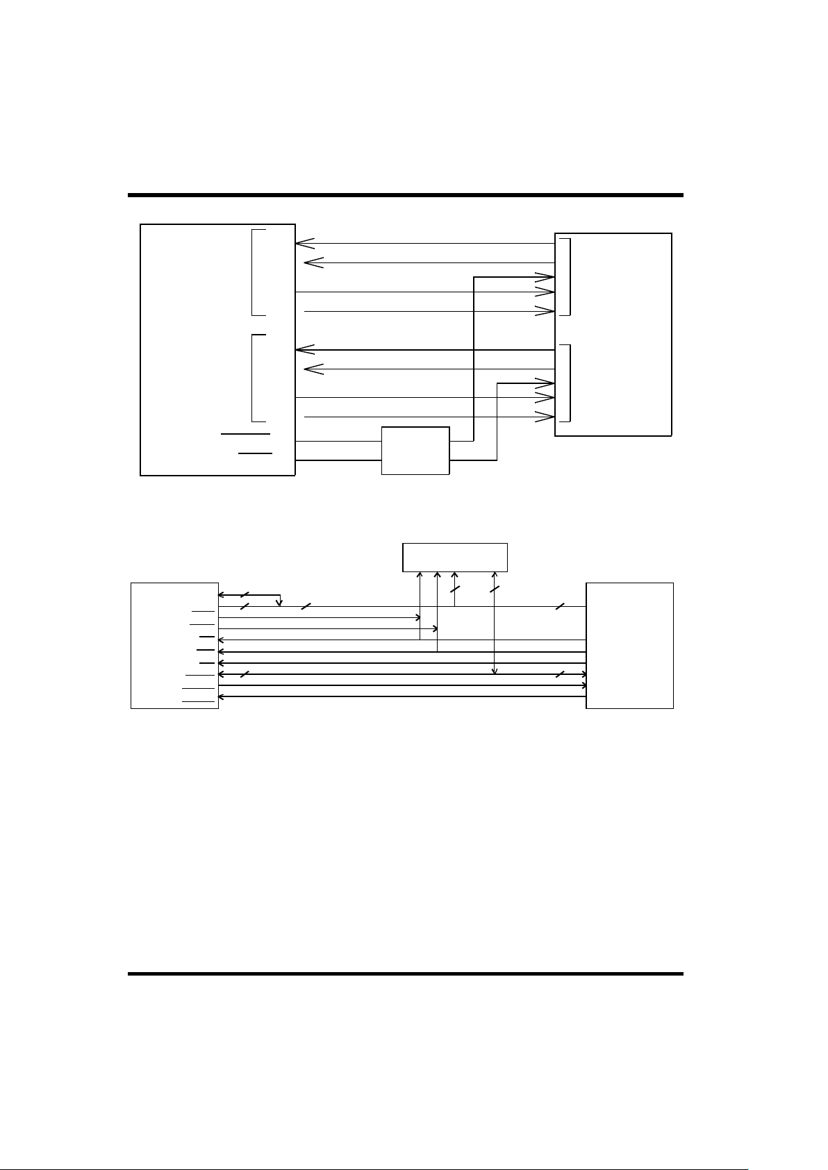
RTMP-30
CHANNEL
DISABLE
LOGIC
TXINHA
TXINHB
CHANNEL A
CHANNEL B
UTMC
RAO
RAZ
TAO
TAZ
RBO
RBZ
TBO
TBZ
CHANNEL A
CHANNEL B
RTMP
¤
¤
¤
¤
63M125
TIMERON
CHA/B
Figure 20. RTMP-to-Transceiver Interface Diagram
RAM
1616
16
16
HOST
16
16
13
3
RTMP
A3-A15
A0-A2
•
•
•
RRD
RWR
RD
WR
CS
DATA
DMAR
DMAG
Figure 21. RTMP-to Host Interface
Page 31

RTMP-31
7.0 OPERATING CONDITIONS*
(REFERENCED TO VSS)
SYMBOL PARAMETER LIMITS UNIT
DC supply voltage
Voltage on any pin
DC input current
Storage temperature
V
V
mA
Power dissipation
300 mW
Θ Thermal resistance, junction-to-case
10
Maximum junction temperature +175
V
DD
V
I/O
I
I
T
STG
P
D
T
J
±10
-0.3 to +7.0
-64 to +150
-0.3 to VDD +0.3
°C
°C/W
°C
* Stresses outside the listed absolute maximum ratings may cause permanent damage to the device. This is a stress rating only,
and functional operation of the device at these or any other conditions beyond limits indicated in the operational sections of
this specification is notrecommended. Exposure to absolute maximum rating conditions for extended periods may affect
device reliability.
RECOMMENDED OPERATING CONDITIONS
SYMBOL PARAMETER LIMITS UNIT
DC supply voltage
Temperature range
4.5 to 5.5 V
Operating frequency MHz
DC input voltage
V
V
DD
T
A
F
O
V
IN
12 ± .01%
0 to V
DD
-55 to +125
°C
Page 32

RTMP-32
8.0 DC ELECTRICAL CHARACTERISTICS
SYMBOL PARAMETER UNIT
Low-level input voltage
High-level input voltage
Input leakage current
Low-level output voltage
High-level output voltage
V
V
V
CONDITION MINIMUM MAXIMUM
TTL inputs
TTL inputs
TTL outputs
TTL outputs
Three-state output leakage
TTL outputs
current
0.8
2.0
TTL inputs
Inputs with pull-down resistors
Inputs with pull-up resistors
-1
100
-1000
1
1000
-100
µ
A
µ
A
µA
0.4 V
2.4
-10
µ
A
mA
20 pF
15 pF
10 pF
Notes:
5. Guaranteed by design or characterization.
2. Not more than one output may be shorted at a time for a maximum duration of one second.
Voltage supply should be adequately sized and decoupled to handle a large current surge.
50 mA
100 mA
3. Includes current through input pull-ups. Instantaneous surge currents on the order of 1 amp can occur during output switching .
+10
Inputs with pull-down resistors
400 µ
A
Quiescent current See Note 4 1 mA
4. All inputs with internal pull-ups and pull-downs should be left floating. All other inputs should be tied high or low.
-100
1. Measured only for initial qualification and after process or design changes which may affect input/output capacitance.
V
IL
V
IH
V
OL
V
OH
I
OZ
I
OS
I
DD
C
IN
C
OUT
C
IO
QI
DD
I
IN
V
IN
= VDD or V
SS
V
IN
= VDD
V
IN
= 2.4V
V
IN
= V
SS
I
OL
= 3.2mA
I
OH
= -400mA
VO = VDD or V
SS
V
DD
= 5.5V, VO = V
DD
V
DD
= 5.5V, VO = 0V
F = 1MHz @ 0V
F = 1MHz @ 0V
F = 1MHz @ 0V
F = 12MHz, CL = 50pF
Short-circuit output current
2, 5
Input capacitance
1
Output capacitance
1
Bidirect I/O capacitance
1
Average operating current
3, 5
Page 33

RTMP-33
9.0 AC ELECTRICAL CHARACTERISTICS
90%
Figure 23. AC Test Loads and Input Waveforms
Note:
50pF including scope probe and test socket
Input Pulses
10%10%
90%
< 2ns < 2ns
50pF
3V
0V
5V
•
I
REF
(source)
I
REF
(sink)
V
REF
to data valid
to high Z
to response
to response
to response
INPUT
INPUT
INPUT
INPUT
INPUT
INPUT
INPUT
to high Z
to data valid
to responseINPUT
PARAMETERSYMBOL
BUS
OUTPUT
OUT-OF-PHASE
OUTPUT
IN-PHASE
INPUT
Notes:
1. Timing measurements made at (VIH MIN + VIL MAX)/2.
2. Timing measurements made at (VOL MAX + VOH MIN)/2
3. Based on 50pF load.
4. Unless otherwise noted, all AC electrical characteristics are guaranteed by design or characterization.
1
1
2 2
2
2
V
IH
MIN
V
IH
MIN
V
OH
MIN
V
OH
MIN
V
OH
MIN
t
a
t
b
t
c
t
d
t
e
t
f
t
g
t
h
t
a
t
c
t
b
t
d
t
e
t
f
t
g
t
h
↑
↓
↓
↓
↓
↓
↓↑
↑
↑
↑
↑
Figure 22. Typical Timing Measurements
Page 34

RTMP-34
VALID AD-
SYMBOL PARAMETER UNITSMAXMIN
134 ns
ns
ns
ns
ns
ns
ns
ns
40 176
80 90
95 140
50
0
32 70
0 62
7.3
µ
s
BUS
DATA
BUS
ADDRESS
Note:
1. Guaranteed by test.
ns0
VALID
0
0
DMAR
DMAG
AV
RRD
t
22a
t
22b
(1)
t
22c
t
22d
t
22e
t
22f
t
22g
t
22a
t
22b
t
22c
t
22d
t
22e
t
22f
t
22g
t
22h
t
22i
t
22j
t
22h
t
22i
t
22j
DMAR ↓ to DMAG↓
AV ↑ to DMAG↑
Figure 24. Detailed Timing - RTMP DMA Read Cycle
DMAG↓ to Address Bus Valid
Address Bus Valid to AV↓
AV↓ to RRD↓
RRD Pulsewidth
Data Setup Time to RRD↑
Data Hold Time from RRD ↑
RRD ↑ to AV↑
AV↑ to Address High-Impedance (Hold) and DMAR↑
Page 35

RTMP-35
DMAG↓ to Address Bus Valid
Address Bus Valid to AV↓
AV↓ to RWR↓
RWR Pulsewidth
Data Setup Time to RWR↓
RWR↑ to Data Bus High-Impedance
RWR↑ to AV ↑
BUS
DATA
SYMBOL PARAMETER MIN MAX UNITS
0 93 ns
ns10 100
ADDRESS
BUS
DATA
BUS
SYMBOL PARAMETER UNITSMAXMIN
ns
ns
ns
ns
ns
ns
ns
ns
134
40 176
80 90
95 140
145 311
90
32 70
0 62
7.3 µs
Note:
1. Guaranteed by test.
ns0
VALID ADDRESS
VALID DATA
VALID DATA
BUS
VALID ADDRESS
20 ns
ns20
20
0
0
t
23a
t
23b
1
t
23c
t
23d
t
23e
t
23f
t
23g
t
23h
t
23i
t
23j
DMAR ↓ to DMAG↓
t
23a
t
23b
t
23c
t
23d
t
23f
t
23e
t
23g
t
23h
t
23i
t
23j
DMAR
DMAG
AV
RWR
CS*RD
t
24a
t
24b
1
t
24c
t
24d
Address Bus Valid to (CS*RD)↓
(CS*RD)↓ to Data Bus Valid
(CS*RD)↑ to Data Bus High-Impedence
(CS*RD)↑ to Address Bus High-Impedence
t
24a
t
24b
t
24c
t
24d
Figure 25. Detailed Timing - RTMP DMA Write Cycle
Figure 26. Detailed Timing X0106 RTMP Register Reads
Page 36

RTMP-36
1553
CMD WD
MCSA0-4
µ
3.7
240
230
240
SYMBOL PARAMETER UNITSMAXMIN
BUS
DATA
ADDRESS
SYMBOL MIN MAX UNITS
80
50
70
50
ns
ns
ns
ns
s
ns
100 ns
ns
ns
ILLCOM
BUS
ns20
SME
500 ns
1.0.100
µ
s
CS+WR
t
25
t
25
t
25
t
25
t
25
t
25
t
25
t
25
t
25
t
25
Address Bus Valid to (CS+WR)↓
PARAMETER
WR Pulsewidth
WR↑ to Data Bus High-Impedance (Hold time)
(CS*WR)↑ to Address Bus High-Impedance
Data Valid to (CS*WR)↑ (Set-up Time)
COMSTR
CHA/B
t
26
t26a
t
26
t26c
t26d
t26e
t26f
Mid-bit of Command Word Parity to COMSTRØ
COMSTR Pulsewidth
CHA/B Valid to COMSTR¦
MCSA0-4 Valid to COMSTR¦
COMSTR¦ to ILLCOM¦ (Active)
COMSTR¦ to SME¦ (Active)
SME
t26b
t
26
t
26
t
26
t
26
t
26
Figure 28. 1553 Command Strobeand Channel Timing
Figure 27. Detailed Timing - RTMP Register Writes
VALID DATA
VALID ADDRESS
Page 37

RTMP-37
10.09.25
5.754.25
1553B Mode Status Word Response Time
1553A Mode Status Word Response Time
CMD WD
1553
µ
SYMBOL PARAMETER UNITSMAXMIN
STATUS WORD
1553
Note:
1. This timing is for RTMP signals only and does not include delays from other sources.
s
µ s
t
RESP
(PRA/B=0)
t
RESP
(PRA/B=1)
t
RESP
1
Figure 29. 1553 Status Word Response Times
SWB14
SWB15
ADDRESS
TERMINALSYNC
WORD
STATUS
2
09876543210
1111111111987654321
TIMES
BIT
5 1 1 1 1 1 1 1 1 1 1 1 1
MESSAGE ERROR
SWB10
SWB11
SWB12
SWB13
SWB16
SWB17
SWB18
TFLG
PAR
Figure 30. Status Word Bit-Time Definitions for 1553A Mode
Page 38

RTMP-38
1 2 3 4 5 6 7 8 9 10 11 12 13 14 15 16 17 18 19 20
5 1 5 5 1
RESERVED
REMOTE TERMINAL
ADDRESS
SYNC
STATUS WORD
DATA WORD
SYNC
SYNC
DATA P
P
REMOTE TERMINAL
ADDRESS
T/R
SUBADDRESS/
MODE
DATA WORD
COUNT/MODE CODE
BIT TIMES
Note:
T/R - transmit/receive
P - parity
COMMAND WORD
INSTRUMENTATION
SERVICE REQUEST
BROADCAST COMMAND RECEIVED
BUSY
SUBSYSTEM FLAG
DYNAMIC BUS CONTROLACCEPTANCE
TERMINAL FLAG
PARITY
MESSAGE ERROR
Figure 31. MIL-STD-1553B Word Formats
Page 39

RTMP-39
SS
V
RTA4
TAPEN
A4
A0
A1
A2
A13
A14
A9
A8
A7
A10
A3
A11
A12
RAO
RESET
TBZ
TBO
TAO
RAZ
MCSA4
MCSA1
MCSA0
MCSA3
MCSA2
TEST
ENBC 73
72
71
70
69
68
67
66
65
64
63
62
61
60
59
58
57
56
55
54
535251504948474645444342414039383736353433
16
19
32
31
30
29
28
27
26
25
24
23
22
21
20
18
17
15
14
13
12 74 RTA3
RTPTY
11 10 9 8 7 6 5 4 3 2 1 84 83 82 81 80 79 78 77 76 75
SS
V
ILLCOM
DD
V
TAZ
DD
V
A5
A6
RBO
RBZ
CLK
EORT
EOMC
COMSTR
MERR
SVC
SME
CS
RD
WR
DMAR
DMAG
DMAEN
RRD
RWR
AV
A15
V
V
SS
DD
D0D1D2D3D4D5D6
D7D8D9
D10
D11
D12
D13
D14
D15
RTA0
RTA1
RTA2
V
V
SS
DD
CHA/B
TIMERON
MC/SA
PRA/B
Figure 32a. Leadless Chip Carrier Functional Pin Identification (Top View)
Page 40

RTMP-40
V
DD
BURST SSYSF
A
B
C
D
E
F
G
H
J
K
RBZ
CLK
MERR SME
DMAEN
D2
D3
D5
D6
D7D8
D9
D8 D11
D12
D13 D14
D15
RTA0
RTA1
A12A11
A3 A10
A7
A8
A15A9
A13
A2A1
A0
A4
RTPTY
L
ENBC
TEST MSCA2
MCSA3
MCSA0
MCSA1 MCSA4
TAOD1
TAZD0 TBO
TBZ RBO
RTA2 RTA4 A14
1110987654321
D4
INDEX
CORNER
RTA3 TAPEN
D10
RAO
A6
A5
ILLCOM
RAZ
TIMERON RESET
EORT
COMSTREOMC
SVC
CHA/B
PRA/B
MC/SA
V
SS
V
DD
V
DD
V
SS
V
DD
VDD VSS
DMAR
RDWRCS
DMAG
RRDAV
RWR
V
SS
Figure 32b. Pingrid Array Functional Pin Identification (Bottom View)
 Loading...