

Page 1
- May 1998
March 2001
USBN9603/USBN9604 Universal Serial Bus
Full Speed Node Controller with Enhanced DMA Support
USBN9603/USBN9604 Universal Serial Bus Full Speed Node Controller with Enhanced DMA Support
General Description
The USBN9603/4 are integrated, USB Node controllers.
Other than the reset mechanism for the clock generation circuit, these two devices are identical. All references to “the
device” in this document refer to both devices, unless otherwise noted.
The device provides enhanced DMA support with many automatic data handling features. It is compatible with USB
specification versions 1.0 and 1.1, and is an advanced version of the USBN9602.
The device integrates the required USB transceiver with a
3.3V regulator, a Serial Interface Engine (SIE), USB endpoint (EP) FIFOs, a versatile 8-bit parallel interface, a clock
generator and a MICROWIRE/PLUS™ interface. Seven
endpoint pipes are supported: one for the mandatory control endpoint and six to support interrupt, bulk and isochronous endpoints. Each endpoint pipe has a dedicated FIFO,
8 bytes for the control endpoint and 64 bytes for the other
endpoints. The 8-bit parallel interface supports multiplexed
and non-multiplexed style CPU address/data buses. A programmable interrupt output scheme allows device configuration for different interrupt signaling requirements.
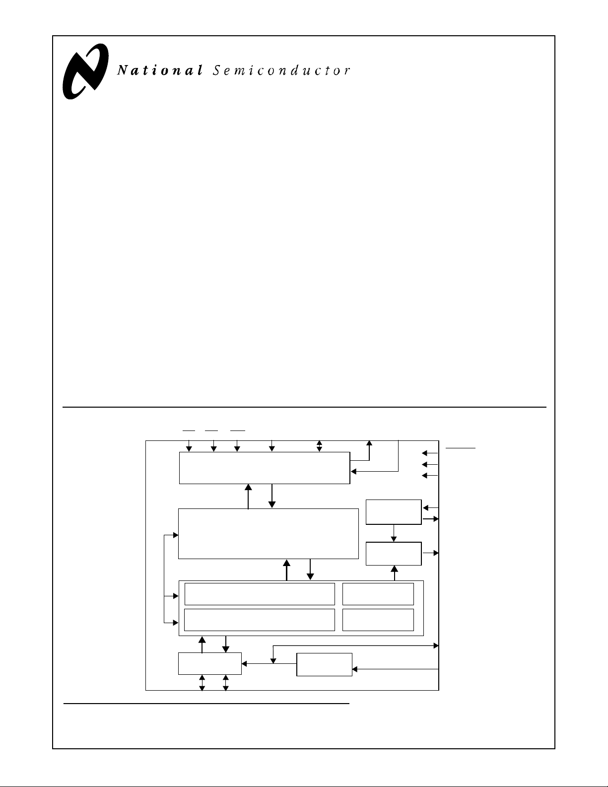
Block Diagram
CS RD WR
Microcontroller Interface
A0/ALE D7-0/AD7-0
Outstanding Features
●
Low EMI, low standby current, 24 MHz oscillator
●
Advanced DMA mechanism
●
Fully static HALT mode with asynchronous wake-up
for bus powered operation
●
5V or 3.3V operation
●
Improved input range 3.3V signal voltage regulator
●
All unidirectional FIFOs are 64 bytes
●
Power-up reset and startup delay counter simplify system design
●
Simple programming model controlled by external controller
●
Available in two packages
— USBN9603/4SLB: small footprint for new designs
and portable applications
— USBN9603/4-28M: standard package, pin-to-pin
compatible with USBN9602-28M
INTR
MODE1-0
RESET
V
CC
GND
24 MHz
Oscillator
XIN
XOUT
Endpoint/Control FIFOs
Clock
Generator
CLKOUT
Serial Interface Engine (SIE)
Media Access Controller (MAC)
Physical Layer Interface (PHY)
Clock
Recovery
USB Event
Detect
V3.3
Transceiver
D+ D-
National Semiconductor is a registered trademark of National Semiconductor Corporation. All other brand or product names are trademarks or registered
trademarks of their respective holders.
© National Semiconductor Corporation, 2001
Upstream Port
VReg
AGND
www.national.com
Page 2

Features
●
Full-speed USB node device
●
Integrated USB transceiver
●
Supports 24 MHz oscillator circuit with internal 48
MHz clock generation circuit
●
Programmable clock generator
●
Serial Interface Engine (SIE) consisting of Physical
Layer Interface (PHY) and Media Access Controller
(MAC), USB Specification 1.0 and 1.1 compliant
●
Control/Status register file
●
USB Function Controller with seven FIFO-based Endpoints:
— One bidirectional Control Endpoint 0 (8 bytes)
— Three Transmit Endpoints (64 bytes each)
— Three Receive Endpoints (64 bytes each)
●
8-bit parallel interface with two selectable modes:
— Non-multiplexed
— Multiplexed (Intel compatible)
●
Enhanced DMA support
— Automatic DMA (ADMA) mode for fully CPU-inde-
pendent transfer of large bulk or ISO packets
— DMA controller, together with the ADMA logic, can
transfer a large block of data in 64-byte packets via
the USB
— Automatic Data PID toggling/checking and NAK
packet recovery (maximum 256x64 bytes of data =
16K bytes)
●
MICROWIRE/PLUS interface
www.national.com
2
Page 3

Table of Contents
1.0 Signal/Pin Connection and Description
1.1 CONNECTION DIAGRAMS ........................................................................................................6
1.2 DETAILED SIGNAL/PIN DESCRIPTIONS ..................................................................................7
1.2.1 Power Supply ................................................................................................................ 7
1.2.2 Oscillator, Clock and Reset........................................................................................... 7
1.2.3 USB Port .......................................................................................................................8
1.2.4 Microprocessor Interface............................................................................................... 8
2.0 Functional Overview
2.1 TRANSCEIVER .........................................................................................................................10
2.2 VOLTAGE REGULATOR (VREG) .............................................................................................10
2.3 SERIAL INTERFACE ENGINE (SIE) .........................................................................................10
2.4 ENDPOINT PIPE CONTROLLER (EPC) ...................................................................................12
2.5 MICROCONTROLLER INTERFACE .........................................................................................12
3.0 Parallel Interface
3.1 NON-MULTIPLEXED MODE .....................................................................................................13
3.1.1 Standard Access Mode ...............................................................................................14
3.1.2 Burst Mode ..................................................................................................................14
3.1.3 User Registers .............................................................................................................14
3.2 MULTIPLEXED MODE ..............................................................................................................15
4.0 Direct Memory Access (DMA) Support
4.1 STANDARD DMA MODE (DMA) ...............................................................................................16
4.2 AUTOMATIC DMA MODE (ADMA) ...........................................................................................17
5.0 MICROWIRE/PLUS Interface
5.1 OPERATING COMMANDS .......................................................................................................19
5.2 READ AND WRITE TIMING ......................................................................................................20
6.0 Functional Description
6.1 FUNCTIONAL STATES .............................................................................................................22
6.1.1 Line Condition Detection .............................................................................................22
6.1.2 Functional State Transition ..........................................................................................22
6.2 ENDPOINT OPERATION ..........................................................................................................24
6.2.1 Address Detection .......................................................................................................24
6.2.2 Transmit and Receive Endpoint FIFOs .......................................................................24
6.2.3 Programming Model ....................................................................................................28
6.3 POWER SAVING MODES ........................................................................................................28
6.4 CLOCK GENERATION ..............................................................................................................29
7.0 Register Set
7.1 CONTROL REGISTERS ...........................................................................................................30
7.1.1 Main Control Register (MCNTRL) ............................................................................... 30
3
www.national.com
Page 4

Table of Contents (Continued)
7.1.2 Clock Configuration Register (CCONF)...................................................................... 31
7.1.3 Revision Identifier (RID) ..............................................................................................31
7.1.4 Node Functional State Register (NFSR) ..................................................................... 32
7.1.5 Main Event Register (MAEV) .......................................................................................32
7.1.6 Main Mask Register (MAMSK) ....................................................................................33
7.1.7 Alternate Event Register (ALTEV).............................................................................. 33
7.1.8 Alternate Mask Register (ALTMSK) ............................................................................34
7.1.9 Transmit Event Register (TXEV) .................................................................................34
7.1.10 Transmit Mask Register (TXMSK) ...............................................................................35
7.1.11 Receive Event Register (RXEV) ................................................................................. 35
7.1.12 Receive Mask Register (RXMSK) ...............................................................................35
7.1.13 NAK Event Register (NAKEV) .................................................................................... 36
7.1.14 NAK Mask Register (NAKMSK) ...................................................................................36
7.2 TRANSFER REGISTERS ..........................................................................................................36
7.2.1 FIFO Warning Event Register (FWEV) ....................................................................... 36
7.2.2 FIFO Warning Mask Register (FWMSK) .....................................................................37
7.2.3 Frame Number High Byte Register (FNH) .................................................................. 37
7.2.4 Frame Number Low Byte Register (FNL) ....................................................................37
7.2.5 Function Address Register (FAR) ................................................................................38
7.2.6 DMA Control Register (DMACNTRL).......................................................................... 38
7.2.7 DMA Event Register (DMAEV) ....................................................................................39
7.2.8 DMA Mask Register (DMAMSK) .................................................................................40
7.2.9 Mirror Register (MIR) ...................................................................................................41
7.2.10 DMA Count Register (DMACNT) .................................................................................41
7.2.11 DMA Error Register (DMAERR).................................................................................. 41
7.2.12 Wake-Up Register (WKUP) ........................................................................................ 42
7.2.13 Endpoint Control 0 Register (EPC0) ............................................................................43
7.2.14 Transmit Status 0 Register (TXS0) ............................................................................. 43
7.2.15 Transmit Command 0 Register (TXC0) ..................................................................... 44
7.2.16 Transmit Data 0 Register (TXD0) ................................................................................44
7.2.17 Receive Status 0 Register (RXS0) ..............................................................................44
7.2.18 Receive Command 0 Register (RXC0) ....................................................................... 45
7.2.19 Receive Data 0 Register (RXD0) ................................................................................ 45
7.2.20 Endpoint Control X Register (EPC1 to EPC6) .............................................................46
7.2.21 Transmit Status X Register (TXS1, TXS2, TXS3) .......................................................46
7.2.22 Transmit Command X Register (TXC1, TXC2, TXC3) ................................................47
7.2.23 Transmit Data X Register (TXD1, TXD2, TXD3) .........................................................48
7.2.24 Receive Status X Register (RXS1, RXS2, RXS3) .......................................................48
7.2.25 Receive Command X Register (RXC1, RXC2, RXC3) ................................................49
7.2.26 Receive Data X Register (RXD1, RXD2, RXD3) .........................................................50
4
www.national.com
Page 5

Table of Contents (Continued)
7.3 REGISTER MAP ........................................................................................................................50
8.0 Device Characteristics
8.1 ABSOLUTE MAXIMUM RATINGS ............................................................................................52
8.2 DC ELECTRICAL CHARACTERISTICS ...................................................................................52
8.3 AC ELECTRICAL CHARACTERISTICS ....................................................................................53
8.4 PARALLEL INTERFACE TIMING (MODE1-0 = 00B) ................................................................54
8.5 PARALLEL INTERFACE TIMING (MODE1-0 = 01B) ................................................................55
8.6 DMA SUPPORT TIMING ...........................................................................................................57
8.7 MICROWIRE INTERFACE TIMING (MODE1-0 = 10B) .............................................................58
8.8 RESET TIMING) ........................................................................................................................58
www.national.com
5
Page 6
1.0 Signal/Pin Connection and Description
1.1 CONNECTION DIAGRAMS
D2
D1
D0/SO
A0/ALE/SI
27
28
26
25
24
DACK
DRQ
23
INTR
22
D3
D4
D5
D6
D7
RESET
AGND
1
2
3
4
5
6
7
CS
RD
WR/SK
INTR
DRQ
DACK
A0/ALE/SI
D0/SO
D1
D2
D3
D4
D5
D6
28-Pin CSP
9
8
V3.3
10
D+
USBN9603/4SLB
1
2
3
4
5
6
7
28-Pin SO
8
9
10
11
12
13
14
21
WR/SK
20
RD
CS
19
CLKOUT
18
XOUT
17
XIN
16
MODEO
15
11
12
13
14
GND
V
CC
GND
D−
MODE1
28
CLKOUT
27
XOUT
26
XIN
MODE0
25
MODE1
24
GND
23
22
Vcc
21
GND
20
D–
19
D+
V3.3
18
17
AGND
RESET
16
D7
15
www.national.com
USBN9603/4-28M
6
Page 7

1.0 Signal/Pin Connection and Description (Continued)
1.2 DETAILED SIGNAL/PIN DESCRIPTIONS
1.2.1 Power Supply I/O Name Description
NA Vcc Digital Power Supply (V
level as GND and then raised to the required V
to be set to their reset values, the clock generator to be reset and stalls the CLKOUT output for
14
2
XIN clock cycles. During this time, no internal register is accessible.
NA GND Digital Power Supply (GND)
NA AGND Analog Power Supply (AGND)
). Power-on reset is detected when the input voltage is at the same
CC
level. The power-on reset causes all registers
cc
NA V3.3 Transceiver 3.3V Voltage Supply. This pin can be used as the internal 3.3V voltage regulator
output. The regulator is intended to power onlythe internal transceiver and one external pull-up.
An external 1 µF de-coupling capacitor is requiredon this pin. The voltage regulator output is disabled upon reset. When the internal voltageregulator is left disabled, this pin must be used as a
3.3V supply input for the internal transceiver. This is the case during 3.3V operation.
1.2.2 Oscillator, Clock and Reset I/O Name Description
NA XIN Crystal Oscillator Input. Input for internal 24 MHz crystal oscillator circuit. A 24 MHz funda-
mental crystal may be used.
NA XOUT Crystal Oscillator Output
O CLKOUT Clock Output. This programmable clock output may be disabled and configured for different
speeds via the Clock Configuration register. After a power-on reset and hardware reset (assertion of
In the USBN9604, a hardware reset causes CLKOUT to stall for 2
RESET), a4 MHz clock signal is output (there may be an initial phase discontinuity).
14
XIN clock cycles while the
internal DLL is synchronized to the external reference clock.
I RESET Reset. Activelow, assertion of RESETindicates a hardware reset, which causes all registers
in the device to revert to their reset values.
In the USBN9604, the hardware reset action is identical to a power-on reset. Signal conditioning is provided on this input to allow use of a simple, RC power-on reset circuit.
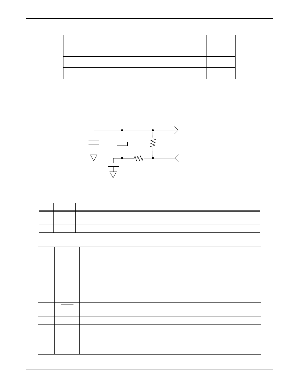
Oscillator Circuit
The XIN and XOUT pins may be connected to make a 24 MHz closed-loop, crystal-controlled oscillator. Alternately, an external 24 MHz clock source may be used as the input clock for the device. The internal crystal oscillator uses a 24 MHz
fundamental crystal. See Table 1 for typical component values and Figure 1 for the crystal circuit. For a specific crystal,
please consult the manufacturer for recommended component values.
If an external clock source is used, it is connected to XIN. XOUT should remain unconnected.Stray capacitance and inductance should be kept as low as possible in the oscillator circuit. Trace lengths should be minimized by positioning the crystal
and external components as close as possible to the XIN and XOUT pins.
Table 1. Approximate Component Values
Component Parameters Values Tolerance
Crystal Resonator Resonance Frequency 24 MHz 2500 ppm
Type AT-Cut
(max)
Maximum Serial Resistance 50 Ω
Maximum Shunt Capacitance 10 pF
Load Capacitance 20 pF
Resistor R1
1MΩ±5%
7
www.national.com
Page 8
1.0 Signal/Pin Connection and Description (Continued)
Component Parameters Values Tolerance
Resistor R2
Capacitor C1
Capacitor C2
0 ΝΑ
15 pF ±20%
15 pF ±20%
External Elements
Choose C1 and C2 capacitors (see Figure 1) to match the crystal’s load capacitance. The load capacitance C
the crystal is comprised of C1 in series with C2, and in parallel with the parasitic capacitance of the circuit. The parasitic
“seen” by
L
capacitance is caused by the chip package, board layout and socket (if any), and can vary from 0 to 8 pF. The rule of thumb
in choosing these capacitors is:
= (C1*C2)/(C1+C2)+C Parasitic
C
L
XIN
XTAL
C1
R1
XOUT
C2
R2
Figure 1. Typical Oscillator Circuit
1.2.3 USB Port I/O Name Description
I/O D+ USB D+ Upstream Port. This pin requires an external 1.5k pull-up to 3.3V to signal fullspeed
operation.
I/O D– USB D– Upstream Port
1.2.4 Microprocessor Interface I/O Name Description
I MODE1-0 Interface Mode. Each of these pins should be hard-wired to V
or GND to select the inter-
CC
face mode:
MODE1-0 = 00. Mode 0: Non-multiplexed parallel interface mode
MODE1-0 = 01. Mode 1: Multiplexed parallel interface mode
MODE1-0 = 10. Mode 2: MICROWIRE interface mode
MODE1-0 = 11. Mode 3: Reserved
Note: Mode 3 also selects the MICROWIRE interface mode in the USBN9602, but this mode
should be reserved to preserve compatibility with future devices.
I
DACK DMAAcknowledge. This activelow signalis onlyused ifDMA isenabled. IfDMA isnot used,
this pin must be tied to V
CC
.
O DRQ DMA Request. This pin is used for DMA request only if DMA is enabled.
O INTR Interrupt. The interrupt signal modes (active high, active low or open drain) can be config-
ured via the Main Control register. During reset, this signal is TRI-STATE.
I
I
www.national.com
CS Chip Select. Active low chip select
RD Read. Active low read strobe, parallel interface
8
Page 9

1.0 Signal/Pin Connection and Description (Continued)
I WR Write. Active low write strobe, parallel interface
SK MICROWIRE Shift Clock. Mode 2
IA0A0 Address Bus Line. Mode 0, parallel interface
ALE Address Latch Enable. Mode 1, parallel interface
SI MICROWIRE Serial Input. Mode 2
I/O D0 Data Bus Line D0. Mode 0
AD0 Address/Data Bus LIne AD0. Mode 1
SO MICROWIRE Serial Output. Mode 2
I/O D1 Data Bus Line D1. Mode 0
AD1 Address/Data Bus Line AD1. Mode 1
I/O D2 Data Bus Line D2. Mode 0
AD2 Address/Data Bus Line AD2. Mode 1
I/O D3 Data Bus Line D3. Mode 0
AD3 Address/Data Bus Line AD3. Mode 1
I/O D4 Data Bus Line D4. Mode 0
AD4 Address/Data Bus Line AD4. Mode 1
I/O D5 Data Bus Line D5. Mode 0
AD5 Address/Data Bus Line AD5. Mode 1
I/O D6 Data Bus Line D6. Mode 0
AD6 Address/Data Bus Line AD6. Mode 1
I/O D7 Data Bus Line D7. Mode 0
AD7 Address/Data Bus Line AD7. Mode 1
9
www.national.com
Page 10

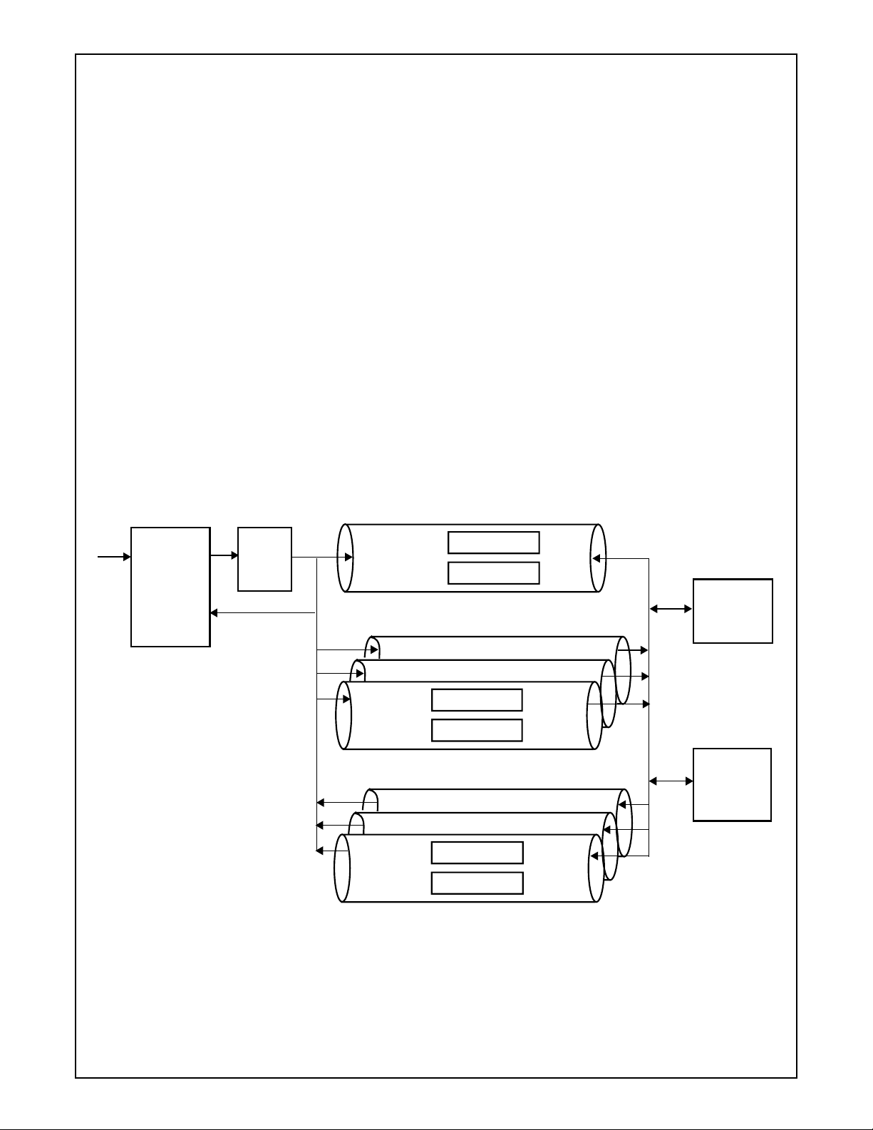
2.0 Functional Overview
The device is a Universal Serial Bus (USB) Node controller compatible with USB Specification, 1.0 and 1.1. It integrates onto
a single IC the required USB transceiver with a 3.3V regulator, the Serial Interface Engine (SIE), USB endpoint FIFOs, a
versatile (8-bit parallel or serial) interface and a clock generator. A total of seven endpoint pipes are supported: one bidirectional for the mandatory control EP0 and an additional six for unidirectional endpoints to support USB interrupt, bulk and
isochronous data transfers. The 8-bit parallel interface supports multiplexed and non-multiplexed style CPU address/data
buses. The synchronous serial MICROWIRE interface allows adapting to CPUs without external address/data buses. A programmable interrupt output scheme allows adapting to different interrupt signaling requirements.
Refer to Figure 2 for the major functional blocks, described in the following sections.
2.1 TRANSCEIVER
The device contains a high-speed transceiver which consists of three main functional blocks:
— Differential receiver
— Single-ended receiver with on-chip voltage reference
— Transmitter with on-chip current source.
This transceiver meets the performance requirements described in Chapter 7 of the USB Specification, Version 1.1.
To minimize signal skew, the differential outputswings of thetransmitter are well balanced. Slew-rate control is used on the
driver to minimize radiated noise and crosstalk. The drivers support TRI-STATE operationto allow bidirectional,half-duplex
operation of the transceiver.
The differential receiver operates over the complete common mode range, and has a delay guaranteed to be larger than
that of the single-ended receivers. This avoids potential glitches in the Serial Interface Engine (SIE) after single-ended zeros.
Single-ended receivers are present on each of the two datalines. These are required, in addition to the differential receiver, to
detect an absolute voltage with a switching threshold between 0.8V and 2.0V (TTL inputs). To increase V
glitching, a voltage reference sets the single-ended switchingreference. An external 1.5± 5% KΩ resistor isrequired on D+ to
indicate that this is a high-speed node. This resistor should be tied to a voltage source between 3.0V and 3.6V, and referenced
to the local ground, such as the output provided on pin V3.3.
rejection, without
cc
2.2 VOLTAGE REGULATOR (VREG)
The voltage regulator provides 3.3V for the integrated transceiver from 5.0V device power or USB bus power. This output
can be used to supply power to the 1.5 KΩ pull-up resistor. This output must be decoupled with a 1 µF tantalum capacitor
to ground. It can be disabled under software control to allow using the device in a 3.3V system.
2.3 SERIAL INTERFACE ENGINE (SIE)
The SIE is comprised of physical (PHY) and Media Access Controller (MAC) modules. The PHY module includes the digitalclock recovery circuit, a digital glitch filter, End Of Packet (EOP) detection circuitry, and bit stuffing and unstuffing logic. The
MAC module includes packet formatting, CRC generation and checking, and endpoint address detection. It provides the
necessary control to give the NAK, ACK and STALL responses as determined by the Endpoint Pipe Controller (EPC) for the
specified endpoint pipe. The SIE is also responsible for detecting and reporting USB-specific events, such as NodeReset,
NodeSuspend and NodeResume. The module output signals to the transceiver are well matched (under 1 nS) to minimize
skew on the USB signals.
The USB specifications assign bit stuffing and unstuffing as the method to ensure adequate electrical transitions on the line
to enable clock recovery at the receiving end. The bit stuffing block ensures that whenever a string of consecutive 1’s is
encountered, a 0 is inserted after every sixth 1 in the data stream. The bit unstuffing logic reverses this process.
The clock recovery block uses the incoming NRZI data to extract a data clock (12 MHz) from a 48 MHz input clock. This
input clock is derived from a 24 MHz oscillator in conjunction with PLL circuitry (clock doubler). This clock is used in the data
recovery circuit. The output of this block is binary data (decoded from the NRZI stream) which can be appropriately sampled
using the extracted 12 MHz clock. The jitter performance and timing characteristics meet the requirements set forth in Chapter 7 of the USB Specification.
www.national.com
10
Page 11
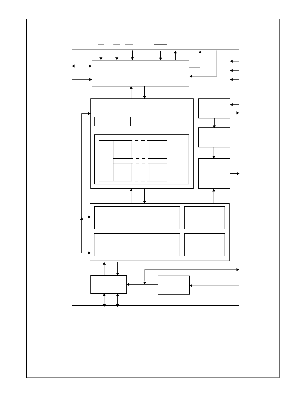
2.0 Functional Overview (Continued)
D7-0/AD7-0/SO
A0/ALE/SI
CS RD WR/SK
Microcontroller Interface
(Parallel and Serial)
Endpoint/Control FIFOs
EP2
Endpoint0
EP1
DACK
EP6EP5
StatusControl
DRQ
RX
TX
INTR
MODE1-0
24 MHz
Oscillator
PLL
x 2
Clock
Generator
RESET
V
CC
GND
XIN
XOUT
CLKOUT
SIE
Media Access Controller (MAC)
Physical Layer Interface (PHY)
Transceiver
D+ D-
Upstream Port
Figure 2. USBN9603/4 Block Diagram
VReg
Clock
Recovery
USB Event
Detect
V3.3
AGND
11
www.national.com
Page 12
2.0 Functional Overview (Continued)
2.4 ENDPOINT PIPE CONTROLLER (EPC)
The EPC provides the interface for USB function endpoints. An endpoint is the ultimate source or sink of data. An endpoint
pipe facilitates the movement of data between USB and memory, and completes the path between the USB host and the
function endpoint. According to the USB specification, up to 31 such endpoints are supported at any given time. USB allows
a total of 16 unidirectional endpoints for receive and 16 for transmit. As the control endpoint 0 is always bidirectional, the
total number is 31. Seven endpoint pipes with the same function address are supported. See Figure 3 for a schematic diagram of EPC operation.
A USB function is a USB device that is able to transmit and receive information on the bus. A function may have one or more
configurations, each of which defines the interfaces that make up the device. Each interface, in turn, is composed of one or
more endpoints.
Each endpoint is an addressable entity on USB and is required to respond to IN and OUT tokens from the USBhost (typically
a PC). IN tokens indicate that the host has requested toreceive information from an endpoint,and OUT tokens indicatethat
it is about to send information to an endpoint.
On detection of an IN token addressed to an endpoint, the endpoint pipe should respond with a data packet. If the endpoint
pipe is currently stalled, a STALL handshake packet is sent under software control. If the endpoint pipe is enabled but no
data is present, a NAK (Negative Acknowledgment) handshake packet is sent automatically. If the endpoint pipe is isochronous and enabled but no data is present, a bit stuff error followed by an end of packet is sent on the bus.
Similarly, on detection of an OUT token addressed to an endpoint, the endpoint pipe should receive a data packet sent by
the host and load it into the appropriate FIFO. If the endpoint pipe is stalled, a STALL handshake packet is sent. If the endpoint pipe is enabled but no buffer is present for data storage, a NAK handshake packet is sent. If the endpoint is isochronous and enabled but cannot handle the data, no handshake packet is sent.
A disabled endpoint does not respond to IN, OUT, or SETUP tokens.
The EPC maintains separate status and control information for each endpoint pipe.
For IN tokens, the EPC transfers data from the associated FIFO to the host. For OUT tokens, the EPC transfers data in the
opposite direction.
USB
USB SIE
Function
Address
Compare
EP0
EPB
EPC.
EPY
EPZ
Control Registers
FIFOs
Control Endpoint Pipe
EPA
Control Registers
FIFO
Receive Endpoint Pipes
EPX
Control Registers
FIFO
Transmit Endpoint Pipes
DMA
Controller
Microcontroller
Interface
Figure 3. EPC Operation
2.5 MICROCONTROLLER INTERFACE
The device can be connected to a CPU or microcontroller via the 8-bit parallel or MICROWIRE interface. The interface type
is selected by the input mode pins MODE0 and MODE1. In addition, a configurable interrupt output is provided. The interrupt
type can be configured to be either open-drain active-low or push-pull active high or low.
www.national.com
12
Page 13
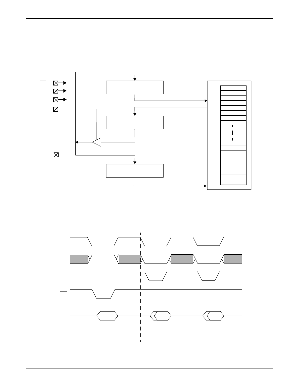
3.0 Parallel Interface
The parallel interface allows the device to function as a CPU or microcontroller peripheral. This interface type and its addressing mode (multiplexed or non-multiplexed) is determined via device input pins MODE0 and MODE1.
3.1 NON-MULTIPLEXED MODE
Non-multiplexed mode uses the control pins
in Figure 4. This mode is selected by tying both the MODE1 and MODE0 pins to GND.
CS, RD, WR, the address pin A0 andthe bidirectional data bus D7-0 as shown
CS
A0
WR
RD
D7-0
Figure 4. Non-Multiplexed Mode Block Diagram
The CPU has direct access to the DATA_IN, DATA_OUT and ADDR registers. Reading and writing data to the device can
be done either in standard access or burst mode. See Figure 5 for timing information.
DATA_IN
DATA_OUT
ADDR
0x00
Data In
Data Out
Address
0x3F
Register File
CS
A0
RD
WR
D7-0
OutInput
Write Address
Figure 5. Non-Multiplexed Mode Timing Diagram
Read Data Burst Read Data
13
Out
www.national.com
Page 14

3.0 Parallel Interface (Continued)
3.1.1 Standard Access Mode
The standard access sequence for non-multiplexed mode is to write the address to the ADDR register and then read or write
the data from/to the DATA_OUT/DATA_IN register. The DATA_OUT register is updated after writing to the ADDR register.
The ADDR register or the DATA_OUT/DATA_IN register is selected with the A0 input.
3.1.2 Burst Mode
In burst mode, the ADDR register is written once with the desired memory address of any of the on-chip registers. Then
consecutive reads/writes are performed to the DATA_IN/DATA_OUT register without previously writing a new address. The
content of the DATA_OUT register for read operations is updated once after every read or write.
3.1.3 User Registers
The following table gives an overview of the parallel interface registers in non-multiplexed mode.
The reserved bits return undefined data on read and should be written with 0.
A0 Access bit 7 bit 6 bit 5 bit 4 bit 3 bit 2 bit 1 bit 0
0 Read DATA_OUT
0 Write DATA_IN
1 Read Reserved
1 Write Reserved ADDR5-0
Address Register (ADDR)
The ADDR register acts as a pointer to the internal memory. This register is write only and is cleared on reset.
Data Output Register (DATA_OUT)
The DATA_OUT register is updated with the contents of the memory register to which the ADDR register is pointing. Update
occurs under the following conditions:
1. After the ADDR register is written.
2. After a read from the DATA_OUT register.
3. After a write to the DATA_IN register.
This register is read only and holds undefined data after reset.
Data Input Register (DATA_IN)
The DATA_IN register holds the data written to the device address to which ADDR points. This register is write only and is
cleared on reset.
14
www.national.com
Page 15
3.0 Parallel Interface (Continued)
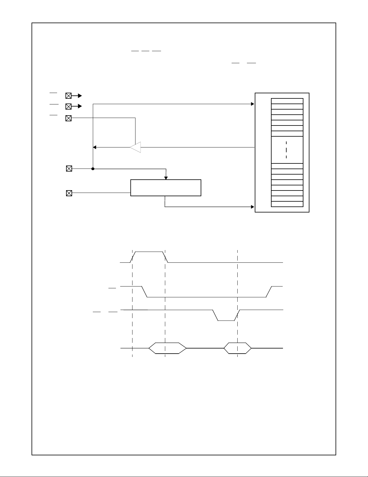
3.2 MULTIPLEXED MODE
Multiplexed mode uses the control pins
bus AD7-0 as shown in Figure 6. This mode is selected by tying MODE1 to GND andMODE0 to V
into the ADDR register when ALE is high. Data is output/input with the next active
accessible in this interface mode.
Figure 7 shows basic timing of the interface in Multiplexed mode.
CS, RD, WR, the address latch enable signal ALE and the bidirectional address data
RD or WR signal. All registers are directly
. The address is latched
CC
CS
WR
RD
AD7-0
ALE
ALE
Data Out
EN
ADDR
Address
Figure 6. Multiplexed Mode Block Diagram
Data In
0x00
0x3F
Register File
www.national.com
CS
RD or WR
AD7-0
ADDR
DATA
Figure 7. Multiplexed Mode Basic Read/Write Timing
15
Page 16

4.0 Direct Memory Access (DMA) Support
The device supports DMA transfers with an external DMA controller from/to endpoints 1 to 6. This mode uses the device
pins DRQ and
with parallel interface mode (MODE1 must be grounded). The read or write address is generated internally and the state of
the A0/ALE pin is ignored during a DMA cycle.
The DMA support logic has a lower priority than the parallel interface.
comes active,
given time to issue a DMA request when data is received or transmitted.
Two different DMA modes are supported: standard and automatic.
4.1 STANDARD DMA MODE (DMA)
To enable DMA transfers in standard DMA mode, the following steps must be performed:
1. The local CPU programs the DMA controller for fly-by demand mode transfers. In this mode, transfers occur only when
the device requests them via the DRQ pin. The data is read/written from/to the device receive/transmit FIFO and written/read into/from local memory during the same bus transaction.
2. TheDMA address counter is programmed to point to the destination memory block in the local shared memory, and the
Byte Count register is programmed with the number of bytes in the block to be transferred. If required the automatic error
handling should be enabled at this point along with the error handling counter. In addition the user needs to set the respective Endpoint enable bit.
3. The DMA Enable bit and DMA Source bits are set in the DMACNTRL register.
4. The USB host can now perform USB bulk or isochronous data transfers over the USB bus to the receive FIFO or from
the transmit FIFO in the device.
5. Ifthe FIFOs warning limit is reached or the transmission/reception is completed, a DMA request/acknowledge sequence
is initiated for the predetermined number of bytes. The time at which a DMA request is issued depends on the selected
DMA mode (controlled by the DMOD bit in the DMACNTRL register), the current status of the endpoint FIFO, and the
FIFO warning enable bits. A DMA request can be issued immediately.
6. After the DMA controller has granted control of the bus, it drives a valid memory address and asserts
WR, thus transferring a byte from the receive FIFO to memory, or from memory tothe transmit FIFO. This process continues until the DMA byte count, within the DMA controller, reaches zero.
7. Afterthe programmed amount of data is transferred, thefirmware must do one of the following (depending on the transfer
direction and mode):
— Queue the new data for transmission by setting the TX_EN bit in the TXCx register.
— Set the End Of Packet marker by setting the TX_LAST bit in the TXCx register. Re-enable reception by setting the
RX_EN bit in the RXCx register.
— Check if the last byte of the packet was received (RX_LAST bit in the RXSx register).
The DMA transfer can be halted at any time by resetting the DMA Request Enable bit. If the DMA Request Enable bit is
cleared during the middle of a DMA cycle, the current cycle is completed before the DMA request is terminated.
See Figures 8 and 9 for the transmit and receive sequences using standard DMA mode.
DACK in addition to the parallel interface pins RD or WR and D7-0 data pins. DMA mode can only be used
CS must stay inactive during a DMA cycle. If CS be-
DACK is ignored and a regular read/write operation is performed. Only one endpoint can be enabled at any
DACK and RD or
www.national.com
MIcrocontroller
Set up DMA
Figure 8. Transmit Operation in Standard DMA Mode
Microcontroller
Set up DMA
Transaction
Read FIFO
16
USB
DMA
DMA
Fill FIFO
Microcontroller
Enable RX
DMA
Fill FIFO
Microcontroller
Enable RX
Figure 9. Receive Operation in Standard DMA Mode
Microcontroller
Enable TX
USB
Transaction
time
time
Page 17

4.0 Direct Memory Access (DMA) Support (Continued)
4.2 AUTOMATIC DMA MODE (ADMA)
The ADMA mode allows the CPU to transfer independently large bulk or isochronous data streams to or from the USB bus.
The application’s DMA controller, together with the ADMA logic, have the capability to split a large amount of data and transfer it in (FIFO size) packets via the USB. In addition, automatic error handling is performed in order to minimize firmware
intervention. The number of transferred data stream bytes must be of a modulo 64 size. The maximum amount of data is
restricted to 256*64 bytes = 16 Kbytes.
To enable an ADMA transfer, the following steps must be performed:
1. The local CPU programs the DMA controller for fly-by demand mode transfers. In this mode, transfers occur only in response to DMA request via the DRQ pin. The data is read/written from/to the receive/transmit FIFO and written/read into/from local memory during the same bus transaction.
2. TheDMA address counter is programmed to point to the destination memory block in the local shared memory, and the
Byte Count register is programmed with the number of bytes in the block to be transferred. The DMA Count register must
be configured with the number of packets to be received or transmitted. If required, the Automatic Error Handling register
must also be configured at this time.
3. The ADMA enable bit must be set prior to, or at the same time as the DMA enable bit. The DMA enable bit must be
cleared before enabling ADMA mode.
4. The DMA Request Enable bit and DMA Source bits are set in the device.The respective endpoint Enable bit must also
be set.
5. The USB host can now perform USB bulk or isochronous data transfers over the USB bus to the receive FIFO or from
the transmit FIFO. Steps 5 to 7 of the normal DMA mode are perfromed automatically. The ADMA is stopped either when
the last packet is received or when the DMA Count register has reached the value zero.
See Figures 10 and 11 for the transmit and receive sequences using ADMA mode. See Figures 12 and 13 for the basic
DMA write timing and read timing.
Microcontroller
Set up ADMA
Microcontroller
Set up ADMA
DMA
Fill FIFO
Figure 10. Transmit Operation Using ADMA Mode
USB
Transaction
Figure 11. Receive Operation Using ADMA Mode
USB
Transaction
DMA
Read FIFO
DMA
Fill FIFO
USB
Transaction
USB
Transaction
DMA
Read FIFO
USB
Last
Transaction
DMA
Last
Read FIFO
time
time
17
www.national.com
Page 18
4.0 Direct Memory Access (DMA) Support (Continued)
DRQ
DACK
WR
D7-0
DRQ
DACK
RD
D7-0
Input
Figure 12. DMA Write to USBN9603/4
Output
Figure 13. DMA Read from USBN9603/4
www.national.com
18
Page 19

5.0 MICROWIRE/PLUS Interface
The MICROWIRE/PLUS interface allows the device to function asa CPU or microcontrollerperipheral via a serial interface.
This mode is selected by pulling the MODE1 pin high and the MODE0 pin low.The MICROWIRE/PLUS mode uses the chip
select (
CS), serial clock (SK), serial data in (SI) and serial data out (SO) pins, as shown in Figure 14.
0x00
Data Out
SK
CS
SYNC
DATA_OUT
SO
SHIFT
SI
Data In
DATA_IN
ADDR
Address
CMD1-0
0x3F
Register File
Figure 14. MICROWIRE/PLUS Interface Block Diagram
5.1 OPERATING COMMANDS
The MICROWIRE/PLUS interface is enabled by a falling edge of
CS and reset with a rising edge of CS. Data on SI is shifted
in after the rising edge of SK. Data is shifted out on SO after the falling edge of SK. Data is transferred from/to the Shift
register after the falling edge of the eighth SK clock. Data is transferred with the most significant bit first. Table 2 summarizes
the available commands (CMD) for the MICROWIRE/PLUS interface.
Note: A write operation to any register always reads the contents of the register after the write has occurred, and shifts out
that data in the next cycle. This read does not clear the bit in the respective registers, even for a Clear on Read (CoR) type
bit, with one exception: writing to the TXDx (transmit data) registers, which causes undefined data to be read during the next
cycle.
Table 2. Command/Address Byte Format
Byte Transferred
Sequence Initiated
1
CMD ADDR
Cycle Description
10543210
0 0 RADDR
(read)
12Shift in CMD/RADDR; shift out previous read data
Shift in next CMD/ADDR; shift out RADDR data
0 1 x 1 no action; shift out previous read data (do not clear CoR bits)
1 0 WADDR
(normal write)
12Shift in CMD/WADDR; shift out previous read data
Shift in WADDR write data; shift out WADDR read data (do
not clear CoR bits)
1 1 WADDR
(burst write)
1
Shift in CMD/WADDR; shift out previous read data
2-n
Shift in WADDR write data; shift out WADDR read data (do
not clear CoR bits); terminate this mode by pulling
CS high
1. 1 cycle = 8 SK clocks. Data is transferred after the 8th SK of 1 cycle.
19
www.national.com
Page 20

5.0 MICROWIRE/PLUS Interface (Continued)
5.2 READ AND WRITE TIMING
Data is read by shifting in the 2-bit command (CMD and the 6-bit address, RADDR or WADDR) while simultaneously shifting
out read data from the previous address.
Data can be written in standard or burst mode. Standard mode requires two bytes: one byte for the command and address
to be shifted in, and one byte for data to be shifted in. In burst mode, the command and address are transferred first, and
then consecutive data is written to that address. Burst mode is terminated when
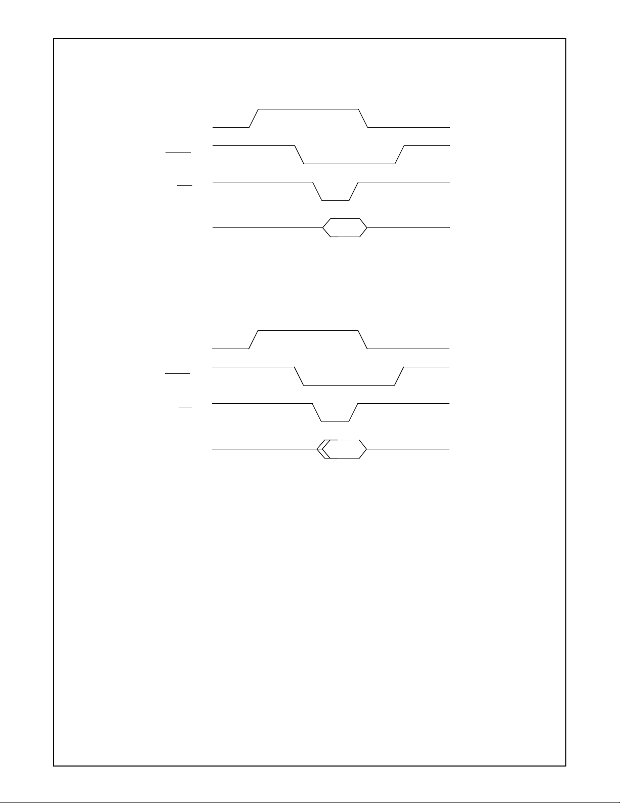
See Figure 15 for basic read timing, Figure 16 for standard write timing, and Figure 17 for write timing in burst mode.
CS
CS becomes inactive (high).
SK
SI
SO
CS
SK
8 Cycles
CMD = 0x ADDR CMD = 0x ADDR New Command
Undefined Data Read Data Read Data
Figure 15. Basic Read Timing
8 Cycles
8 Cycles 8 Cycles
8 Cycles 8 Cycles
SI
SO
CMD = 10 ADDR Write Data New Command
Undefined Data Read Data Read Data
Figure 16. Standard Write Timing
20
www.national.com
Page 21

5.0 MICROWIRE/PLUS Interface (Continued)
CS
SK
SI
SO
8 Cycles
CMD=11 ADDR Write Data Write Data
Undefined Data Read Data Read Data
Figure 17. Burst Write Timing
8 Cycles 8 Cycles
www.national.com
21
Page 22

6.0 Functional Description
6.1 FUNCTIONAL STATES
6.1.1 Line Condition Detection
At any given time, the device is in one of the following states (see Section 6.1.2 for the functional state transitions):
• NodeOperational Normal operation
• NodeSuspend Device operation suspended due to USB inactivity
• NodeResume Device wake-up from suspended state
• NodeReset Device reset
The NodeSuspend, NodeResume, or NodeReset line condition causes a transition from one operating state to another.
These conditions are detected by specialized hardware and reported via the Alternate Event (ALTEV) register. If interrupts
are enabled, an interrupt is generated upon the occurrence of any of the specified conditions.
NodeOperational
This is the normal operating state of the device. In this state, the node is configured for operation on the USB bus.
NodeSuspend
A USB device is expected to enter NodeSuspend state when 3 mS have elapsed without any detectable bus activity. The
device looks for this event and signals itby setting the SD3 bit in the ALTEV register, which causesan interrupt, if enabled,
to be generated. The firmware should respond by putting the device into the NodeSuspend state.
IThe device can resume normal operation under firmware control in response to a local event at the host controller. It can
wake up the USB bus via a NodeResume, or when detecting a resume command on the USB bus, which signals an interrupt
to the host controller.
NodeResume
If the host has enabled remote wake-ups from the node, the device can initiate a remote wake-up.
Once the firmware detects the event, which wakes up the bus, it releases the device from NodeSuspend state by initiating
a NodeResume on the USB using the NFSR register. The node firmware must ensure at least 5 mS of Idle on the USB.
While in NodeResume state, a constant “K” is signalled on the USB. This should last for at least 1 mS and no more than 5
mS, after which the USB host should continue sending the NodeResume signal for at least an additional 20 mS, and then
completes the NodeResume operation by issuing the End Of Packet (EOP) sequence.
To successfully detect the EOP, the firmware must enter USB NodeOperational state by setting the NFSR register.
If no EOP is received from the host within 100 mS, the software must reinitiate NodeResume.
NodeReset
When detecting a NodeResume or NodeReset signal while in NodeSuspend state, the device can signal this to the main
controller by generating an interrupt.
USB specifications require that a device must be ready to respond to USB tokens within 10 mS after wake-up or reset.
6.1.2 Functional State Transition
Figure 18 shows the device states and transitions, as well as the conditions that trigger each transition. All state transitions
are initiated by the firmware.
www.national.com
22
Page 23

6.0 Functional Description (Continued)
NodeOperational
suspend_det &
set_suspend
resume_det &
NodeSuspend
11b
set_oper
10b
local_event & sd5_detect &
clear_suspend
reset_det &
resume_compl &
set_oper
NodeResume
01b
set_oper
set_reset
reset_det &
hw/swreset
NodeReset
00b
set_reset
Bold Italics
Notes:
1. When the node is not in NodeOperational state, all registers are frozen with the exception of the endpoint controller state machines, and the TX_EN, LAST and RX_EN bits which are reset.
1. In NodeResume state, resume signaling is propagated upstream.
2. In NodeSuspend state, the node may enter a low power state and is able to detect resume signaling.
Figure 18. Node Functional State Diagram
Table 3. Functional States
State
Transition
set_reset
set_suspend
set_oper
clear_suspend
Node Functional State register NFS[1:0] bits are written with 00
The firmware should only initiate set_reset if RESET in the ALTEV register is set.
Node Functional State register NFS[1:0] bits are written with 11
The firmware should only initiate set_suspend if SD3 in the ALTEV register is set.
Node Functional State register NFS[1:0] bits are written with 10
Node Functional State register NFS[1:0] bits are written with 01
The firmware should only initiate clear_suspend if SD5 in the ALTEV register is set.
Condition Asserted
reset_det RESET in the ALTEV register is set to 1
=
Transition initiated by firmware
b
b
b
b
local_event A local event that should wake up the USB.
sd5_det SD5 in the ALTEV register is set to 1.
suspend_det SD3 in the ALTEV register is set to 1.
resume_det RESUME in the ALTEV register is set to1.
The node should stay in NodeResume state for at least 10mS and then must enter
resume_compl
USB Operational state to detect the EOP from the host, which terminates this Remote
Resume operation. EOP is signalled when EOP in the ALTEV register is set to 1.
23
www.national.com
Page 24

6.0 Functional Description (Continued)
6.2 ENDPOINT OPERATION
6.2.1 Address Detection
Packets are broadcast from the host controller to all the nodes on the USB network. Address detection is implemented in
hardware to allow selective reception of packets and to permit optimal use of microcontroller bandwidth. One function address with seven different endpoint combinations is decoded in parallel. If a match is found, then that particular packet is
received into the FIFO; otherwise it is ignored.
The incoming USB Packet Address field and Endpoint field are extracted from the incoming bitstream. Then the address
field is compared to the Function Address register (FADR). If a match is detected, the Endpoint field is compared to all of
the Endpoint Control registers (EPCx) in parallel.A match then causes the payload data to be received or transmitted using
the respective endpoint FIFO.
ADDR Field Endpoint Field
FADR Register
match
EPC0 Register
EPC1 Register
EPC2 Register
EPC3 Register
EPC4 Register
EPC5 Register
- USB Packet -
match
Receive/Transmit FIFO0
Transmit FIFO1
Receive FIFO1
Transmit FIFO2
Receive FIFO2
Transmit FIFO3
Receive FIFO3
EPC6 Register
Figure 19. USB Function Address/Endpoint Decoding
6.2.2 Transmit and Receive Endpoint FIFOs
The device uses a total of seventransmit and receive FIFOs: one bidirectional transmit and receive FIFO for the mandatory
control endpoint, three transmit FIFOs and three receive FIFOs. As shown in Table 4, the bidirectional FIFO for the control
endpoint is 8 bytes deep. The additional unidirectional FIFOs are 64 bytes each for both transmit and receive. Each FIFO
can be programmed for one exclusive USB endpoint, used together with one globally decoded USB function address. The
firmware must not enable both transmit and receive FIFOs for endpoint zero at any given time.
www.national.com
24
Page 25

6.0 Functional Description (Continued)
Table 4. USBN9603/4 Endpoint FIFO Sizes
TX FIFO RX FIFO
Endpoint No.
Size (Bytes) Name Size (Bytes) Name
0 8 FIFO0
1 64 TXFIFO1
2 64 RXFIFO1
3 64 TXFIFO2
4 64 RXFIFO2
5 64 TXFIFO3
6 64 RXFIFO3
If two endpoints in the same direction are programmed with the same endpoint number and both are enabled, data is received or transmitted to/from the endpoint with the lower number, until that endpoint is disabled for bulk or interrupt transfers,
or becomes full or empty for ISO transfers. For example, if receive EP2 and receive EP4 both use endpoint 5 and are both
isochronous, the first OUT packet is received into EP2 and the second OUT packet into EP4, assuming no firmware interaction inbetween. For ISO endpoints, this allows implementing a ping-pong buffer scheme together with the frame number
match logic.
Endpoints in different directions programmed with the same endpoint number operate independently.
Bidirectional Control Endpoint FIFO0 Operation
FIFO0 should be used for the bidirectional control endpoint zero. It can be configured to receive data sent to the default
address with the DEF bit in the EPC0 register. Isochronous transfers are not supported for the control endpoint.
The Endpoint 0 FIFO can hold a single receive or transmit packet with up to 8 bytes of data. Figure 20 shows the basic
operation in both receive and transmit direction.
Note: The actual current operating state is not directly visible to the user.
FLUSH Bit, RXC0 Register
RX_EN Bit, RXC0 Register
RXWAIT
SETUP Token
OUT or
SETUP Token
FIFO0 Empty
(All Data Read)
Write to TXD0
TXFILL
TX_EN Bit,
TXC0 Register (*)
TXWAIT
IN token
FLUSH Bit TXC0 Register
IDLE
Transmission
Done
TX
(*) For zero length packet, TX_EN causes a transition from IDLE to TXWAIT
Figure 20. Endpoint 0 Operation
25
RX
www.national.com
Page 26

6.0 Functional Description (Continued)
A packet written to the FIFO is transmitted if an IN token for the respective endpoint is received. If an error condition is detected, the packet data remains in the FIFO and transmission is retried with the next IN token.
The FIFO contents can be flushed to allow response to an OUT token or to write new data into the FIFO for the next IN token.
If an OUT token is received for the FIFO, the firmware isinformed that the FIFO has received dataonly if there wasno error
condition (CRC or STUFF error). Erroneous receptions are automatically discarded.
Transmit Endpoint FIFO Operation (TXFIFO1, TXFIFO2, TXFIFO3)
The Transmit FIFOs for Endpoints 1, 3 and 5 support bulk, interrupt and isochronous USB packet transfers larger than the
actual FIFO size. Therefore. the firmware must update the FIFO contents while the USB packet is transmitted on the bus.
Figure 21 illustrates the operation of the transmit FIFOs.
FLUSH (Resets TXRP and TXWP)
TXRP
TFxS - 1
0x0
+
TXFL = TXWP - TXRP
+
Tx FIFO X
TXWP
+
TCOUNT = TXRP - TXWP (= TFxS - TXFL)
Figure 21. Tx FIFO Operation
TFxS
Transmit FIFO x Size. This is the total number of bytes available within the FIFO.
TXRP
Transmit Read Pointer. This pointer is incremented every time the Endpoint Controller reads from the transmit FIFO. This
pointer wraps around to zero if TFxS is reached. TXRP is never incremented beyond the value of the write pointer TXWP.
An underrun condition occurs if TXRP equals TXWP and an attempt is made to transmit more bytes when the LAST bit in
the TXCMDx register is not set.
TXWP
Transmit Write Pointer. This pointer is incremented every time the firmware writes to the transmit FIFO. This pointer wraps
around to zero if TFxS is reached.
If an attempt is made to write more bytes to the FIFO than actual space available (FIFO overrun), the write to the FIFO is
ignored. If so, TCOUNT is checked for an indication of the number of empty bytes remaining.
TXFL
Transmit FIFO Level. This value indicates how many bytes are currently in the FIFO.
A FIFO warning is issued if TXFL decreases to a specific value. The respective WARNx bit in the FWR register is set if TXFL
is equal to or less than the number specified by the TFWL bit in the TXCx register.
www.national.com
26
Page 27

6.0 Functional Description (Continued)
TCOUNT
Transmit FIFO Count. This value indicates how many empty bytes can be filled within the transmit FIFO. This value is accessible by firmware via the TxSx register.
Receive Endpoint FIFO Operation (RXFIFO1, RXFIFO2, RXFIFO3)
The Receive FIFOs for the Endpoints 2, 4 and 6 support bulk, interrupt and isochronous USB packet transfers larger than
the actual FIFO size. If the packet length exceeds the FIFO size, the firmware must read the FIFO contents while the USB
packet is being received on the bus. Figure 22 shows the detailed behavior of receive FIFOs.
FLUSH (Resets RXRP and RXWP)
RXRP
RFxS - 1
0x0
RCOUNT = RXWP - RXRP
+
+
Rx FIFO X
RXWP
+
RXFL = RXRP - RXWP (= RFxS - RCOUNT)
Figure 22. Rx FIFO Operation
RFxS
Receive FIFO x Size. This is the total number of bytes available within the FIFO.
RXRP
Receive Read Pointer. This pointer is incremented with every read of the firmware from the receive FIFO. This pointer wraps
around to zero if RFxS is reached. RXRP is never incremented beyond the value of RXWP.
If an attempt is made to read more bytes than are actually available (FIFO underrun), the last byte is read repeatedly.
RXWP
Receive Write Pointer. This pointer is incremented every time the Endpoint Controller writes to the receive FIFO.This pointer
wraps around to zero if RFxS is reached.
An overrun condition occurs if RXRP equals RXWP and an attempt is made to write an additional byte.
RXFL
Receive FIFO Level. This value indicates how many more bytes can be received until an overrun condition occurs with the
next write to the FIFO.
A FIFO warning is issued if RXFL decreases to a specific value. The respective WARNx bit in the FWR register is set if RXFL
is equal to or less than the number specified by the RFWL bit in the RXCx register.
RCOUNT
Receive FIFO Count. This value indicates how many bytes can be read from the receive FIFO. This value is accessible by
firmware via the RXSx register.
27
www.national.com
Page 28

6.0 Functional Description (Continued)
6.2.3 Programming Model
Figure 23 illustrates the register hierarchy for event reporting.
.
MAEV
FWEV
TXEVRXEV
NAKEVALTEV
TXS0
TXC0
TXD0
EPC0
RXS0
RXC0
FIFO0
8 byte
RXD0
TXSx
TXCx
EPCx
TFIFOx
64 byte
TXDx
RXSy
RXCx
EPCy
RFIFOy
64 byte
RXDy
Figure 23. Register Hierarchy
6.3 POWER SAVING MODES
To minimize the power consumption of the USB node, the device can be set to a static Halt mode. During Halt mode, the
clock oscillator circuit is disabled, stopping the external 24 MHz clock and 48 MHz frequency doubler, as well as the clock
output signal provided on the CLKOUT pin. However, all device internal status and register settings are preserved.
The device is set to Halt mode under the following conditions:
●
If Halt On Suspend (HOS) is enabled (the HOS bit in the WKUP register is set to 1), the device enters Halt mode
when the node is set in Suspend state. Writing a 1 to HOS after the node is in Suspend state has no effect.
●
If the node is not attached, the device enters Halt mode, when the Force Halt bit (FHT) in the Wake-Up register is
set to 1.
www.national.com
28
Page 29

6.0 Functional Description (Continued)
Power-On Reset
External RESET
14
2
cycles
Power-Up
Delay
Power-Up Delay
Wake-Up
Timeout
Event
Halt
Active
Halt On Suspend
or Force Halt
Figure 24. Power Saving Modes
The device exits Halt mode in response to one of the following wake-up events:
●
A high-to-low transition is detected on the CS pin and the wake-up Enable bit, ENUC in the WKUP register, is set to
1.
●
Any activity on the USB is detected (USB not idle) and the wake-up Enable bit, ENUSB in the WKUP register is set
to 1. (The node can detect any USB activity only when it is attached.)
14
When a valid wake-up event is detected, the device returns to active mode after a power-up delay of 2
XIN clock cycles
has elapsed (approximately 680 usec ). This delay is established by a 14-bit delay counter, which ensures that the 24 MHz
oscillator has reached a stable condition and the clock doubler locks and generates a stable 48 MHz signal. After this startup delay, the clock signal can be output on the CLKOUT pin.
6.4 CLOCK GENERATION
The Clock Generator provides the CLKOUT output signal based on the programming of the Clock Configuration register
(CCONF). This allows disabling of the output clock and selection of a clock divisor. The clock divisor supports a programmable output in the range of 48 MHz to 2.82 MHz. On a power-on reset, the output clock defaults to 4 MHz. A software reset
has no effect on the programming of the CCONF, and thus no effect on the CLKOUT signal.
The only difference between the USBN9603 and USBN9604 devices is the effect of a hardware reset on the clock generation circuit. In the USBN9604, assertion of the
RESET input causes the clock generation circuit to be reset, whereas in the
USBN9603, the clock generation circuit is not reset.
In the USBN9603, however, assertion of the
RESET input does cause all registers to revert to their reset values, including
CCONF, which then forces the CLKOUT signal to its default of 4 MHz.
In the USBN9604, assertion of the
As part of the clock generation reset, a delay of 2
sertion of the
RESET input also causes all registers to revert to their reset values, including CCONF, which then forces the
RESET input causes the clock generation circuit to be reset as with the power-on reset.
14
XIN clock cycles is incurred before the CLKOUT signal is output. As-
CLKOUT signal to its default of 4 MHz.
This difference is particularly important for bus-powered operations. In such applications, the voltage provided by the bus
may fall below acceptable levels for the clock generation circuit. When this occurs, a reset must be applied to this circuit to
guarantee proper operation. After a delay of 2
14
XIN clock cycles, the CLKOUT signal is output. This low voltage detection
is typically accomplished in bus-powered applications using a voltage sensor, such as the LP3470, to appropriately reset
the CPU and other components, including the USBN9604.
In self-powered applications where there is direct control over the voltage supply, there is no need for the
cause the clock generation circuitry to be reset and the CLKOUT signal to stall for 2
14
XIN clock cycles. The USBN9603 is
RESET input to
thus suited for self-powered applications that use the CLKOUT signal as a system clock.
29
www.national.com
Page 30

7.0 Register Set
The device has a set of memory-mapped registers that can be read from/writtento control the USB interface. Someregister
bits are reserved; reading from these bits returns undefined data. Reserved register bits should always be written with 0.
The following conventions are used to describe the register format:
Bit Number bit 7 bit 6 bit 5 bit 4 bit 3 bit 2 bit 1 bit 0
Bit Mnemonic Abbreviated bit/field names
Corresponding FIFO Corresponding FIFO types and numbers, where relevant
Reset Value reset values, where relevant
r = Read only
w = Write only
Register Type
7.1 CONTROL REGISTERS
7.1.1 Main Control Register (MCNTRL)
bit 7 bit 6 bit 5 bit 4 bit 3 bit 2 bit 1 bit 0
INTOC1-0 Reserved NAT VGE Reserved SRST
r/w = Read and write by firmware
CoR = Cleared on read
CoW = Cleared on write if written with 0; writing a 1 has no effect
HW = Modified by the device and by firmware
00-00 0
r/w - r/w r/w r/w
SRST
Software Reset. Setting this bit causes a software reset of the device. This reset is equivalent to a hardware reset except
that the Clock Configuration (CCONF) register is unaffected. All registers revert to their default values. This bit is cleared
automatically upon completion of the initiated reset.
VGE
Voltage Regulator Enable. Setting this bit enables the internal 3.3V voltage regulator. This bit is hardware reset only to a 0,
disabling the internal 3.3V regulator by default. When the internal 3.3V regulator is disabled, the device is effectively disconnected from USB. Upon power-up, the firmware may perform any needed initialization (such as power-on self test) and then
set the VGE bit. Until the VGE bit is set, the upstream hub port does not detect the device presence.
If the VGE bit is reset an external 3.3V power supply may be used on the V3.3 pin.
NAT
Node Attached. This bit indicates that this node is ready to be detected as attached to USB. When reset the transceiver
forces SE0 on the USB port to prevent the hub (to which this node is connected to) from detecting an attach event. After
reset, this bit is left cleared to give the device time before it must respond to commands. After this bit is set, the device no
longer drives the USB and should be ready to receive Reset signaling from the hub.
The NAT bit should be set by the firmware if an external 3.3V supply has been provided to the V3.3 pin, or at least 1 mS
after the VGE bit is set (in the latter case, the delay allows the internal regulator sufficient time to stabilize).
INTOC
Interrupt Output Control. These bits control interrupt ouput according to the following table.
www.national.com
30
Page 31

7.0 Register Set (Continued)
Table 5. Interrupt Output Control Bits
INTOC
Interrupt Output
10
0 0 Disabled
0 1 Active low open drain
1 0 Active high push-pull
1 1 Active low push-pull
7.1.2 Clock Configuration Register (CCONF)
bit 7 bit 6 bit 5 bit 4 bit 3 bit 2 bit 1 bit 0
CODIS Reserved CLKDIV3-0
0-1011
r/w - r/w
CLKDIV
External Clock Divisor. The power-on reset and a hardware reset configure the divisor to 11
a 4 MHz output clock.
frequency = 48 MHz / (CLKDIV+1)
If the CLKDIV value is changed by firmware, the clock output is expanded/shortened if the CLKDIV value is increased/decreased in its current phase, to allow glitch-free switching at the CLKOUT pin.
(decimal format), which yields
d
CODIS
Clock Output Disable. Setting this bit disables the clock output. The CLKOUT output signal is frozen in its current state and
resumes with a new period when this bit is cleared.
7.1.3 Revision Identifier (RID)
This register holds the binary encoded chip revision.
bit 7 bit 6 bit 5 bit 4 bit 3 bit 2 bit 1 bit 0
Reserved REVID3-0
-0010
-r
REVID
Revision Identification. For revision 9603 Rev A and 9604 Rev A, the field contains 0010
.
b
31
www.national.com
Page 32

7.0 Register Set (Continued)
7.1.4 Node Functional State Register (NFSR)
bit 7 bit 6 bit 5 bit 4 bit 3 bit 2 bit 1 bit 0
Reserved NFS1-0
-00
- r/w
NFS
Node Functional State. The firmware should initiate all required state transitions according to the respective status bits in
the Alternate Event (ALTEV) register. The valid transitions are shown in Figure 18. The node functional state bits set the
node state, as shown in Table 6.
Table 6. USB Functional States
NFS
Node State Description
10
0 0 NodeReset This is the USB Reset state. This is entered upon a module
0 1 NodeResume In this state, resume "K" signalling is generated. This state
1 0 NodeOperational This is the normal operational state. In this state the node is
1 1 NodeSuspend Suspend state should be entered by firmware on detection of a
7.1.5 Main Event Register (MAEV)
bit 7 bit 6 bit 5 bit 4 bit 3 bit 2 bit 1 bit 0
reset or by software upon detection of a USB Reset. Upon entry,
all endpoint pipes are disabled. DEF in the Endpoint Control 0
(EPC0) register and AD_EN in the Function Address (FAR)
register should be cleared by software on entry to this state. On
exit, DEF should be reset so the device responds to the default
address.
should be entered by firmware to initiate a remote wake-up
sequence by the device. The node must remain in this state for
at least 1 mS and no more than 15 mS.
configured for operation on the USB bus.
Suspend event while in Operational state. While in Suspend
state, the transceivers operate in their low-power suspend mode.
All endpoint controllers and the bits TX_EN, LAST and RX_EN
are reset, while all other internal states are frozen. On detection
of bus activity, the RESUME bit in the ALTEV register is set. In
response, software can cause entry to NodeOperational state.
INTR RX_EV ULD NAK FRAME TX_EV ALT WARN
00 000 000
see text r CoR r CoR r r r
WARN
One of the unmasked bits in the FIFO Warning Event (FWEV) register has been set. This bit is cleared by reading the FWEV
register.
ALT
Alternate. One of the unmasked ALTEV register bits has been set. This bit is cleared by reading the ALTEV register.
www.national.com
32
Page 33

7.0 Register Set (Continued)
TX_EV
Transmit Event. This bit is set if any of the unmasked bits in the Transmit Event (TXEV) register (TXFIFOx or TXUNDRNx)
is set. Therefore, it indicates that an IN transaction has been completed. This bit is cleared when all the TX_DONE bits and
the TXUNDRN bits in each Transmit Status (TXSx) register are cleared.
FRAME
This bit is set if the frame counter is updated with a new value. This can be due to receipt of a valid SOF packet on the USB
or to an artificial update if the frame counter was unlocked or a frame was missed. This bit is cleared when the register is
read.
NAK
Negative Acknowledge. One of the unmasked NAK Event (NAKEV) register bits has been set. This bit is cleared when the
NAKEV register is read.
ULD
Unlock Locked Detected. The frame timer has either entered unlocked condition from a locked condition, or has re-entered
a locked condition from an unlocked condition as determined by the UL bit in the Frame Number (FNH or FNL) register that
is set. This bit is cleared when the register is read.
RX_EV
Receive Event. This bit is set if any of the unmasked bits in the Receive Event (RXEV) register is set. It indicates that a
SETUP or OUT transaction has been completed. This bit is cleared when all of the RX_LAST bits in each Receive Status
(RXSx) register and all RXOVRRN bits in the RXEV register are cleared.
INTR
Master Interrupt Enable. This bit is hardwired to 0 in the Main Event (MAEV) register; the corresponding bit in the Main Mask
(MAMSK) register is the Master Interrupt Enable.
7.1.6 Main Mask Register (MAMSK)
When set to 1, an interrupt is enabled when the respective event in the MAEV register is enabled. Otherwise, interrupt generation is disabled.
bit 7 bit 6 bit 5 bit 4 bit 3 bit 2 bit 1 bit 0
Same Bit Definition as MAEV Register
00000000
r/w
7.1.7 Alternate Event Register (ALTEV)
bit 7 bit 6 bit 5 bit 4 bit 3 bit 2 bit 1 bit 0
RESUME RESET SD5 SD3 EOP DMA WKUP res
0000000-
CoR CoR CoR CoR CoR r r -
WKUP
Wake-Up Event. This bit is set when a wake-up interrupt is generated and issued on the external INTR pin. The WKUP bit
is read only and cleared when the corresponding wake-up pending bit (PNDUC and/or PNDUSB in the Wake-Up (WKUP)
register) is cleared.
DMA
DMA Event. One of the unmasked bits in the DMA Event (DMAEV) register has been set. The DMA bit is read only and
cleared when the DMAEV register is cleared.
33
www.national.com
Page 34

7.0 Register Set (Continued)
EOP
End of Packet. A valid EOP sequence was detected on the USB. It is used when this device has initiated a Remote wake-up
sequence to indicate that the Resume sequence has been acknowledged and completed by the host. This bit is cleared when
the register is read.
SD3
Suspend Detect 3 mS. This bit is set after 3 mS of IDLE is detected on the upstream port, indicating that the device should
be suspended. The suspend occurs under firmware control by writing the suspend value to the Node Functional State (NFSR) register. This bit is cleared when the register is read.
SD5
Suspend Detect 5 mS. This bit is set after 5 mS of IDLE is detected on the upstream port, indicating that this device is permitted to perform a remote wake-up operation. The resume may be initiated under firmware control by writing the resume
value to the NFSR register. This bit is cleared when the register is read.
RESET
This bit is set when 2.5 µS of SEO is detected on the upstream port. In response, the functional state should be reset (NFS
in the NFSR register is set to RESET), where it must remain for at least 100 µS. The functional state can then return to Operational state. This bit is cleared when the register is read.
RESUME
Resume signalling is detected on USB when the device is in Suspendstate (NFS in the NFSRregister is set to SUSPEND),
and a non IDLE signal is present on USB, indicating that this device should begin its wake-up sequence and enter Operational state. This bit is cleared when the register is read.
7.1.8 Alternate Mask Register (ALTMSK)
A bit set to 1 in this register enables automatic setting of the ALT bit in the MAEV register when the respective event in the
ALTEV register occurs. Otherwise, setting ALT bit is disabled.
bit 7 bit 6 bit 5 bit 4 bit 3 bit 2 bit 1 bit 0
Same Bit Definition as ALTEV Register
0 0 0 0 000 -
r/w -
7.1.9 Transmit Event Register (TXEV)
bit 7 bit 6 bit 5 bit 4 bit 3 bit 2 bit 1 bit 0
TXFIFO3 TXFIFO2 TXFIFO1 FIFO0 TXFIFO3 TXFIFO2 TXFIFO1 FIFO0
TXUDRRN3-0 TXFIFO3-0
0000 0 0 00
r
1
r
1. Since Endpoint 0 implements a store and forward principle, an underrun condition for
FIFO0 cannot occur. This results in the TXUDRRN0 bit always being read as 0.
TXFIFO
Transmit FIFO. These bits are a copy of the TX_DONE bits from the corresponding Transmit Status (TXSx) registers. The
bits are set when the IN transaction for the corresponding transmit endpoint is complete. The bits are cleared when the corresponding TXSx register is read.
TXUDRRN
Transmit Underrun. These bits are copies of the respective TX_URUN bits from the corresponding TXSx registers. Whenever any of the Transmit FIFOs underflow, the respective TXUDRRN bit is set. These bits are cleared when the corresponding Transmit Status register is read.
www.national.com
34
Page 35

7.0 Register Set (Continued)
7.1.10 Transmit Mask Register (TXMSK)
When set and the corresponding bit in the TXEV register is set, TX_EV in the MAEV register is set. When cleared, the corresponding bit in the TXEV register does not cause TX_EV to be set.
bit 7 bit 6 bit 5 bit 4 bit 3 bit 2 bit 1 bit 0
Same Bit Definition as TXEV Register
00000000
r/w
7.1.11 Receive Event Register (RXEV)
bit 7 bit 6 bit 5 bit 4 bit 3 bit 2 bit 1 bit 0
RXFIFO3 RXFIFO2 RXFIFO1 FIFO0 RXFIFO3 RXFIFO2 RXFIFO1 FIFO0
RXOVRRN3-0 RXFIFO3-0
00000000
CoR r
RXFIFO
Receive FIFO. These bits are set whenever either RX_ERR or RX_LAST in the respective Receive Status (RXSx) register
is set. Reading the corresponding RXSx register automatically clears these bits.
The device discards all packets for Endpoint 0 received with errors. This is necessary in case of retransmission due to media
errors, ensuring that a good copy of a SETUP packet is captured. Otherwise, the FIFO may potentially be tied up, holding
corrupted data and unable to receive a retransmission of the same packet (the RXFIFO0 bit does only reflect the value of
RX_LAST for Endpoint 0).
If data streaming is used for the receive endpoints (EP2, EP4 and EP6) the firmware must check with the respective
RX_ERR bits to ensure the packets received are not corrupted by errors.
RXOVRRN
Receive Overrun. These bits are set in the event of a FIFO overrun condition. They are cleared when the register is read.
The firmware must check with the respective RX_ERR bits that packets received for the other receive endpoints (EP2, EP4
and EP6) are not corrupted by errors, as these endpoints support data streaming (packets which are longer than the actual
FIFO depth).
7.1.12 Receive Mask Register (RXMSK)
When set and the corresponding bit in the RXEV register is set, RX_EV in the MAEV register is set. When cleared, the corresponding bit in the RXEV register does not cause RX_EV to be set.
bit 7 bit 6 bit 5 bit 4 bit 3 bit 2 bit 1 bit 0
Same Bit Definition as RXEV Register
00000000
r/w
35
www.national.com
Page 36

7.0 Register Set (Continued)
7.1.13 NAK Event Register (NAKEV)
bit 7 bit 6 bit 5 bit 4 bit 3 bit 2 bit 1 bit 0
RXFIFO3 RXFIFO2 RXFIFO1 FIFO0 TXFIFO3 TXFIFO2 TXFIFO1 FIFO0
OUT3-0 IN3-0
00000000
CoR CoR
IN
Set to 1 when a NAK handshake is generated for an enabled address/endpoint combination (AD_EN in the Function Address, FAR, register is set to 1 and EP_EN in the Endpoint Control, EPCx, register is set to 1) in response to an IN token.
This bit is cleared when the register is read.
OUT
Set to 1 when a NAK handshake is generated for an enabled address/endpoint combination (AD_EN in the FAR register is
set to 1 and EP_EN in the EPCx register is set to 1) in response to an OUT token. This bit is not set if NAK is generated as
result of an overrun condition. It is cleared when the register is read.
7.1.14 NAK Mask Register (NAKMSK)
When set and the corresponding bit in the NAKEV register is set, the NAK bit in the MAEVregister is set. When cleared, the
corresponding bit in the NAKEV register does not cause NAK to be set.
bit 7 bit 6 bit 5 bit 4 bit 3 bit 2 bit 1 bit 0
Same Bit Definition as NAKEV Register
00000000
r/w
7.2 TRANSFER REGISTERS
7.2.1 FIFO Warning Event Register (FWEV)
bit 7 bit 6 bit 5 bit 4 bit 3 bit 2 bit 1 bit 0
RXFIFO3 RXFIFO2 RXFIFO1 - TXFIFO3 TXFIFO2 TXFIFO1 -
RXWARN3-1 Reserved TXWARN3-1 Reserved
000-000-
rr-
TXWARN
Transmit Warning. Set to 1 when the respective transmit endpoint FIFO reaches the warning limit, as specified by the TFWL
bits of the respective TXCx register, and transmission from the respective endpoint is enabled. This bit is cleared when the
warning condition is cleared by eitherwriting new data to the FIFO when the FIFO is flushed, or when transmission is done,
as indicated by the TX_DONE bit in the TXSx register.
RXWARN
Receive Warning. Set to 1 when the respective receive endpoint FIFO reaches the warning limit, as specified by the RFWL
bits of the respective EPCx register. This bit is cleared when the warning condition is cleared by either reading data from the
FIFO or when the FIFO is flushed.
www.national.com
36
Page 37

7.0 Register Set (Continued)
7.2.2 FIFO Warning Mask Register (FWMSK)
When set and the corresponding bit in the FWEV register is set, WARN in the MAEV register is set. When cleared, the corresponding bit in the FWEV register does not cause WARN to be set.
bit 7 bit 6 bit 5 bit 4 bit 3 bit 2 bit 1 bit 0
Same Bit Definition as FWEV Register
00000000
r/w
7.2.3 Frame Number High Byte Register (FNH)
bit 7 bit 6 bit 5 bit 4 bit 3 bit 2 bit 1 bit 0
MF UL RFC Reserved FN10-8
110 - 000
r r w/r0 - r
FN
Frame Number. This is the current frame number received in the last SOF packet. If a valid frame number is not received
within 12060 bit times (Frame Length Maximum, FLMAX, with tolerance) of the previous change, the frame number is incremented artificially. If two successive frames are missed or are incorrect, the current FN is frozen and loaded with the next
frame number from a valid SOF packet.
If the frame number low byte was read by firmware before reading the FNH register, the user actually reads the contents of
a buffer register which holds the value of the three frame number bits of this register when the low byte was read. Therefore,
the correct sequence to read the frame number is: FNL, FNH. Read operations to theFNH register, without first reading the
Frame Number Low Byte (FNL) register directly, read the actual value of the three MSBs of the framenumber. On reset, FN
is set to 0.
RFC
Reset Frame Count. Setting this bit resets the framenumber to 0x000, afterwhich this bit clearsitself. This bit alwaysreads
0.
UL
Unlock Flag. This bit indicates that at least two frames were received without an expected frame number, or that no valid
SOF was received within 12060 bit times. Ifthis bit is set,the frame number from the next validSOF packet is loadedin FN.
On reset, this flag is set to 1.
MF
Missed SOF Flag. This flag is set when the frame number in a valid received SOF does not match the expected next value,
or when an SOF is not received within 12060 bit times. On reset, this flag is set to 1.
7.2.4 Frame Number Low Byte Register (FNL)
This register holds the low byte of the frame number, asdescribed above. To ensure consistency, reading this low byte causes the three frame number bits in the FNH register to be locked until this register is read. The correct sequence to read the
frame number is: FNL, FNH. On reset, FN is set to 0.
bit 7 bit 6 bit 5 bit 4 bit 3 bit 2 bit 1 bit 0
FN7-0
00000000
r
37
www.national.com
Page 38

7.0 Register Set (Continued)
7.2.5 Function Address Register (FAR)
This register sets the device function address. The different endpoint numbers are set for each endpoint individually via the
Endpoint Control registers.
bit 7 bit 6 bit 5 bit 4 bit 3 bit 2 bit 1 bit 0
AD_EN AD6-0
0 0000000
r/w r/w
AD
Address. This field holds the 7-bit function address used to transmit and receive all tokens addressed to the device.
AD_EN
Address Enable. When set to 1, bits AD6-0 are used in address comparison (see Section 6.2 for a description). When
cleared, the device does not respond to any token on the USB bus.
Note: If the DEF bit in the Endpoint Control 0 register is set, Endpoint 0 responds to the default address.
7.2.6 DMA Control Register (DMACNTRL)
bit 7 bit 6 bit 5 bit 4 bit 3 bit 2 bit 1 bit 0
DEN IGNRXTGL DTGL ADMA DMOD DSRC2-0
000000 0
r/w r/w r/w r/w r/w r/w
DSRC
DMA Source. The DMA source bit field holds the binary-encoded value that specifies which of the endpoints, 1 to 6, is enabled for DMA support. The DSRC bits are cleared on reset. Table 7 summarizes the DSRC bit settings.
Table 7. DSRC Bit Description
DSRC
Endpoint No.
210
000 1
001 2
010 3
011 4
100 5
101 6
1 1 x Reserved
DMOD
DMA Mode. This bit specifies when a DMA request is issued. If reset, a DMA request is issued on transfer completion. For
transmit endpoints EP1, EP3 and EP5, the data is completely transferred as indicated by the TX_DONE bit (to fill the FIFO
with new transmit data). For receive endpoints EP2, EP4 and EP6, this is indicated by the RX_LAST bit. When the DMOD
bit is set, a DMA request is issued when the respective FIFO warning bit is set. The DMOD bit is cleared on reset.
www.national.com
38
Page 39

7.0 Register Set (Continued)
A DMA request from a transmit endpoint is activated until the request condition clears. If DMOD is set to 0, DMA requests
are issued either until the firmware reads the respective Transmit Status (TXSx) register, thus resetting the TX_DONE bit,
or if the TX_LAST bit in the Transmit Command (TXCx) register is set by firmware. If DMOD is set to 1, DMA requests are
issued until the FIFO warning condition clears, either due to sufficient bytes being transferred to the endpoint, or if the
TX_DONE bit is set due to a transmission.
DMA requests from a receive endpoint are activated until the request condition clears. If DMOD is set to 0, DMA requests
are issued either until the firmware reads the respectiveReceive Status (RXSx) register, thus resetting the RX_LAST bit, or
if the endpoint FIFO becomes empty due to sufficient reads. If DMOD is set to 1, DMA requests are issued until the FIFO
warning condition clears, or if the endpoint FIFO becomes empty due to sufficient reads.
If DMOD is set to 0 and the endpoint and DMA are enabled, DMA requests are issued until the firmware reads the respective
TXSx or RXSx register, thus resetting the TX_DONE/RX_LAST bit. If DMOD is set to 1 and the endpoint and DMA are enabled, DMA requests are issued until the FIFO warning condition clears.
ADMA
Automatic DMA. Setting this bit automatically enables the selected receive or transmit endpoint. Before ADMA mode can be
enabled, the DEN bit in the DMA Control (DMACNTRL) register must be cleared. ADMA mode functions until any bit in the
DMA Event (DMAEV) register is set, except for NTGL. To initiate ADMA mode, all bits in the DMAEV register must be
cleared, except for NTGL.
For receive operations, the receiver is automatically enabled; when the packet is received, it is transferred via DMA to memory.
For transmit operations, the packet data istransferred via DMAfrom memory; thenthe transmitter isautomatically enabled.
For ADMA operations, the DMOD bit is ignored. All operations proceed as if DMOD is set to 0.
When the device enters ADMA mode, any existing endpoint state may be lost. If there is already data in the FIFO, it is
flushed. The existing state of the RX_EN or TX_EN state may also change.
Clearing ADMA exits ADMA mode. DEN may either be cleared at the same time or later. If at the same time, all DMA oper-
ations cease immediately and firmware must transfer any remaining data. If later, the device completes any current DMA
operation before exiting ADMA mode (see the description of the DSHLT bit in the DMAEV register for more information).
DTGL
DMA Toggle. This bit is used to determine the initial
with a DATA1 operation, and to a 0 if starting with a DATA0 operation.
Writes to this bit also update the NTGL bit in the DMAEV register.
IGNRXTGL
Ignore RX Toggle. If this bit is set, the compare between the NTGL bit in the DMAEV register and the TOGGLE bit in the
respective RXSx register is ignored during receive operations. In this case, a mismatch of both bits during a receive operation does not stop ADMA operation. If this bit is not set, the ADMA stops in case of a mismatch of the two toggle bits. After
reset, this bit is set to 0.
DEN
DMA Enable. This bit enables DMA mode when set. If this bit is reset and the current DMA cycle is completed (or was not
yet issued) the DMA transfer is terminated. When the device operates in serial interface mode (MODE1 pin is tied high) DMA
mode cannot be enabled, thus setting this bit has no effect. This bit is cleared on reset.
7.2.7 DMA Event Register (DMAEV)
The bits in this register are used with ADMA mode. Bits 0to 3 may cause an interrupt if not cleared, even ifthe device is not
set to ADMA mode. Until all of these bits are cleared, ADMA mode cannot be initiated. Conversely, ADMA mode is automatically terminated when any of these bits are set..
bit 7 bit 6 bit 5 bit 4 bit 3 bit 2 bit 1 bit 0
Reserved NTGL Reserved DSIZ DCNT DERR DSHLT
-0-00 0
- r - CoW CoW CoW CoW
state
of ADMA operations. Firmware initially sets this bit to 1 if starting
DSHLT
DMA Software Halt. This bit is set when ADMA operations have been halted by firmware. This bit is set only after the DMA
engine completes any necessary cleanup operations and returns to Idle state. The following conditions apply:
39
www.national.com
Page 40

7.0 Register Set (Continued)
• If the ADMA bit is cleared (but DEN remains set). In this case, the current operation (if any) is completed. This means
that any data in the FIFO is either transmitted or transferred to memory by DMA (if receiving). The DSHLT bit is set only
after this has occurred. Note that since DEN remains set, it may need to be cleared later. This commonly is done inside
the DSHLT interrupt handler.
• If the DEN bit is cleared (ADMA may either remain set, or may be cleared at the same time). This ceases all DMA oper-
ations and immediately sets the DSHLT bit. If there is data in the FIFOs, it is retained but not transmitted.
• If the firmware attempts to read the FIFO (if receiving) or write to the FIFO (if transmitting). This ceases all DMA opera-
tions and immediately sets the DSHLT bit. The read or write operation may not succeed since this operation is likely to
corrupt the FIFO and lose some data.
• If the firmware attempts to read to/write from the corresponding EPCx, TXCx, RXCx, TXSx, or RXSx registers (when
DEN and ADMA in the DMACNTRL register are both set). This halts all DMA operations and immediately sets the
DSHLT bit. The read or write operation is not effected.
DERR
DMA Error. This bit is set to indicate that a packet has not been received or transmitted correctly. It is also set if the TOGGLE
bit in the RXSx/TXSx register does not equal the NTGL bit in the DMAEV register after packet reception/transmission. (Note
that this comparison is made before the NTGL bit changes state due to packet transfer).
For receiving, DERR is equivalent to RX_ERR. For transmitting, it is equivalent to TX_DONE (set) and ACK_STAT (not set).
If the AEH bitin the DMA Error Count (DMAERR) register is set, DERR isnot set untilDMAERRCNT in the DMAERR register
is cleared, and another error is detected. Errors are handled as specified in the DMAERR register.
DCNT
DMA Count. This bit is set when the DMA Count (DMACNT) register is 0 (see the DMACNT register for more information).
DSIZ
DMA Size. This bit is only significant for DMA receive operations. It indicates that a packet has been received which is less
than the full length of the FIFO. This normally indicates the end of a multi-packet transfer.
NTGL
Next Toggle. This bit determines the toggle state of the next data packet sent (if transmitting), or the expected toggle state
of the next data packet (if receiving). This bit is initialized by writing to the DTGL bit of the DMACNTRL register. It then changes state with every packet sent or received on the endpoint presently selected by DSRC2-0. If DTGL write operation occurs
simultaneously with the bit update operation, the write takes precedence.
If transmitting, whenever ADMA operations are in progress the DTGL bit overrides the corresponding TOGGLE bit in the
TXCx register. In this way, the alternating data toggle occurs correctly on the USB.
Note that there is no corresponding mask bit for this event because it is not used to generate interrupts.
7.2.8 DMA Mask Register (DMAMSK)
Any bit set to 1 in this register enables automatic setting of the DMA bit in the ALTEV register when the respective event in
the DMAEV register occurs. Otherwise, setting the DMAbit is disabled. For a description ofbits 0 to 3, see the DMAEVregister.
bit 7 bit 6 bit 5 bit 4 bit 3 bit 2 bit 1 bit 0
DSIZ DCNT DERR DSHLT
-000
- r/w r/w r/w r/w
www.national.com
40
Page 41

7.0 Register Set (Continued)
7.2.9 Mirror Register (MIR)
This is a read only register. Since reading it does not alter the state of the TXSx or RXSx register to which it points, the
firmware can freely check the status of the channel.
bit 7 bit 6 bit 5 bit 4 bit 3 bit 2 bit 1 bit 0
STAT
r
STAT
Status. This field mirrors the status bits of the transmitter or receiver selected by the DSRC2-0 field in the DMACNTRL register (DMA need not be active or enabled). It corresponds to TXSx or RXSx, respectively.
7.2.10 DMA Count Register (DMACNT)
This register allows a maximum count to be specified for ADMA operations
bit 7 bit 6 bit 5 bit 4 bit 3 bit 2 bit 1 bit 0
DCOUNT7-0
-
r/w
DCOUNT
DMA Count. This field is decremented on completion of a DMA operation until it reaches 0. Then the DCNT bit in the DMA
Event register is set, only when the next successful DMA operation is completed. This register does not underflow.
For receive operations, this count decrements when the packet is received successfully, and then transferred to memory via
DMA.
For transmit operations, this count decrements when the packet is transferred from memory via DMA, and then transmitted
successfully.
DCOUNT should be set as follows: DCOUNT = (No. of packets to transfer) - 1
If a DMACNT write operation occurs simultaneously with the decrement operation, the write takes precedence.
7.2.11 DMA Error Register (DMAERR)
bit 7 bit 6 bit 5 bit 4 bit 3 bit 2 bit 1 bit 0
AEH DMAERRCNT
000000 0
r/w r/w
DMAERRCNT
DMA Error Counter. In conjunction with the automatic error handling feature, this counter defines the maximum number of
consecutive bus errors before ADMA mode is stopped. Firmware can set the7-bit counter to a preset value. Once ADMA is
started, the counter decrements from the preset value by 1 every time a bus error is detected. Every successful transaction
resets the counter back to the preset value. When ADMA mode is stopped, the counter is also set back to the preset value.
If the counter reaches 0 and another erroneous packet is detected, the DERR bit in the DMA Event register is set. For more
information on the effect of setting DERR, see Section 7.2.7. This register cannot underrun.
DMAERRCNT should be set as follows: DMAERRCNT = 3D (Max. no. of allowable transfer attempts) - 1
A write access to this register is only possible when ADMA is inactive. Otherwise, it is ignored. Reading from this register
while ADMA is active returns the current counter value. Reading from it while ADMA is inactive returns the preset value. The
counter decrements only if AEH is set (automatic error handling activated).
41
www.national.com
Page 42

7.0 Register Set (Continued)
AEH
Automatic Error Handling. This bit has two different meanings, depending on the current transaction mode:
●
Non-Isochronous mode
This mode is used for bulk, interrupt and control transfers. Setting AEH in this mode enables automatic handling of
packets containing CRC or bit-stuffing errors.
If this bit is set during transmit operations, the device automatically reloads the FIFO and reschedules the packet to
which the host did not return an ACK. If this bit is cleared, automatic error handling ceases.
If this bit is set during receive operations, a packet received with an error (as specified in the DERR bit description in
the DMAEV register) is automatically flushed from the FIFO being used so that the packet can be received again. If
this bit is cleared, automatic error handling ceases.
●
Isochronous mode
Setting this bit allows the device to ignore packets received with errors (as specified in the DERR bit description in
the DMAMSK register).
If this bit is set during receive operations, the device is automatically flushed and resets the receive FIFO to receive
the next packet. The erroneous packet is ignored and not transferred via DMA. If this bit is cleared, automatic error
handling ceases.
7.2.12 Wake-Up Register (WKUP)
bit 7 bit 6 bit 5 bit 4 bit 3 bit 2 bit 1 bit 0
FHT HOS WKMODE Reserved ENUC ENUSB PNDUC PNDUSB
000-1111
w/r0 w/r w/r - w/r w/r CoW CoW
PNDUSB
Pending USB Wake-Up. This bit indicates that the device has been woken up by a USB activity. It also signals a pending
wake-up interrupt request. The PNDUSB bit must be cleared by the host by writing a 0 to this location. A hardware reset
sets this bit.
PNDUC
Pending Microcontroller Wake-Up. This bit indicates that the device has been woken up by a microcontroller access. It
also signals a pending wake-up interrupt request. The PNDUC bit must be cleared by the host by writing a 0 to this location. A hardware reset sets this bit.
ENUSB
Enable USB. When set to 1, this bit enables the device to wake up upon detection of USB activity.
ENUC
Enable Microcontroller. When set to 1, this bit enables the device to wake up when the microcontroller accesses the device.
WKMODE
Wake-Up Mode. This bit selects the interval after which the device generates a wake-up interrupt (if enabled) when a valid
wake-up event occurs, as follows:
0 Generate wake-up interrupt immediately
1 Generate wake-up interrupt after a wake-up delay
HOS
Halt On Suspend. When this bit is set, the device enters Halt mode as soon as it is set to Suspend state. Writing a 1 to this
location while the node is already in Suspend state is ignored.
FHT
Force Halt. When the node is not attached (NAT in the MCNTRL register is set to 0), setting this bit forces thenode into Halt
mode. When the node is attached (NAT is set to 1), writing a 1 to this location is ignored.
www.national.com
42
Page 43

7.0 Register Set (Continued)
7.2.13 Endpoint Control 0 Register (EPC0)
This register controls mandatory Endpoint Control 0.
bit 7 bit 6 bit 5 bit 4 bit 3 bit 2 bit 1 bit 0
STALL DEF Reserved EP3-0
00-0000
r/w r/w - r; hardwired to 0
EP
Endpoint. This field holds the 4-bit endpoint address. For Endpoint 0, these bits are hardwired to 0000
DEF
Default Address. When set, the device respondsto the defaultaddress regardless ofthe contents of FAR6-0/EP03-0 fields.
When an IN packet is transmitted for the endpoint, the DEF bit is automatically cleared.
This bit aids in the transition from default address to assigned address. The transition from the default address
00000000000
sequence. This is necessary to complete the control sequence. However, the address must change immediately after this
to an address assigned during bus enumeration may not occur in the middle of the SET_ADDRESS control
b
sequence finishes in order to avoid errors when another control sequence immediately follows the SET_ADDRESS command.
On USB reset, the firmware has 10 mS for set-up, and shouldwrite 0x80 to the FAR registerand 0x00 to the EPC0register.
On receipt of a SET_ADDRESS command, the firmware must write 0x40 to the EPC0 register and 0x80
<assigned_function_address> to the FAR register. It must thenqueue a zero length IN packet tocomplete the status phase
of the SET_ADDRESS control sequence.
.
b
STALL
Setting this bit causes the chip to generate STALL handshakes under the following conditions:
1. The transmit FIFO is enabled and an IN token is received.
2. The receive FIFO is enabled and an OUT token is received.
Note: A SETUP token does not cause a STALL handshake to be generated when this bit is set.
Upon transmitting the STALL handshake, the RX_LAST and the TX_DONE bits in the respective Receive/Transmit Status
registers are set.
7.2.14 Transmit Status 0 Register (TXS0)
bit 7 bit 6 bit 5 bit 4 bit 3 bit 2 bit 1 bit 0
Reserved ACK_STAT TX_DONE TCOUNT4-0
- 0 0 00000
- CoR CoR r
TCOUNT
Transmission Count. This bit Indicates the count of empty bytes available in the FIFO. This field is never larger than 8 for
Endpoint 0.
TX_DONE
Transmission Done. When set, this bit indicates that a packet has completed transmission. It is cleared when this register
is read.
ACK_STAT
Acknowledge Status. This bit indicates the status, as received from thehost, of the ACKfor the packet previously sent.This
bit is to be interpreted when TX_DONE is set to 1. It is set when an ACK is received; otherwise, it remains cleared. This bit
is also cleared when this register is read.
43
www.national.com
Page 44

7.0 Register Set (Continued)
7.2.15 Transmit Command 0 Register (TXC0)
bit 7 bit 6 bit 5 bit 4 bit 3 bit 2 bit 1 bit 0
Reserved IGN_IN FLUSH TOGGLE Reserved TX_EN
-000-0
- r/w r/w HW r/w - r/w HW
TX_EN
Transmission Enable. This bit enables data transmission from the FIFO. It is cleared by the chip after transmitting a single
packet, or a STALL handshake, in response to an IN token. It must be set by firmware to start packet transmission. The
RX_EN bit in the Receive Command 0 (RXC0) register takes precedence over this bit; i.e. if RX_EN is set, TX_EN bit is
ignored until RX_EN is reset.
Zero length packets are indicated by setting this bit without writing any data to the FIFO.
TOGGLE
This bit specifies the PID used when transmitting the packet. A value of 0 causes a DATA0 PID to be generated, while a
value of 1 causes a DATA1 PID to be generated. This bit is not altered by the hardware.
FLUSH
Writing a 1 to this bit flushes all datafrom the control endpointFIFOs, resets the endpoint to Idle state, clears the FIFO read
and write pointer, and then clears itself. If the endpoint is currently using the FIFO0 to transfer data on USB, flushing is delayed until after the transfer is done. This bit is cleared on reset. It is equivalent to the FLUSH bit in the RXC0 register.
IGN_IN
Ignore IN tokens. When this bit is set, the endpoint will ignore any IN tokens directed to its configured address.
7.2.16 Transmit Data 0 Register (TXD0)
.
bit 7 bit 6 bit 5 bit 4 bit 3 bit 2 bit 1 bit 0
TXFD
-
r/w
TXFD
Transmit FIFO Data Byte. See “Bidirectional Control Endpoint FIFO0 Operation” in Section 6.2.2 for a description of data
handling.
The firmware is expected to write only the packet payload data. The PID and CRC16 are created automatically.
7.2.17 Receive Status 0 Register (RXS0)
This is the Receive Status register for the bidirectional Control Endpoint 0. To receive a SETUP packet after receiving a zero
length OUT/SETUP packet, there are two copies of this register in hardware. One holds the receive status of a zero length
packet, and another holds the status of the next SETUP packet with data. If a zero length packet is followed by a SETUP
packet, the first read of this register indicates the status of the zero length packet (with RX_LAST setto 1 and RCOUNT set
to 0) and the second read indicates the status of the SETUP packet.
bit 7 bit 6 bit 5 bit 4 bit 3 bit 2 bit 1 bit 0
Reserved SETUP TOGGLE RX_LAST RCOUNT3-0
- 0 0 0 0000
- CoR CoR CoR r
RCOUNT
Receive Count. Indicates the count of bytes presently in the RX FIFO. This field is never larger than 8 for Endpoint 0.
www.national.com
44
Page 45

7.0 Register Set (Continued)
RX_LAST
Receive Last Bytes. Indicates that an ACK was sent upon completion of a successful receive operation. This bit is unchanged for zero length packets. It is cleared when this register is read.
TOGGLE
This bit specified the PID used when receiving the packet. A value of 0 indicates that the last successfully received packet
had a DATA0 PID, while a value of 1 indicates that this packet had a DATA1 PID. This bit is unchanged for zero length packets. It is cleared when this register is read.
SETUP
This bit indicates that the setup packet has been received. This bit is unchanged for zero length packets. It is cleared when
this register is read.
7.2.18 Receive Command 0 Register (RXC0)
bit 7 bit 6 bit 5 bit 4 bit 3 bit 2 bit 1 bit 0
Reserved FLUSH IGN_SETUP IGN_OUT RX_EN
-0000
- r/w HW r/w r/w r/w
RX_EN
Receive Enable. OUT packet reception is disabled after every data packet is received, or when a STALL handshake is returned in response to an OUT token. A 1 must be written to this bit to re-enable data reception. Reception of SETUP packets
is always enabled. In the case of back-to-back SETUP packets (for a given endpoint) where a valid SETUP packet is received with no other intervening non-SETUP tokens, the Endpoint Controller discards the new SETUP packet and returns
an ACK handshake. If any other reasons prevent the Endpoint Controller from accepting the SETUP packet, it must not generate a handshake. This allows recovery from a condition where the ACK of the first SETUP token was lost by the host.
IGN_OUT
Ignore OUT tokens. When this bit is set, the endpoint ignores any OUT tokens directed to its configured address.
IGN_SETUP
Ignore SETUP tokens. When this bit is set, the endpoint ignores any SETUP tokens directed to its configured address.
FLUSH
Writing a 1 to this bit flushes all datafrom the control endpointFIFOs, resets the endpoint to Idle state, clears the FIFO read
and write pointer, and then clears itself. If the endpoint is currently using FIFO0 to transfer data on USB, flushing is delayed
until after the transfer is done. This bit is cleared on reset. This bit is equivalent to FLUSH in the TXC0 register.
7.2.19 Receive Data 0 Register (RXD0)
bit 7 bit 6 bit 5 bit 4 bit 3 bit 2 bit 1 bit 0
RXFD
-
r/w
RXFD
Receive FIFO Data Byte. See “Bidirectional Control Endpoint FIFO0 Operation” in Section 6.2.2 for a description of data
handling.
The firmware should expect to read only the packet payload data. The PID and CRC16 are removed from the incoming data
stream automatically.
45
www.national.com
Page 46

7.0 Register Set (Continued)
7.2.20 Endpoint Control X Register (EPC1 to EPC6)
Each unidirectional endpoint has an EPCx register with the bits defined below.
bit 7 bit 6 bit 5 bit 4 bit 3 bit 2 bit 1 bit 0
STALL Reserved ISO EP_EN EP3-0
0 - 000000
r/w - r/w r/w r/w
EP
Endpoint. This field holds the 4-bit endpoint address.
EP_EN
Endpoint Enable. When this bit is set, the EP3-0 field is used in address comparison, together with the AD6-0 field in the
FAR register. See Section 6.2 for a description. When cleared, the endpoint does not respond to any token on the USBbus.
Note: AD_EN in the FAR register is the global address compare enable for the device. If it is cleared, the device does not
respond to any address, regardless of the EP_EN state.
ISO
Isochronous. When this bit is set to 1, the endpoint is isochronous. This implies that no NAK is sent if the endpoint is not
ready but enabled; i.e. if an IN token is received and no data is available in the FIFO to transmit, or if an OUT token is received and the FIFO is full since there is no USB handshake for isochronous transfers.
STALL
Setting this bit causes the chip to generate STALL handshakes under the following conditions:
1. The transmit FIFO is enabled and an IN token is received.
2. The receive FIFO is enabled and an OUT token is received.
Setting this bit does not generate a STALL handshake in response to a SETUP token.
7.2.21 Transmit Status X Register (TXS1, TXS2, TXS3)
Each of the three transmit endpoint FIFOs has a Transmit Status register with the bits defined below.
bit 7 bit 6 bit 5 bit 4 bit 3 bit 2 bit 1 bit 0
TX_URUN ACK_STAT TX_DONE TCOUNT4-0
0 0 0 00000
CoR CoR CoR r
TCOUNT
Transmission Count. This bit indicates the count of empty bytes available in the FIFO. If this count is greater than 31, a value
of 31 is reported.
TX_DONE
Transmission Done. When set, this bit indicates that the endpoint responded to a USB packet. Three conditions can cause
this bit to be set:
1. A data packet completed transmission in response to an IN token with non-ISO operation.
2. The endpoint sent a STALL handshake in response to an IN token
3. A scheduled ISO frame was transmitted or discarded.
This bit is cleared when this register is read.
ACK_STAT
Acknowledge Status. This bit is interpreted when TX_DONE is set. Its function differs depending on whether ISO (ISO in the
EPCx register is set) or non-ISO operation (ISO is reset) is used.
For non-ISO operation, this bit indicates the acknowledge status (from the host) about the ACK for the previously sent packet. This bit itself is set when an ACK is received; otherwise, it is cleared.
www.national.com
46
Page 47

7.0 Register Set (Continued)
For ISO operation, this bit is set if a frame number LSB match (see “IGN_ISOMSK” bit in Section 7.2.22) occurs, and data
was sent in response to an IN token. Otherwise, this bit is reset, the FIFO is flushed and TX_DONE is set.
This bit is also cleared when this register is read.
TX_URUN
TransmitFIFO Underrun. This bit is set if the transmit FIFO becomesempty during a transmission, and no new datais written
to the FIFO. If so, the Media Access Controller (MAC) forces a bit stuff error followed by an EOP. This bit is reset when this
register is read.
7.2.22 Transmit Command X Register (TXC1, TXC2, TXC3)
Each of the transmit endpoints (1, 3 and 5) has a Transmit Command register with the bits defined below.
bit 7 bit 6 bit 5 bit 4 bit 3 bit 2 bit 1 bit 0
IGN_ISOMSK TFWL1-0 RFF FLUSH TOGGLE LAST TX_EN
00000000
r/w r/w r/w HW r/w HW r/w r/w HW r/w HW
TX_EN
Transmission Enable. This bit enables data transmission from the FIFO. It is cleared by the chip after transmitting a single
packet or after a STALL handshake in response to an IN token. It must be set by firmware to start packet transmission.
LAST
Setting this bit indicates that the entire packet has been written to the FIFO. This is used especially for streaming data to the
FIFO while the actual transmission occurs. If the LAST bit is not set and the transmit FIFO becomes empty during a transmission, a stuff error followed by an EOP is forced on the bus. Zero length packets are indicated by setting this bit without
writing any data to the FIFO.
The transmit state machine transmits the payload data, CRC16 and the EOP signal before clearing this bit.
TOGGLE
The function of this bit differs depending on whether ISO (ISO in the EPCx register is set) or non-ISO operation (ISO is reset)
is used.
For non-ISO operation, it specifies the PID used when transmitting the packet.A value of 0 causes a DATA0PID to be generated, while a value of 1 causes a DATA1 PID to be generated.
For ISO operation, this bit and the LSB of the frame counter (FNL0) act as a mask for the TX_EN bit to allow pre-queueing
of packets to specific frame numbers; I.e. transmission is enabled only if bit 0 in the FNL register is set to TOGGLE. If an IN
token is not received while this condition is true, the contents of the FIFO are flushed with the next SOF. If the endpoint is
set to ISO, data is always transferred with a DATA0 PID.
This bit is not altered by hardware.
FLUSH
Writing a 1 to this bit flushes all data from the corresponding transmit FIFO, resets the endpoint to Idle state, and clears both
the FIFO read and write pointers. If the MAC is currently using the FIFO to transmit, data is flushed after the transmission is
complete. After data flushing, this bit is reset by hardware.
RFF
Refill FIFO. Setting the LAST bit automatically saves the Transmit Read Pointer (TXRP) to a buffer. When the RFF bit is set,
the buffered TXRP is reloaded into the TXRP. This allows the user to repeat the last transaction if no ACK was received from
the host. If the MAC is currently using the FIFO to transmit, TXRP is reloaded only after the transmission is complete. After
reload, this bit is reset by hardware.
TFWL
Transmit FIFO Warning Limit. These bits specify how many more bytes can be transmitted from the respective FIFO before
an underrun condition occurs. If the number of bytes remaining in the FIFO is equal to or less than the selected warning limit,
the TXWARN bit in the FWEV register is set. To avoid interrupts caused by setting this bit while the FIFO is being filled before
a transmission begins, TXWARN is only set when transmission from the endpoint is enabled (TX_ENx in the TXCx register
is set). See Table 8.
47
www.national.com
Page 48

7.0 Register Set (Continued)
Table 8. Set Transmit FIFO Warning Limit
TFWL
Bytes Remaining in FIFO
10
0 0 TFWL disabled
01 ≤ 4
10 ≤ 8
11 ≤ 16
IGN_ISOMSK
Ignore ISO Mask. This bit has an effect only if the endpoint is set to be isochronous. If set, this bit disables locking of specific
frame numbers with the alternate function of the TOGGLE bit. Thus data is transmitted upon reception of the next IN token.
If reset, data is only transmitted when FNL0 matches TOGGLE. This bit is cleared on reset.
7.2.23 Transmit Data X Register (TXD1, TXD2, TXD3)
Each transmit FIFO has one Transmit Data register with the bits defined below.
bit 7 bit 6 bit 5 bit 4 bit 3 bit 2 bit 1 bit 0
TXFD
-
w
TXFD
Transmit FIFO Data Byte. See “Transmit Endpoint FIFO Operation (TXFIFO1, TXFIFO2, TXFIFO3)” in Section 6.2.2 for a
description of endpoint FIFO data handling. The firmware is expected to write only the packet payload data. PID and CRC16
are inserted automatically in the transmit data stream.
7.2.24 Receive Status X Register (RXS1, RXS2, RXS3)
Each receive endpoint pipe (2, 4 and 6) has one Receive Status register with the bits defined below. To allow a SETUP
packet to be received after a zero length OUT packet is received, hardware contains two copies of this register. One holds
the receive status of a zero length packet, and another holds the status ofthe next SETUP packetwith data. If azero length
packet is followed by a SETUP packet, the first read of this register indicates the zero length packet status, and the second
read, the SETUP packet status.
bit 7 bit 6 bit 5 bit 4 bit 3 bit 2 bit 1 bit 0
RX_ERR SETUP TOGGLE RX_LAST RCOUNT3-0
0 0 0 0 0000
CoR CoR CoR HW CoR r
RCOUNT
Receive Count. This bit indicates the count of bytes presently in the endpoint receive FIFO. If this count is greater than 15,
a value of 15 is reported.
RX_LAST
Receive Last. In non-ISO mode, this bit indicates that an ACK was sent upon completion of a successful receive operation.
In ISO mode, it indicates end of packet (EOP) detection. This bit is cleared when this register is read.
TOGGLE
The function of this bit differs depending on whether ISO (ISO in the EPCx register is set) or non-ISO operation (ISO is reset)
is used.
For non-ISO operation, a value of 0 indicates that the last successfully received packet had a DATA0 PID, while a value of
1 indicates that this packet had a DATA1 PID.
www.national.com
48
Page 49

7.0 Register Set (Continued)
For ISO operation, this bit reflects the LSB of the frame number (FNL0) after a packet was successfully received for this
endpoint.
This bit is reset to 0 by reading the RXSx register.
SETUP
This bit indicates that the setup packet has been received. It is cleared when this register is read.
RX_ERR
Receive Error. When set, this bit indicates a media error, such as bit-stuffing or CRC. If this bit is set, the firmware must flush
the respective FIFO.
7.2.25 Receive Command X Register (RXC1, RXC2, RXC3)
Each of the receive endpoints (2, 4 and 6) has one Receive Command register with the bits defined below.
bit 7 bit 6 bit 5 bit 4 bit 3 bit 2 bit 1 bit 0
Reserved RFWL1-0 Reserved FLUSH IGN_SETUP Reserved RX_EN
-00- 0 0 - 0
- r/w - r/w r/w - r/w
RX_EN
Receive Enable. OUT packet cannot be received after every data packet is received, or when a STALL handshake is returnedin response to an OUTtoken. This bit must bewritten with a 1 to re-enable data reception. SETUP packets can always
be received. In the case of back-to-back SETUP packets (for a given endpoint) where a valid SETUP packet has been received with no other intervening non-SETUP tokens, the receive state machine discards the new SETUP packet and returns
an ACK handshake. If, for any other reason, the receive state machine cannot accept the SETUP packet, no HANDSHAKE
should be generated.
IGN_SETUP
Ignore SETUP Tokens. When this bit is set, the endpoint ignores any SETUP tokens directed to its configured address.
FLUSH
Writing a 1 to this bit flushes alldata from the correspondingreceive FIFO, resets the endpoint to Idlestate, and resets both
the FIFO read and write pointers. If the MAC is currently using the FIFO to receive data, flushing is delayed until after receiving is completed.
RFWL1-0
Receive FIFO Warning Limit. These bits specify how many more bytes can be received to the respective FIFO before an
overrun condition occurs. If the number of empty bytes remaining in the FIFO is equal to or less than the selected warning
limit, the RXWARN bit in the FWEV register is set.
Table 9. Set Receive FIFO Warning Limit
RFWL Bits
10
0 0 RFWL disabled
01 ≤ 4
10 ≤ 8
11 ≤ 16
Bytes Remaining in FIFO
49
www.national.com
Page 50

7.0 Register Set (Continued)
7.2.26 Receive Data X Register (RXD1, RXD2, RXD3)
Each of the three Receive Endpoint FIFOs has one Receive Data register with the bits defined below.
bit 7 bit 6 bit 5 bit 4 bit 3 bit 2 bit 1 bit 0
RXFD
r
RXFD
Receive FIFO Data Byte. See “Receive Endpoint FIFO Operation (RXFIFO1, RXFIFO2, RXFIFO3)” in Section 6.2.2 for a
description of Endpoint FIFO data handling.
The firmware should expect to read only the packet payload data. The PID and CRC16 are terminated by the receive state
machine.
7.3 REGISTER MAP
Table 10 lists all device registers, their addresses and their abbreviations.
Table 10. USBN9603/4 Memory Map
Address
0x00 MCNTRL Main Control
0x01 CCONF Clock Configuration
0x02 Reserved
0x03 RID Revision Identifier
0x04 FAR Function Address
0x05 NFSR Node Functional State
0x06 MAEV Main Event
0x07 MAMSK Main Mask
0x08 ALTEV Alternate Event
0x09 ALTMSK Alternate Mask
0x0A TXEV Transmit Event
0x0B TXMSK Transmit Mask
0x0C RXEV Receive Event
0x0D RXMSK Receive Mask
0x0E NAKEV NAK Event
0x0F NAKMSK NAK Mask
Register
Mnemonic
Register Name
www.national.com
0x10 FWEV FIFO Warning Event
0x11 FWMSK FIFO Warning Mask
0x12 FNH Frame Number High Byte
0x13 FNL Frame Number Low Byte
0x14 DMACNTRL DMA Control
0x15 DMAEV DMA Event
0x16 DMAMSK DMA Mask
0x17 MIR Mirror
50
Page 51

7.0 Register Set (Continued)
Address
0x18 DMACNT DMA Count
0x19 DMAERR DMA Error Count
0x1A Reserved
0x1B WKUP Wake-Up
0x1C - 0x1F Reserved
0x20 EPC0 Endpoint Control 0
0x21 TXD0 Transmit Data 0
0x22 TXS0 Transmit Status 0
0x23 TXC0 Transmit Command 0
0x24 Reserved
0x25 RXD0 Receive Data 0
0x26 RXS0 Receive Status 0
0x27 RXC0 Receive Command 0
0x28 EPC1 Endpoint Control 1
0x29 TXD1 Transmit Data 1
0x2A TXS1 Transmit Status 1
Register
Mnemonic
Register Name
0x2B TXC1 Transmit Command 1
0x2C EPC2 Endpoint Control 2
0x2D RXD1 Receive Data 1
0x2E RXS1 Receive Status 1
0x2F RXC1 Receive Command 1
0x30 EPC3 Endpoint Control 3
0x31 TXD2 Transmit Data 2
0x32 TXS2 Transmit Status 2
0x33 TXC2 Transmit Command 2
0x34 EPC4 Endpoint Control 4
0x35 RXD2 Receive Data 2
0x36 RXS2 Receive Status 2
0x37 RXC2 Receive Command 2
0x38 EPC5 Endpoint Control 5
0x39 TXD3 Transmit Data 3
0x3A TXS3 Transmit Status 3
0x3B TXC3 Transmit Command 3
0x3C EPC6 Endpoint Control 6
0x3D RXD3 Receive Data 3
0x3E RXS3 Receive Status 3
0x3F RXC3 Receive Command 3
51
www.national.com
Page 52

8.0 Device Characteristics
8.1 ABSOLUTE MAXIMUM RATINGS
Absolute maximum ratings indicate limits beyond which damage to the device may occur.
Supply Voltage -0.5V to +7.0V
DC Input Voltage
DC Output Voltage
-0.5V to VCC+0.5V
-0.5V to V
CC
+0.5V
Storage Temperature -65˚C to +150˚C
Lead Temperature (Soldering 10 seconds) 260˚C
ESD Rating
1
4.5 KV
1. Human body model; 100 pF discharged through a 1.5 KΩ resistor
8.2 DC ELECTRICAL CHARACTERISTICS
(3.0V< V
< 5.5V, 0˚C < TA< +70˚C, unless otherwise specified)
CC
Symbol Parameter Conditions Min Typ Max Units
Operating Ratings
V
I
I
I
CC
cc1
cc2
ccq
Supply Voltage
Operating Supply Current
Standby Supply Current
Halt Current: 3.3V Operation
1
2
3
3.0 5.0 5.5 V
30 40 mA
10 mA
12µA
1
T
amb
Halt Current: 5V Operation
Operating Temperature Range
USB Signals
C
V
V
V
V
V
I
DI
CM
SE
OL
OH
OZ
TRN
Differential Input Sensitivity (D+) - (D-)
Differential Common Mode
Range
Single Ended Receiver
Threshold
= 1.5K to 3.6V 0.3 V
Output Low Voltage
R
L
Output High Voltage 2.8 V
Tri-state Data Line Leakage
0V < V
< 3.3V -10 10 µA
IN
Transceiver Capacitance
-0.2 0.2 V
Digital Input/Output Signals (RESET, MODE, CLKOUT, AD0-AD7, WR, RD, A0)
I
V
OH
V
OL
V
IH
Output High Voltage
Output Low Voltage
Input High Voltage
=-6mA(VCC= 5V)
OH
=-4mA(VCC= 3.3V)
I
OH
= 6mA 0.4 V
I
OL
250 400 µA
0 +70 ˚C
0.8 2.5 V
0.8 2.0 V
20 pF
2.4 V
2.0 V
www.national.com
52
Page 53

8.0 Device Characteristics (Continued)
Symbol Parameter Conditions Min Typ Max Units
V
I
IL
I
IH
I
OZ
Input Low Voltage
IL
Input Low Current
Input High Current
Tri-state Leakage
= GND -10 µA
V
IN
V
IN=VCC
V
OUT=VCC
or GND -10 10 µA
0.8 V
10 µA
Oscillator Input/Output Signals (XTALIN, XTALOUT)
1.8 V
1.0 V
4.0 pF
4.0 pF
C
C
V
IH
V
IL
XIN
XOUT
Input High Switching Level
Input Low Switching Level
Input Capacitance
4
Output Capacitance
Voltage Regulator (3.3V)
V
O
Output Voltage
5
3.0 3.6 V
1. If the internal voltage regulator is enabled, the minimum voltage is 4.25V instead of 3.0V.
2. CLKOUT is not driven and the device is not accessed.
3. The internal votlage regulator is disabled.
4. Not tested. Guaranteed by design.
5. The internal voltage regulator is intended to power only the internal transceivers and one external pull-up.
An external de-coupling capacitor is connected to this pin.
8.3 AC ELECTRICAL CHARACTERISTICS
(3.0V< V
< 5.5V, 0˚C < TA< +70˚C, unless otherwise specified)
CC
Symbol Parameter
Full Speed Signaling (D+, D-)
T
V
Z
T
T
RFM
CRS
DRV
Rise Time
R
Fall Time
F
Rise / Fall Time Matching (TR/TF)C
Output Signal Crossover Voltage
Driver Output Impedance (Single Ended)
Clock Out Characteristics (CLKOUT)
T
T
CYCLE
T
Output Rise Time
R
Output Fall Time
F
Output Duty Cycle
1. Testing is centered around 50 Ω, not 45 Ω +/-15% as specified in USB spec. rev 1.1.
2. Waveforms are measured from 10% to 90%.
Conditions
C
L
C
L
L
C
L
C
L
C
L
C
L
12
= 50pF 4 20 nS
= 50pF 4 20 nS
= 50pF 90 110 %
= 50pF 1.3 2.0 V
= 50pF 35 Ω
= 50pF 10 nS
= 50pF 10 nS
Min Typ Max Units
Fout<48MHz 45 55 %
53
www.national.com
Page 54

8.0 Device Characteristics (Continued)
Note: CKI in the following tables refers to the internal clock of the device and not to the signal frequency applied at XIN.
8.4 PARALLEL INTERFACE TIMING (MODE1-0 = 00
(3.0V< V
< 5.5V, 0˚C < TA< +70˚C, unless otherwise specified)
CC
)
B
Symbol Parameter Conditions Min Typ Max Units
t
t
AH
t
RW
t
RC
t
RDV
t
RDH
t
WW
t
WC
t
DS
t
DH
AS
Address Setup Time
Address Hold Time
Read Pulse Width
Read Cycle Time
1
23
Data Output Valid after Read Low
Data Output Hold after Read High
Write Pulse Width
Write Cycle Time
1
23
Data Input Setup Time
Data Input Hold Time
=50pF 0 nS
C
L
=50pF 0 nS
C
L
= 50 pF 1/CKI nS
C
L
C
= 50 pF 3/MCLK nS
L
=50pF 20 30 nS
C
L
=50pF 2 nS
C
L
CL= 50 pF 1/CKI nS
CL= 50 pF 3/MCLK nS
=50pF 25 nS
C
L
=50pF 8 nS
C
L
1. Clock Internal: CKI = 48 MHz on this device
2. Memory Clock: MCLK = CKI/4 = 12 MHz
3. Time until next read or write occurs
CS
A0
RD
D7-0 Output
Note: The setup time t
may switch at the same time.
is defined relative to the first transition of either CS or RD. All three signals
AS
t
AS
t
RW
t
RC
t
RDV
t
RDH
ValidValid
Figure 25. Non-Multiplexed Mode Read Timing
(Consecutive Read Cycles Shown)
www.national.com
54
Page 55

8.0 Device Characteristics (Continued)
CS
A0
t
AS
WR
t
WW
t
AH
t
WC
t
DS
t
DH
D7-0 Input
Figure 26. Non-Multiplexed Mode Write Timing
(Consecutive Write Cycles Shown)
Note: The setup and hold times t
All three signals may switch at the same time.
and tAH are defined relative to the first transition of either CS or WR.
AS
8.5 PARALLEL INTERFACE TIMING (MODE1-0 = 01
(3.0V< V
< 5.5V, 0˚C < TA< +70˚C, unless otherwise specified)
CC
Symbol Parameter Conditions Min Typ Max Units
t
AH
t
CLAL
t
AVAL
t
AHAL
t
ALRH
t
RDLV
t
RHDZ
t
RL
t
WHAH
t
WHCH
t
WL
t
DSWH
t
DHWH
ALE High Time
1
Chip Select Low to ALE Low
Address Valid to ALE Low
Address Hold after ALE Low
ALE Low to RD High
2
Read Low to Data Valid
Data Hold after Read High
Read Pulse Width
Write High to next ALE High
Write High to CS High
Write Pulse Width
Data Setup to WR High
Data Hold after WR High
C
C
C
C
C
C
C
C
C
C
C
C
C
1. Clock Internal: CKI = 48 MHz on this device
2. Memory Clock: MCLK = CKI/4 = 12 MHz
ValidValid
)
B
= 50 pF 1/CKI nS
L
= 50 pF 1/CKI nS
L
=50pF 10 nS
L
=50pF 10 nS
L
= 50 pF 3/MCLK nS
L
=50pF 20 30 nS
L
=50pF 2 nS
L
= 50 pF 1/CKI nS
L
= 50 pF 3/MCLK nS
L
=50pF 10 nS
L
= 50 pF 1/CKI nS
L
=50pF 5 nS
L
=50pF 5 nS
L
55
www.national.com
Page 56

8.0 Device Characteristics (Continued)
t
AH
ALE
t
CLAL
CS
RD
t
AVAL
t
AHAL
t
ALRH
t
RLDV
t
RL
t
RHDZ
AD7-0
Figure 27. Multiplexed Mode Interface Read Timing
t
AH
ALE
t
CLAL
CS
WR
t
AVAL
t
AHAL
AD7-0
t
WL
t
DSWH
DATAADDR
t
WHAH
t
WHCH
t
DHWH
DATAADDR
www.national.com
Figure 28. Multiplexed Mode Interface Write Timing
56
Page 57

8.0 Device Characteristics (Continued)
8.6 DMA SUPPORT TIMING
(3.0V< V
.
< 5.5V, 0˚C < TA< +70˚C, unless otherwise specified)
CC
Symbol Parameter Conditions Min Typ Max Units
t
RHAL
t
ALWL
t
WW
t
WRL
t
DWR
t
ALRL
t
RW
t
RRL
t
DRR
Request High to ACK Low
ACK Low to Write Low
Write Pulse Width
Write High to Request Low
DMA Write Recovery
1
ACK low to Read Low
Read Pulse Width
Read High to Request Low
DMA Read Recovery
1
1. If DMA transfer is not interrupted by read or write. If the transfer is interrupted, twoadditional
MCLK cycles are used.
CL=50pF 0 nS
CL=50pF 0 nS
CL=50pF 1/CKI nS
CL=50pF 2/MCLK nS
CL=50pF 2/MCLK nS
CL=50pF 0 nS
CL=50pF 1/CKI nS
CL=50pF 2/MCLK nS
CL=50pF 2/MCLK nS
t
DWR
DRQ
t
RHAL
DACK
t
ALWL
t
WW
t
WRL
WR
D7-0
Input
Figure 29. DMA Write to USBN9603/4
.
t
DRR
DRQ
t
RHAL
DACK
t
ALRL
t
RW
t
RRL
RD
D7-0
Figure 30. DMA Read from USBN9603/4
57
Output
www.national.com
Page 58

8.0 Device Characteristics (Continued)
8.7 MICROWIRE INTERFACE TIMING (MODE1-0 = 10B)
Symbol Parameter Condition Min Typ Max Units
t
SKC
t
t
SIH
t
SOV
SK Cycle Time
Time between two consecutive
CC
8 clock cycles
Serial Input Hold Time
Serial Output Valid Time
1
1
1. Memory Clock: MCLK = CKI/4 = 12 MHz
CS
SK
t
SIH
SI
MSB
6 5 4 3 2 1 LSB MSB 6
C
= 50 pF 4/MCLK nS
L
CL= 50 pF 4/MCLK nS
= 50 pF 3/MCLK nS
C
L
= 50 pF 3/MCLK nS
C
L
t
CC
t
SOV
t
SKC
SO
6 5 4 3 2 1 LSB 6
MSBMSB
Note: The first eight SKs shift out the current contents of the Shift register.
Figure 31. MICROWIRE Interface Timing
8.8 RESET TIMING)
Symbol Parameter Condition Min Typ Max Units
t
RST
RESET pulse width
t
RST
10 nS
RESET
www.national.com
58
Page 59

Physical Dimensions
inches (millimeters) unless otherwise noted
Laminate Substrate Based Package
Order Number USBN9603/4SLB
See NS Package Number SLB28AA
Molded SO Wide Body Package (WM)
Order Number USBN9603/4-28M
See NS Package Number M28B
59
www.national.com
Page 60

PC87360 ADVANCE INFORMATION
LIFE SUPPORT POLICY
NATIONAL’S PRODUCTS ARE NOT AUTHORIZED FOR USE AS CRITICAL COMPONENTS IN LIFE
SUPPORT DEVICES OR SYSTEMS WITHOUT THE EXPRESS WRITTEN APPROVAL OF THE PRESIDENT
AND GENERAL COUNCEL OF NATIONAL SEMICONDUCTOR CORPORATION. As used herein:
1. Life support devices or systems are devices or
systems which, (a) are intended for surgical implant
into the body, or (b) support or sustain life, and
whose failure to perform, when properly used in
accordance with instructions for use provided in the
2. A critical component is any component of a life
support device or system whose failure to perform
can be reasonably expected to cause the failure of
the life support device or system, or to affect its
safety or effectiveness.
labeling, can be reasonably expected to result in a
significant injury to the user.
National Semiconductor
Corporation, Americas
Tel: 1-800-272-9959
Fax: 1-800-737-7018
Email: support@nsc.com
National Semiconductor
Europe
Fax: +49 (0) 1 80-530 85 86
Email: europe.support@nsc.com
Deutsch Tel: +49 (0) 69 9508 6208
English Tel: +44 (0) 870 24 0 2171
Français Tel: +33 (0) 1 41 91 8790
National Semiconductor
Asia Pacific
Tel: 65-2544466
Fax: 65-2504466
Email: ap.support@nsc.com
National Semiconductor
Japan Ltd.
Tel: 81-3-5639-7560
Fax: 81-3-5639-7507
Email: nsj.crc@jksmtp.nsc.com
National Semiconductor Confidential
 Loading...