

Page 1
查询USBLC6-2供应商
®
ASD
(Application Specific Devices)
MAIN APPLICATIONS
■ USB2.0 ports at 480Mbps (high speed) and
USB OTG ports
■ Backwards Compatible with USB1.1 Low and
full speed
■ Ethernet port: 10/100Mb/s
■ SIM card protection
■ Video line protection
■ Portable and mobile electronics
DESCRIPTION
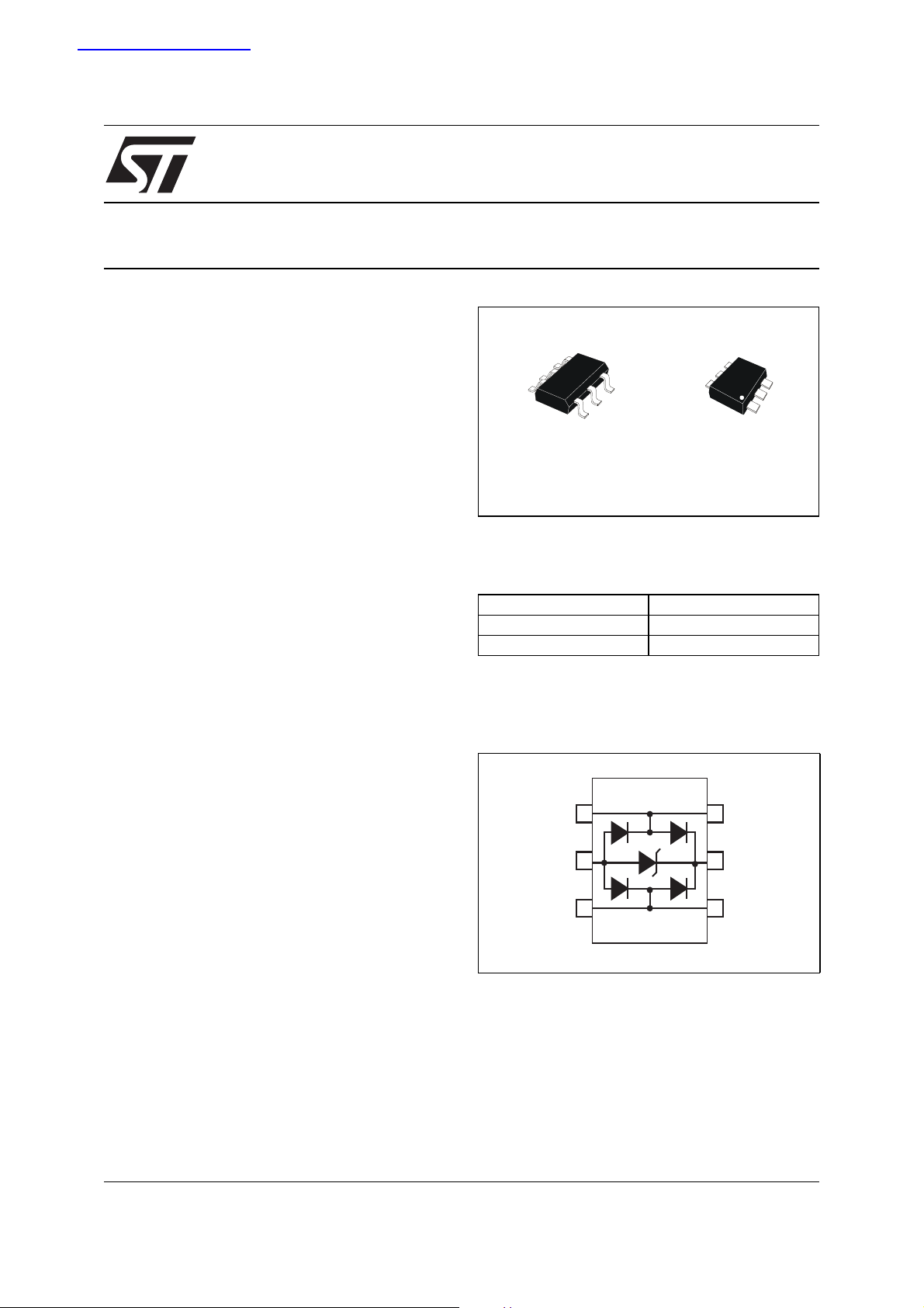
The USBLC6-2P6 and USBLC6-2SC6 are two
monolithic Application Specific Devices dedicated
to ESD protection of high speed interfaces such as
USB2.0, Ethernet links and Video lines.
The very low line capacitance secures a high level
of signal integrity without compromising in
protection sensitive chips against the most
stringent characterized ESD strikes.
FEATURES
■ 2 data lines protection
■ Protects V
■ Very low capacitance: 3.5pF max
■ Very low leakage current: 1µA max
■ SOT-666 and SOT23-6L packages
■ RoHS compliant
BUS
USBLC6-2
VERY LOW CAPACITANCE
ESD PROTECTION
SOT23-6L
USBLC6-2SC6
Table 1: Order Codes
Part Number Marking
USBLC6-2SC6 UL26
USBLC6-2P6 F
Figure 1: Functional Diagram
SOT-666
USBLC6-2P6
BENEFITS
■ Very low capacitance between lines to GND for
optimized data integrity and speed
■ Ultra low PCB space consuming: 2.9mm² max
for SOT-666 package and 9mm² max for
SOT23-6L package
■ Enhanced ESD protection: IEC61000-4-2 level
4 compliance guaranteed at device level,
hence greater immunity at system level
■ ESD protection of V
. Allows ESD current
BUS
flowing to Ground when ESD event occurs on
data line
■ High reliability offered by monolithic integration
■ Very low leakage current for longer operation
of battery powered devices
■ Fast response time
■ Consistant D+/D- signal balance
- Best capacitance matching tolerance I/O to
GND of 0.04pF
- Compliance with USB2.0 requirement (<1pF)
June 2005
11
I/O1 I/O1
2
GND V
3
I/O2 I/O2
6
5
BUS
4
COMPLIES WITH THE FOLLOWING STANDARDS:
■ IEC61000-4-2 level 4:
15kV (air discharge)
8kV (contact discharge)
REV. 2
1/11
Page 2
USBLC6-2
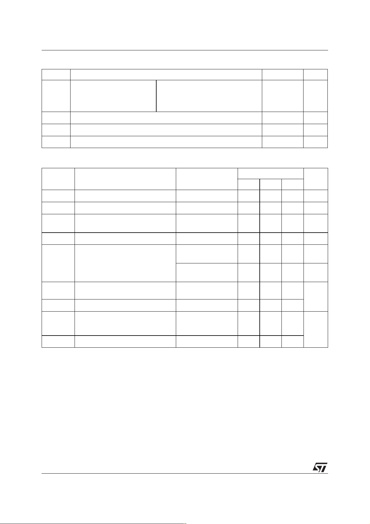
Table 2: Absolute Ratings
Symbol Parameter Value Unit
At device level:
V
Peak pulse voltage
PP
IEC61000-4-2 air discharge
IEC61000-4-2 contact discharge
MIL STD883C-Method 3015-6
15
15
25
kV
T
T
T
Table 3: Electrical Characteristics (T
Storage temperature range -55 to +150 °C
stg
Maximum junction temperature 125 °C
j
Lead solder temperature (10 seconds duration) 260 °C
L
= 25°C)
amb
Symbol Parameter Test Conditions
V
RM
I
RM
V
BR
V
V
CL
Reverse stand-off voltage 5 V
V
Leakage current
Breakdown voltage between V
and GND
Forward voltage
F
BUS
= 5V
RM
= 1mA
I
F
I
= 10mA
F
= 1A, tp = 8/20µs
I
PP
Any I/O pin to GND
Clamping voltage
I
= 5A, tp = 8/20µs
PP
Any I/O pin to GND
C
i/o-GND
∆C
Capacitance between I/O and GND
i/o-GND
V = 0V F = 1MHz
any I/O pin to GND
V = 0V F = 1MHz
C
i/o-i/o
Capacitance between I/O
between I/O, GND
not connected
Value
Unit
Min. Typ. Max.
1µA
6V
1.1 V
12 V
17 V
2.5 3.5
pF
0.04
1.2 1.7
pF
2/11
∆C
i/o-i/o
0.04
Page 3
USBLC6-2
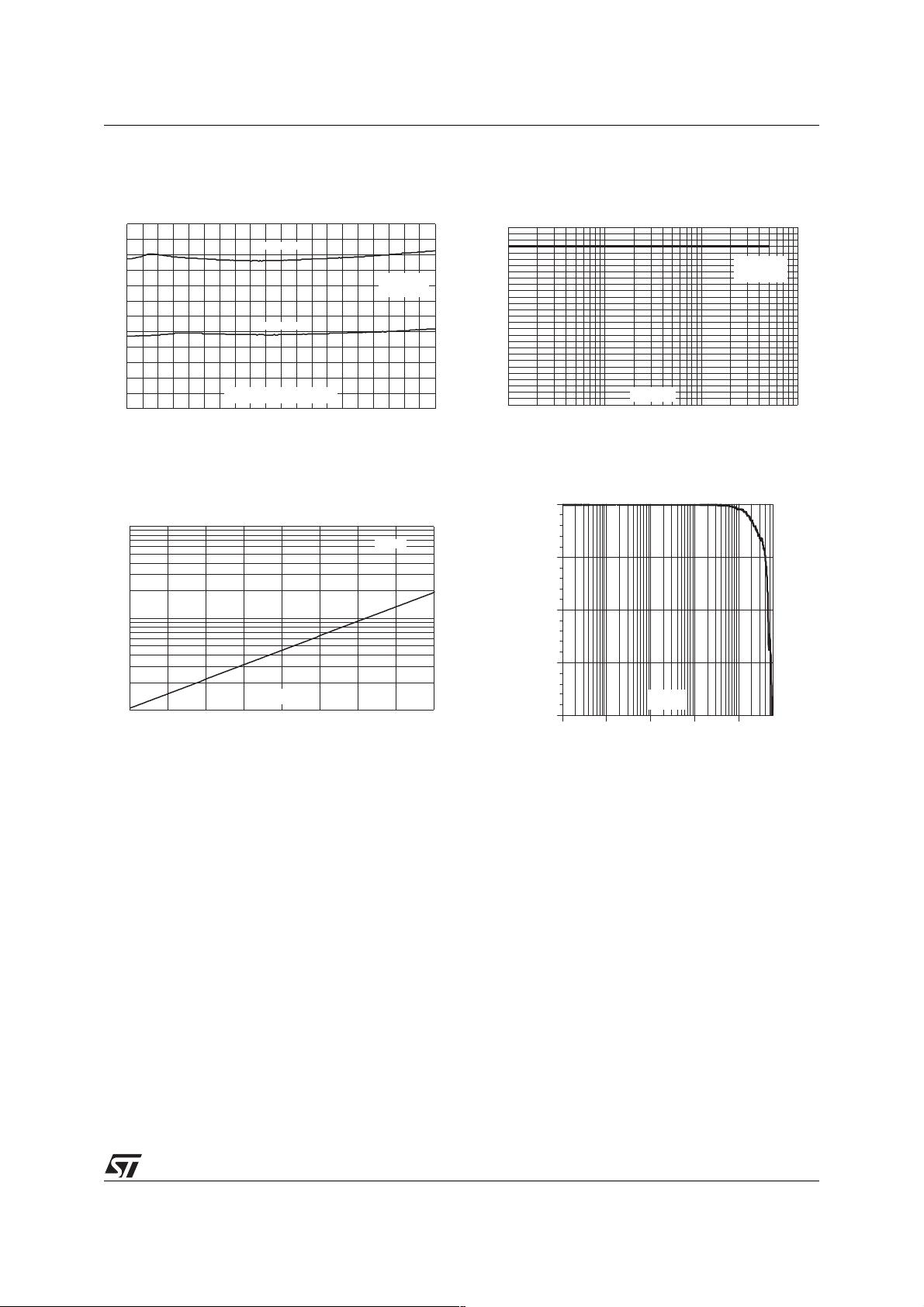
Figure 2: Capacitance versus line voltage
(typical values)
C(pF)
3.0
C =I/O-GND
2.5
2.0
1.5
1.0
0.5
O
C =I/O-I/O
j
F=1MHz
V =30mV
OSC RMS
T =25°C
j
Data line voltage (V)
0.0
0.0 0.5 1.0 1.5 2.0 2.5 3.0 3.5 4.0 4.5 5.0
Figure 4: Relative variation of leakage current
versus junction temperature (typical values)
I[T
] / I [T
100
RM j
10
RM j
=25°C]
V =5V
BUS
Figure 3: Line capacitance versus frequency
(typical values)
C(pF)
2.8
2.6
2.4
2.2
2.0
1.8
1.6
1.4
1.2
1.0
0.8
0.6
0.4
0.2
0.0
1 10 100 1000
F(MHz)
V =30mV
OSC RMS
T=25°C
j
V =0V to 3.3V
LINE
Figure 5: Frequency response
0.00
S21(dB)
-5.00
-10.00
T (°C)
1
25 50 75 100 125
j
-15.00
F(Hz)
-20.00
100.0k 1.0M 10.0M 100.0M 1.0G
3/11
Page 4
USBLC6-2
TECHNICAL INFORMATION
1. SURGE PROTECTION
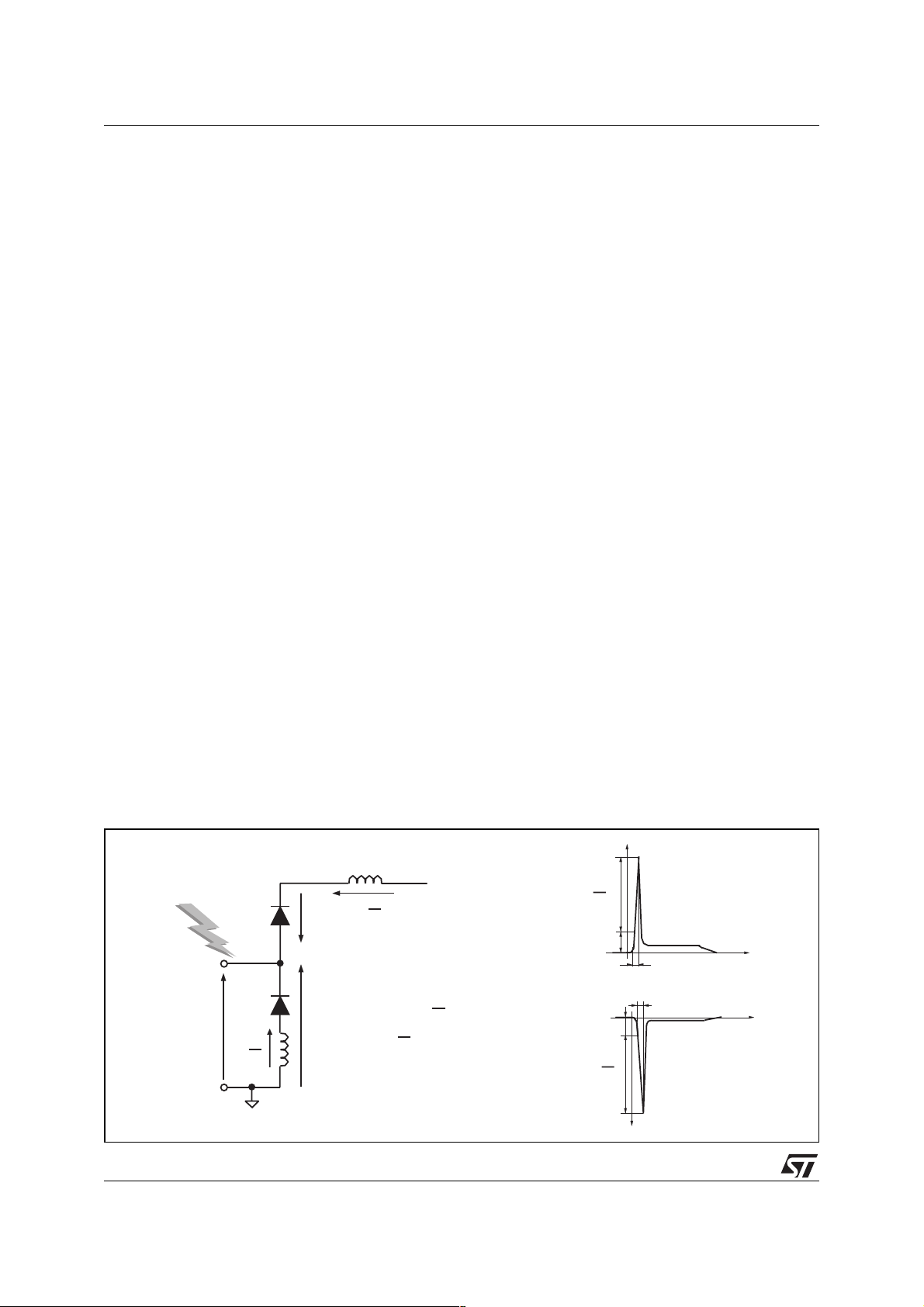
The USBLC6-2 is particularly optimized to perform surge protection based on the rail to rail topology.
The clamping voltage V
with: V
= VT + Rd.I
F
(VF forward drop voltage) / (VT threshold voltage)
We assume that the value of the dynamic resistance of the clamping diode is typically:
= 0.5Ω and VT = 1.2V.
R
d
For an IEC61000-4-2 surge Level 4 (Contact Discharge: V
approximation, we assume that : I
So, we find:
V
CL
V
CL
Note: the calculations do not take into account phenomena due to parasitic inductances.
2. SURGE PROTECTION APPLICATION EXAMPLE
If we consider that the connections from the pin V
two tracks of 10mm long and 0.5mm large; we assume that the parasitic inductances Lw of these tracks
are about 6nH. So when an IEC61000-4-2 surge occurs, due to the rise time of this spike (tr=1ns), the
voltage V
has an extra value equal to Lw.dI/dt.
CL
The dI/dt is calculated as: dI/dt = Ip/tr = 24 A/ns
The overvoltage due to the parasitic inductances is: Lw.dI/dt = 6 x 24 = 144V
By taking into account the effect of these parasitic inductances due to unsuitable layout, the clamping
voltage will be :
V
CL
V
CL
We can reduce as much as possible these phenomena with simple layout optimization.
It’s the reason why some recommendations have to be followed (see paragraph “How to ensure a good
ESD protection”).
can be calculated as follow :
CL
+ = V
V
CL
V
- = - VF for negative surge
CL
p
+ VF for positive surge
BUS
= Vg / Rg = 24A.
p
+ = +17V
- = -12V
+ = +17 + 144 = 161V
- = -12 - 144 = -156V
=8kV, Rg=330Ω), V
g
to VCC and from GND to PCB GND are done by
BUS
= +5V, and if in first
BUS
Figure 6: ESD behavior; parasitic phenomena due to unsuitable layout
183V
di
Lw
dt
VV
+
CC F
-V
di
-Lw
dt
-178V
4/11
ESD
SURGE
VI/O
Lw
Lw
F
V+ =
CL
V- =
CL
Lw
di
dt
V +V +Lw
BUS F
di
-V -Lw
F
dt
+V
CC
di
surge >0
dt
surge <0
V
BUS
V
I/O
di
dt
GND
F
V
tr=1ns
tr=1ns
CL
V
+
POSITIVE
SURGE
NEGATIVE
SURGE
-
CL
t
t
Page 5
USBLC6-2
3. HOW TO ENSURE A GOOD ESD PROTECTION
While the USBLC6-2 provides a high immunity to ESD surge, an efficient protection depends on the layout
of the board. In the same way, with the rail to rail topology, the track from the V
+V
and from the GND pin to GND must be as short as possible to avoid overvoltages due to parasitic
CC
phenomena (see figure 6).
It’s often harder to connect the power supply near to the USBLC6-2 unlike the ground thanks to the ground
plane that allows a short connection.
To ensure the same efficiency for positive surges when the connections can’t be short enough, we
recommend to put close to the USBLC6-2, between V
and ground, a capacitance of 100nF to prevent
BUS
from these kinds of overvoltage disturbances (see figure 7).
The add of this capacitance will allow a better protection by providing during surge a constant voltage.
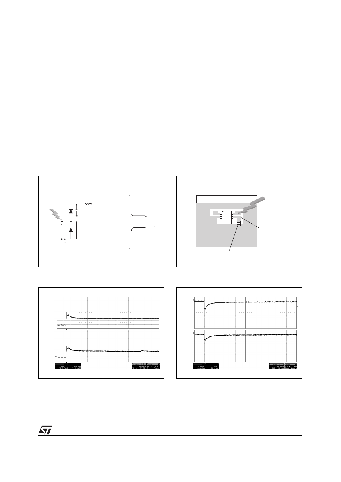
The figures 8, 9 and 10 show the improvement of the ESD protection according to the recommendations
described above.
pin to the power supply
BUS
Figure 7: ESD behavior: optimized layout and
add of a capacitance of 100nF
V+
CL
ESD
SURGE
I/O
VI/O
REF1=GND
Lw
C=100nF
V+ V
V+= surge >0
CL CC F
VV
-- =
CL F
REF2=+V
surge <0
V-
CL
POSITIVE
SURGE
NEGATIVE
SURGE
t
t
CC
Figure 9: Remaining voltage after the
USBLC6-2 during positive ESD surge
Vin
Figure 8: ESD behavior: measurements
conditions (with coupling capacitance)
ESD
TEST BOARD
USBLC6-2SC6
C=100nF
SURGE
+5V
Figure 10: Remaining voltage after the
USBLC6-2 during negative ESD surge
Vin
Vout
Vout
IMPORTANT:
A main precaution to take is to put the protection device closer to the disturbance source (generally the
connector).
Note: The measurements have been done with the USBLC6-2 in open circuit.
5/11
Page 6
USBLC6-2
4. CROSSTALK BEHAVIOR
4.1. Crosstalk phenomena
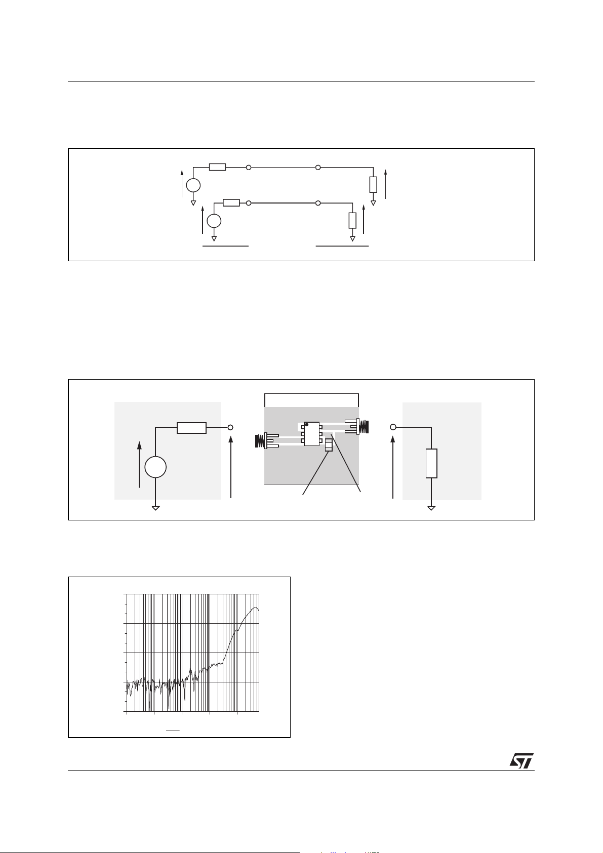
Figure 11: Crosstalk phenomena
R
V
G1
G1
R
G2
Line 1
Line 2
β
α
VG1V
+
R
L1
1
G2
12
V
G2
DRIVERS
R
L2
RECEIVERS
The crosstalk phenomena are due to the coupling between 2 lines. The coupling factor (β
α
β
+
V
V
G2
G1
21
2
or β21)
12
increases when the gap across lines decreases, particularly in silicon dice. In the example above the
expected signal on load R
This part of the V
signal represents the effect of the crosstalk phenomenon of the line 1 on the line 2.
G1
is α2VG2, in fact the real voltage at this point has got an extra value β21VG1.
L2
This phenomenon has to be taken into account when the drivers impose fast digital data or high frequency
analog signals in the disturbing line. The perturbed line will be more affected if it works with low voltage
signal or high load impedance (few kΩ).
Figure 12: Analog crosstalk measurements
TRACKING GENERATOR
50
Ω
Vg
Vin
TEST BOARD
C=100nF
USBLC6-2SC6
V
SPECTRUM ANALYSER
Vout
BUS
50
Ω
Figure 12 gives the measurement circuit for the analog application. In usual frequency range of analog
signals (up to 240MHz) the effect on disturbed line is less than -55 dB (please see figure 13).
Figure 13: Analog crosstalk results
As the USBLC6-2 is designed to protect high
speed data lines, it must ensure a good transmission of operating signals. The frequency response
(figure 5) gives attenuation information and shows
that the USBLC6-2 is well suitable for data line
0.00
-30.00
APLAC 7.91 User: ST Microelectronics Jan 12 2005
dB
Analog Crosstalk
transmission up to 480 Mbit/s while it works as a
-60.00
filter for undesirable signals like GSM (900MHz)
frequencies, for instance.
-90.00
-120.00
100.0k 1.0M 10.0M 100.0M 1.0G
Attenuation
6/11
f/Hz
Page 7
5. APPLICATION EXAMPLES
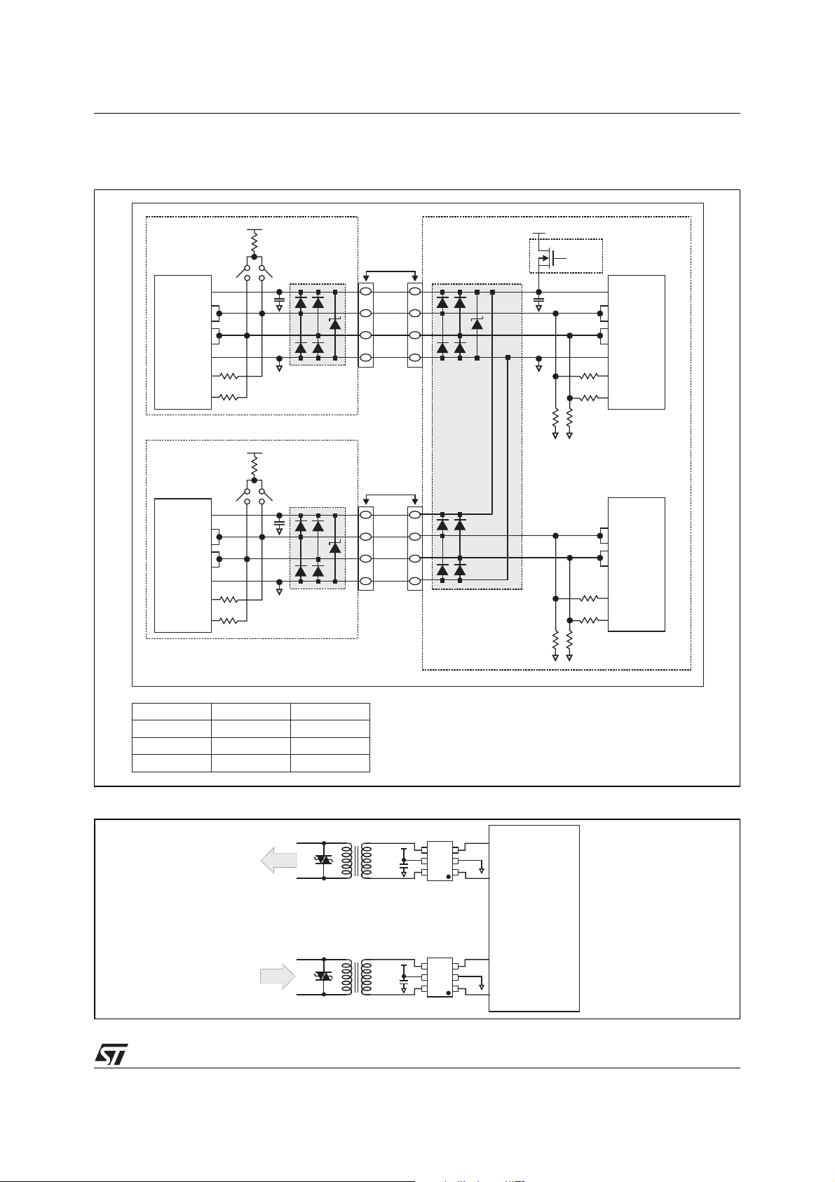
Figure 14: USB2.0 port application diagram using USBLC6-2
USBLC6-2
DEVICEUPSTREAM
TRANSCEIVER
V
BUS
R
X LS/FS
R
X HS
T
X HS
R
X LS/FS -
R
X HS -
T
X HS -
GND GND
T
X LS/FS
T
X LS/FS -
DEVICEUPSTREAM
TRANSCEIVER
V
BUS
R
X LS/FS
R
X HS
T
X HS
R
X LS/FS -
R
X HS -
T
X HS -
GND
T
X LS/FS
T
X LS/FS -
+ 3.3V
R
PU
SW
2
SW
1
+ R
+ R
+ T
USB
connector
V
BUS
D+
+ 5V
D-
R
S
+ T
R
S
USBLC6-2SC6
GND
R
PD
+ 3.3V
R
PU
SW
2
SW
1
+
+
+
USB
connector
V
BUS
D+
D-
R
S
+
R
S
USBLC6-2P6
GND
USBLC6-4SC6
R
PD
Protecting
Bus Switch
R
S
R
S
R
PD
R
S
R
S
R
PD
DOWNSTREAM
HUB-
TRANSCEIVER
V
BUS
+
X LS/FS
+
X HS
+
X HS
R
X LS/FS -
R
X HS -
T
X HS -
+
X LS/FS
T
X LS/FS -
R
+
X LS/FS
R
+
X HS
T
+
X HS
R
X LS/FS -
R
X HS -
T
X HS -
GND
T
+
X LS/FS
T
X LS/FS -
Mode
SW
SW
1
2
ClosedOpenLow Speed LS
OpenClosedFull Speed FS
OpenClosed then openHigh Speed HS
Figure 15: T1/E1/Ethernet protection
Tx
SMP75-8
Rx
SMP75-8
+V
100nF
+V
100nF
CC
USBLC6-2SC6USBLC6-2SC6
DATA
TRANSCEIVER
CC
7/11
Page 8
USBLC6-2
6. PSPICE MODEL
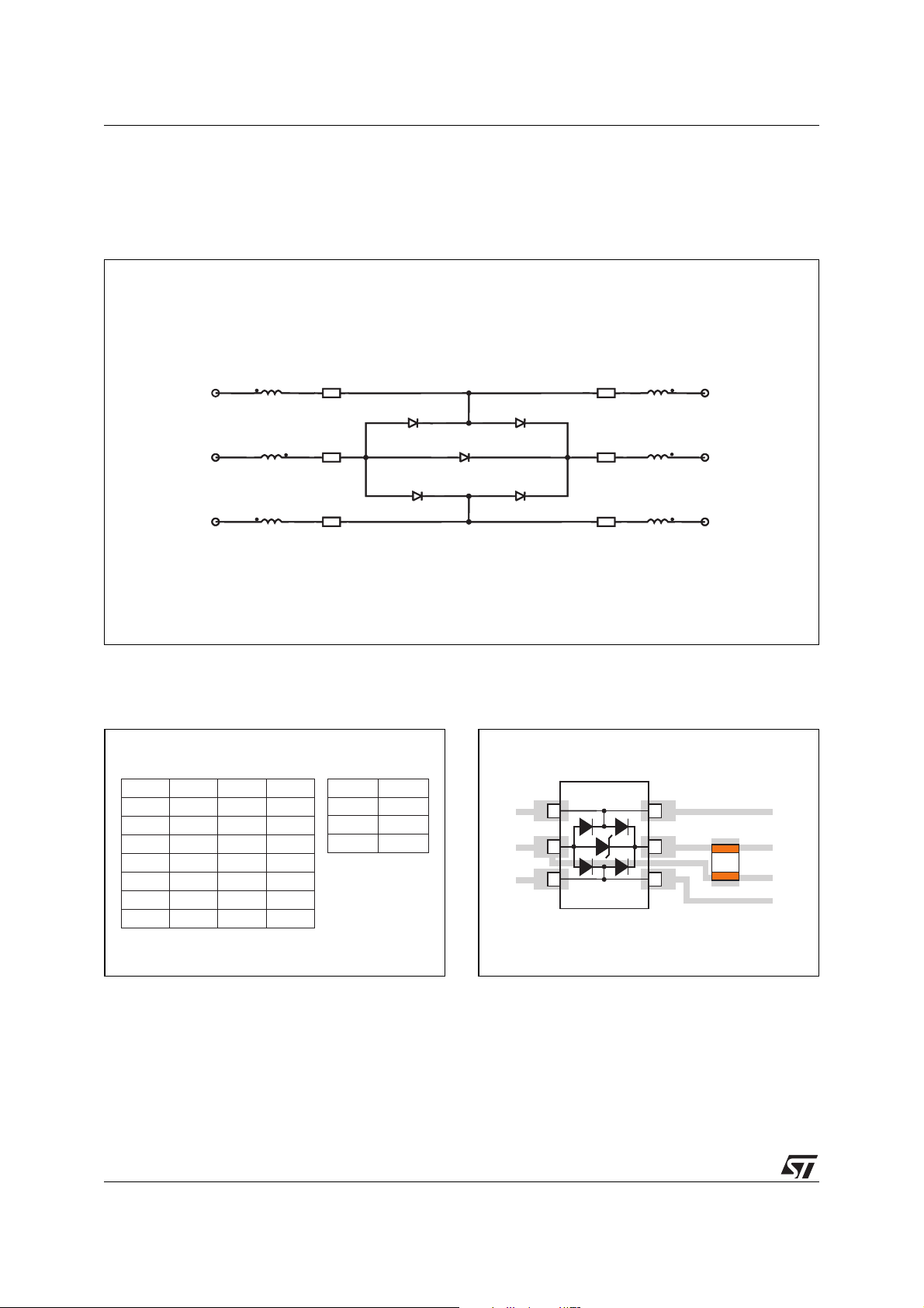
Figure 16 shows the PSPICE model of one USBLC6-2 cell. In this model, the diodes are defined by the
PSPICE parameters given in figure 17.
Figure 16: PSPICE model
D+in
GND
D-in
LI/O
LGND
LI/O
RI/O
MODEL = Dlow MODEL = Dhigh
RGND RI/O
MODEL = Dlow MODEL = Dhigh
RI/O
MODEL = Dzener
RI/O
RI/O
LI/O
D+out
LI/O
VBUS
LI/O
D-out
Note: This simulation model is available only for an ambient temperature of 27°C.
Figure 17: PSPICE parameters Figure 18: USBLC6-2 PCB layout
considerations
Dlow Dhigh Dzener
BV 50 50 7.3
CJ0 0.9p 2.0p 40p
IBV 1m 1m 1m
M 0.3333 0.3333 0.3333
RS 0.2 0.52 0.84
VJ 0.6 0.6 0.6
TT 0.1u 0.1u 0.1u
LI/O 750p
RI/O 110m
LGND 550p
RGND 60m
D+in
GND
D-in
1
USBLC6-2
D+out
V
BUS
D-out
C = 100nF
BUS
8/11
Page 9
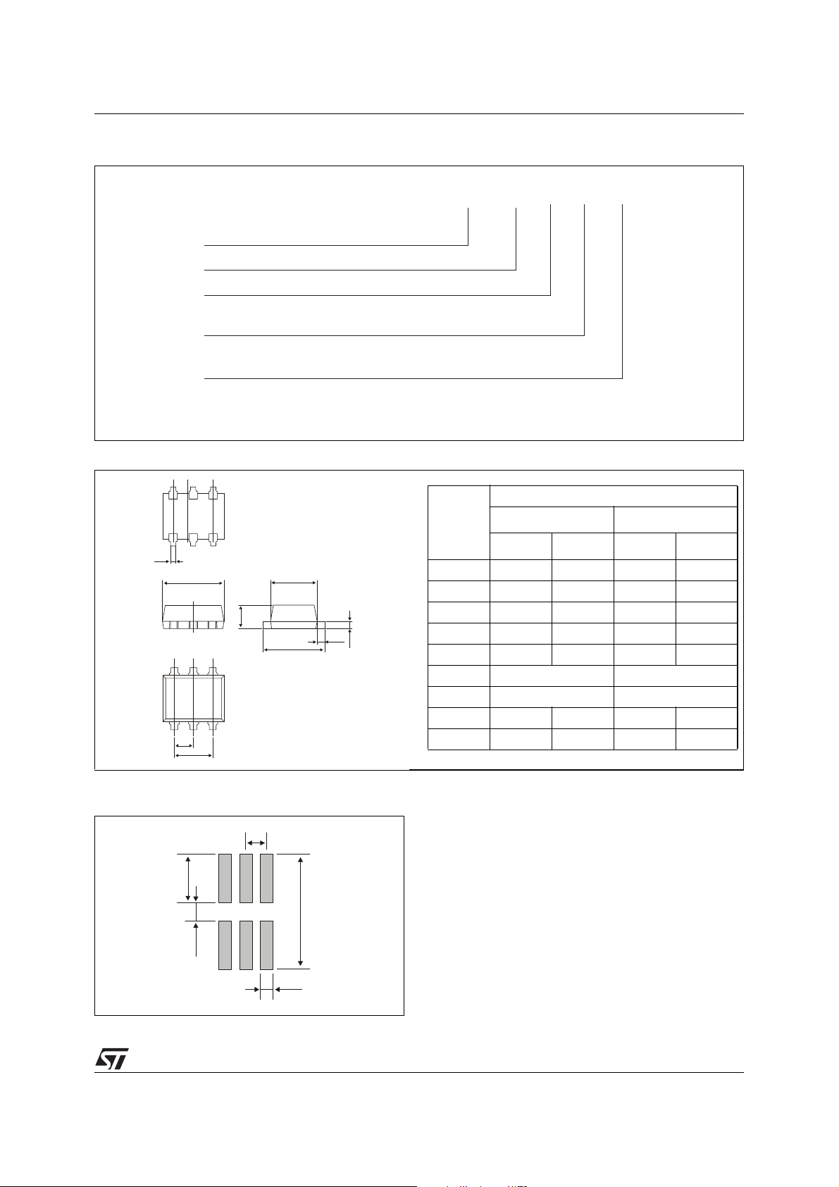
Figure 19: Ordering Information Scheme
Product Designation
Low capacitance
Breakdown Voltage
6 = 6 Volts
Number of lines protected
2 = 2 lines
Packages
SC6 = SOT23-6L
P6 = SOT-666
Figure 20: SOT-666 Package Mechanical Data
bp
D
A
e1
e
E
Lp
He
U
USBLC6-2
USB LC 6 - 2 xxx
DIMENSIONS
REF.
Millimeters
Min.
Max. Min. Max.
A 0.50 0.60 0.020 0.024
bp 0.17 0.27 0.007 0.011
c 0.08 0.18 0.003 0.007
D 1.50 1.70 0.060 0.067
E 1.10 1.30 0.043 0.051
e 1.00 typ. 0.040 typ.
e1 0.50 typ. 0.020 typ.
He 1.50 1.70 0.059 0.067
Lp 0.10 0.30 0.004 0.012
Inches
Figure 21: Foot Print Dimensions (in millimeters)
0.5
1.16
2.75
0.43
0.3
9/11
Page 10
USBLC6-2
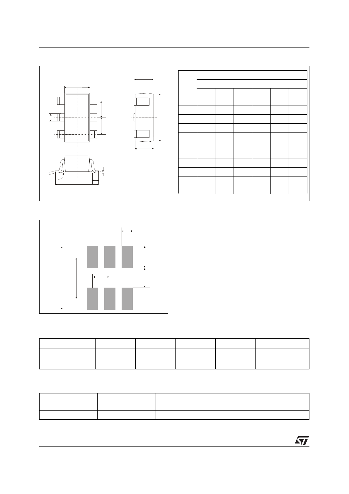
Figure 22: SOT23-6L Package Mechanical Data
A
E
e
B
e
A2
c
θ
H
A1
L
D
Figure 23: Foot Print Dimensions (in millimeters)
0.60
DIMENSIONS
REF.
Millimeters Inches
Min. Typ. Max. Min. Typ. Max.
A 0.90 1.45 0.035 0.057
A1 0 0.10 0 0.004
A2 0.90 1.30 0.035 0.051
b 0.35 0.50 0.014 0.02
C 0.09 0.20 0.004 0.008
D 2.80 3.05 0.110 0.120
E 1.50 1.75 0.059 0.069
e 0.95 0.037
H 2.60 3.00 0.102 0.118
L 0.10 0.60 0.004 0.024
θ 0° 10° 0° 10°
1.20
3.50 2.30
0.95
1.10
Table 4: Ordering Information
Ordering code Marking Package Weight Base qty Delivery mode
USBLC6-2SC6 UL26 SOT23-6L 16.7 mg 3000 Tape & reel
USBLC6-2P6 F SOT-666 2.9 mg 3000 Tape & reel
Table 5: Revision History
Date Revision Description of Changes
14-Mar-2005 1 First issue.
07-Jun-2005 2 Format change to figure 3; no content changed.
10/11
Page 11

USBLC6-2
Information furnished is believed to be accurate and reliable. However, STMicroelectronics assumes no responsibility for the consequences
of use of such information nor for any infringement of patents or other rights of third parties which may result from its use. No license is granted
by implication or otherwise under any patent or patent rights of STMicroelectronics. Specifications mentioned in this publication are subject
to change without notice. This publication supersedes and replaces all information previously supplied. STMicroelectronics products are not
authorized for use as critical components in life support devices or systems without express written approval of STMicroelectronics.
The ST logo is a registered trademark of STMicroelectronics.
All other names are the property of their respective owners
© 2005 STMicroelectronics - All rights reserved
Australia - Belgium - Brazil - Canada - China - Czech Republic - Finland - France - Germany - Hong Kong - India - Israel - Italy - Japan -
Malaysia - Malta - Morocco - Singapore - Spain - Sweden - Switzerland - United Kingdom - United States of America
STMicroelectronics group of companies
www.st.com
11/11
 Loading...