

Page 1
US5881
CMOS Multi-Purpose Switch
US5881 CMOS Multi-Purpose Switch 3901005881 Rev 5.0 24/July/01 Page 1
Features and Benefits
• Chopper stabilized amplifier stage
• New miniature package / thin, high reliability package
• Operation down to 3.5V
• CMOS for optimum stability, quality and cost
Applications
• Solid state switch
• Limit switch
• Current limit
• Interrupter
• Current sensing
Ordering Information
Part No. Temperature Suffix Package Temperature Range
US5881 E SO or UA -40oC to 85oC Extended
US5881 L SO or UA -40oC to 150oC Automotive
*Contact factory or sales representative for legacy temperature options
Description
The US5881 is a unipolar Hall effect sensor IC fabricated from mixed signal CMOS technology. It incorporates advanced chopper stabilization techniques to provide accurate and stable magnetic
switch points. There are many applications for this
sensor in addition to those listed above. The design, specifications and performance have been
optimized for applications of solid state switches.
The output transistor will be switched on (BOP) in
the presence of a sufficiently strong South pole
magnetic field facing the marked side of the package. Similarly, the output will be switched off (BRP)
in the presence of a weaker South field and remain
off with “0” field. The SOT-23 device is reversed
from the UA package. The SOT-23 output transistor will be switched on (BOP) in the presence of a
sufficiently strong North pole magnetic field subjected to the marked face.
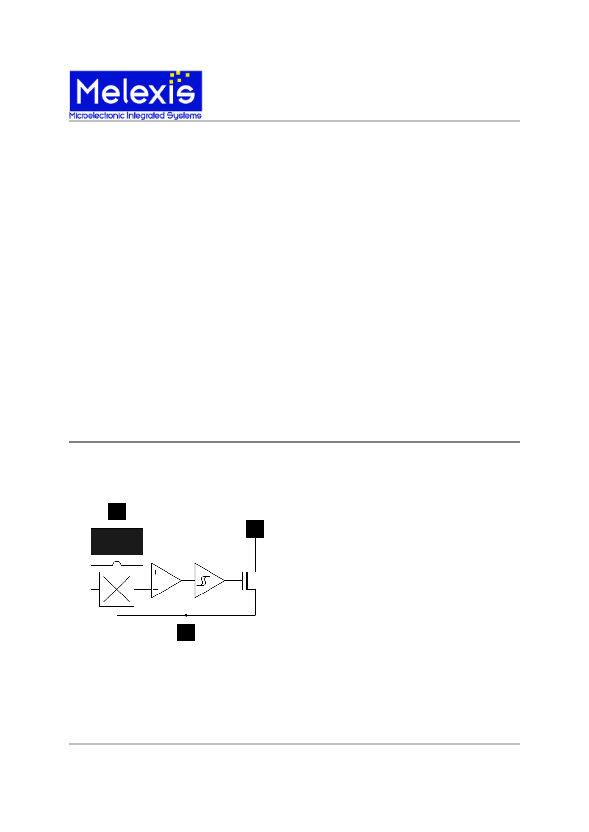
Functional Diagram
Note: This is a static-sensitive device; please observe ESD precautions. Reverse VDD protection is not included. For reverse voltage
protection, a 100Ω resistor in series with VDD is recommended.
Output
GND
V
DD
Voltage
Regulator
Chopper
SO Package
Pin 1 - V
DD
Pin 2 - Output
Pin 3 - GND
UA Package
Pin 1 - V
DD
Pin 2 - GND
Pin 3 - Output
Page 2
US5881 CMOS Multi-Purpose Switch 3901005881 Rev 5.0 24/July/01 Page 2
US5881
CMOS Multi-Purpose Switch
US5881 Electrical Specifications
Parameter Symbol Test Conditions Min Typ Max Units
Supply Voltage VDD Operating 3.5 24 V
Supply Current IDD B<BRP 1.5 2.5 4.0 mA
Saturation Voltage V
DS(on)
I
OUT
= 20 mA, B>BOP 0.4 0.5 V
Output Leakage I
OFF
B<BRP, V
OUT
= 20V 0.01 5.0 ì A
Output Rise Time tr VDD = 12V, RL = 1.1KÙ, CL = 20pf 0.04 ì s
Output Fall Time tf VDD = 12V, RL = 1.1KÙ, CL = 20pf 0.18 ì s
US5881 Magnetic Specifications
Parameter Symbol Test Conditions Min Typ Max Units
Operating Point3 BOP 15 25 30 mT
Release Point BRP 9.5 20 - mT
Hysteresis B
hys
2.0 4.3 5.5 mT
Melexis Inc. reserves the right to make changes without further notice to any products herein to improve reliability, function or design. Melexis does
not assume any liability arising from the use of any product or application of any product or circuit described herein.
Notes:
1. 1 mT = 10 Gauss.
2. The SOT-23 device is reversed from the UA package. The SOT-23 output transistor will be switched
on (BOP) in the presence of a sufficiently strong North pole magnetic field subjected to the
markedface.
3. At –40ºC, maximum B
OP
= 35 mT.
Supply Voltage (Operating), VDD 24V
Supply Current (Fault), IDD 50mA
Output Voltage, V
OUT
24V
Output Current (Fault), I
OUT
50mA
Power Dissipation, PD 100mW
Operating Temperature Range, TA -40°C to 150°C
Storage Temperature Range, TS -65°C to 150°C
Maximum Junction Temp, TJ 175°C
ESD Sensitivity (All Pins) +/- 4KV
Absolute Maximum Ratings
Page 3
US5881
CMOS Multi-Purpose Switch
US5881 CMOS Multi-Purpose Switch 3901005881 Rev 5.0 24/July/01 Page 3
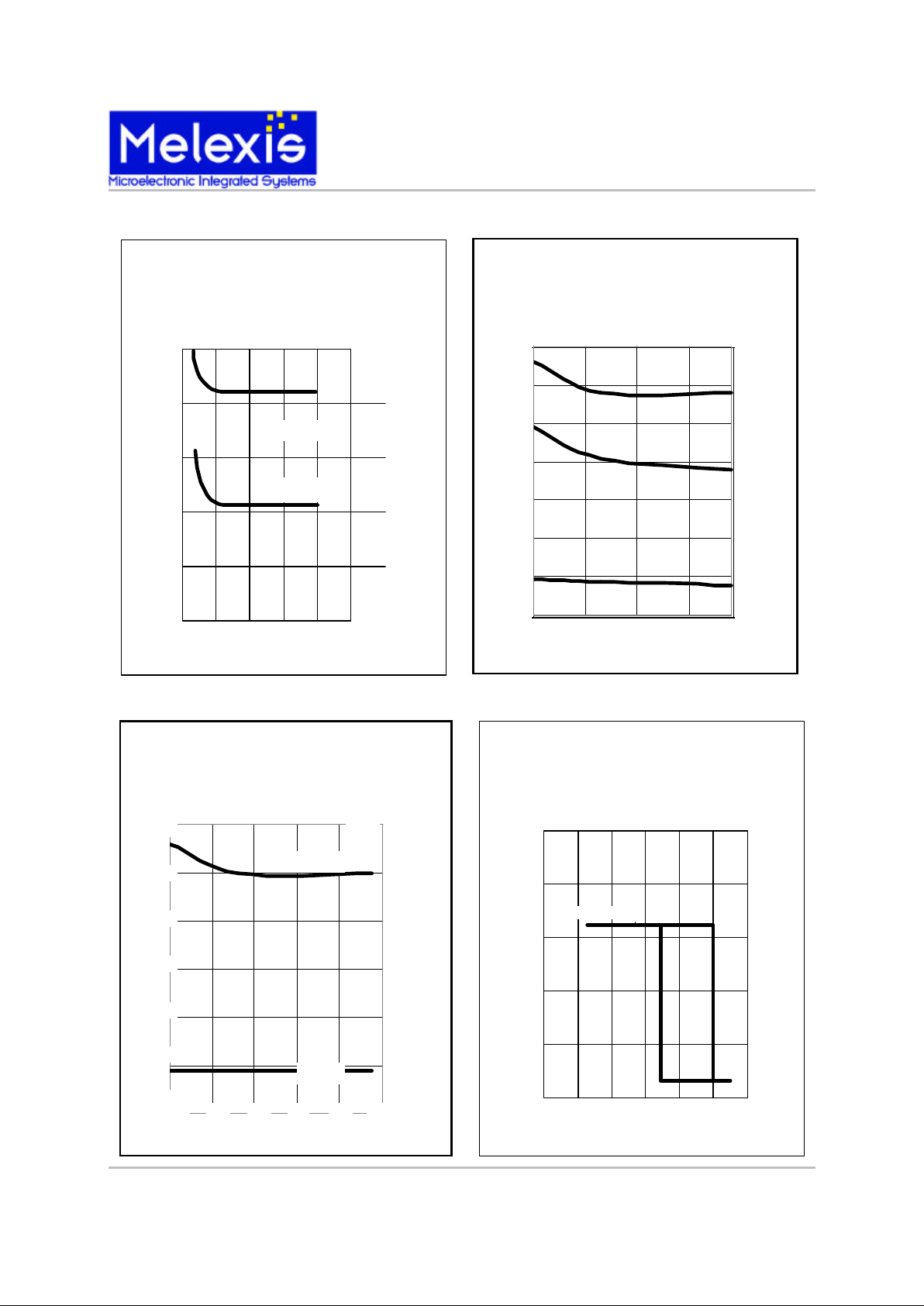
Performance Graphs
35
Flux Density (mT)
Supply Voltage (V)
Typical Magnetic Switch Points
versus
Supply Voltage
5881
15
15
20
25
30
1050 20 25
B
OP
B
RP
10
30
Output Voltage (V)
Flux Density (mT)
Output Voltage
versus
Flux Density
5881
10
6
12
18
24
0-10-20 20 30 40
0
V
DD
V
out
B
OP
B
RP
Typical Magnetic Switch Points
versus Temperature
5881
B
HYS
BRP
BOP
Flux Density (mT)
Temperature (ºC)
40 0 80 120 -40
0
20
25
30
15
10
5
35
Typical Magnetic Switch Points
versus Supply Voltage
Minimum & Maximum Magnetic
Switch Range versus Temperature
Output Voltage versus Flux Density
Flux Density (mT)
-40
5
20
25
30
15
10
35
Temperature (ºC)
40 0 120 160 80
BRP Min
BOP Max
5881
150
Page 4
US5881 CMOS Multi-Purpose Switch 3901005881 Rev 5.0 24/July/01 Page 4
US5881
CMOS Multi-Purpose Switch
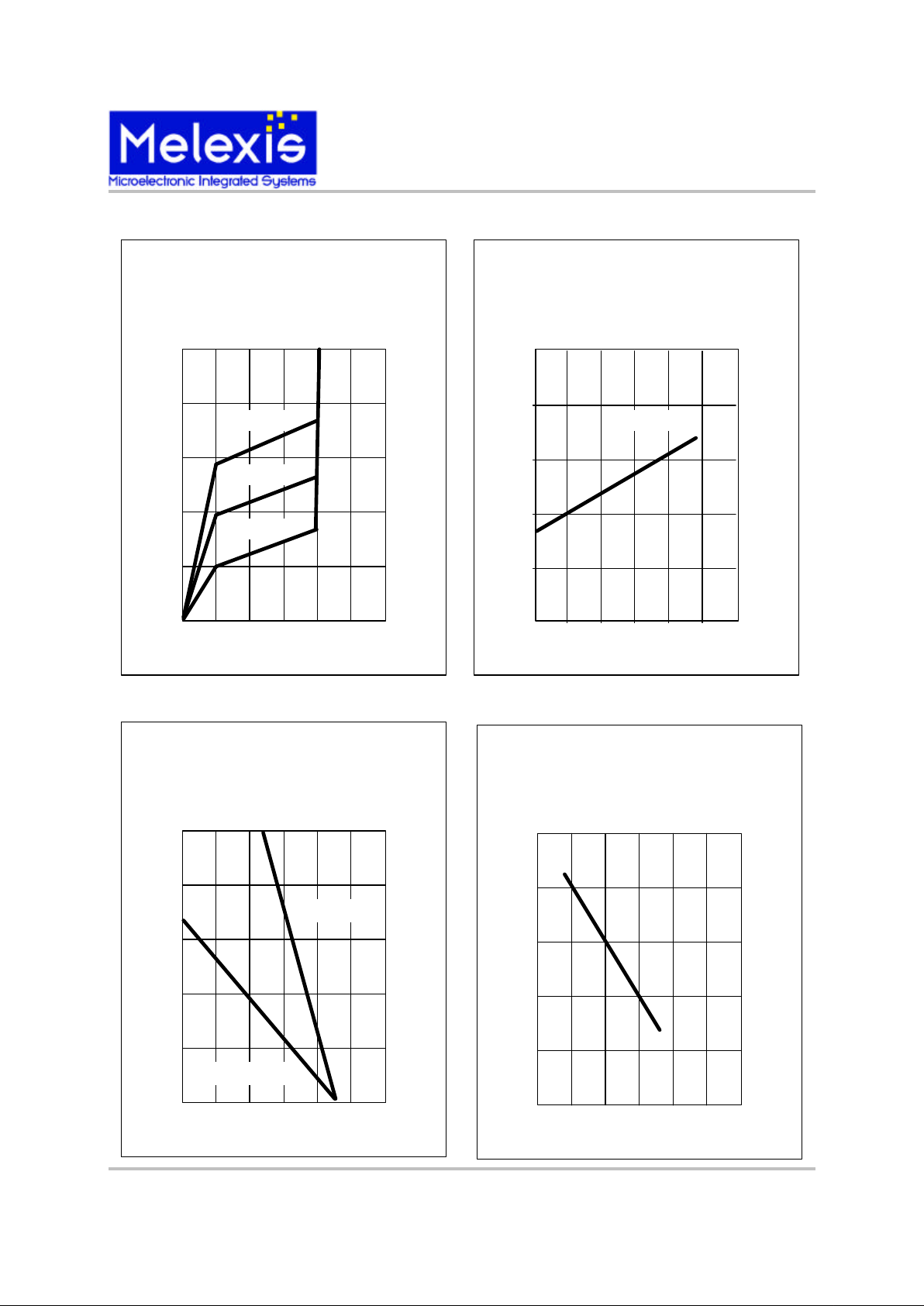
Performance Graphs
280
Solder Temperature (
o
C)
Time in Wave Solder (Seconds)
Wave Soldering Parameters
All Devices
15
200
220
240
260
1050 20 25 30
500
0
Package Power Dissipation (mW)
Temperature (oC)
Power Dissipation
versus
Temperature
All Devices
80
100
200
300
400
0-40 120 160 20040
SO Package
R
θJA
=575oC/W
UA Package
R
θ
JA
=206oC/W
5
0
Supply Current (mA)
Supply Voltage (V)
Typical Supply Current
versus
Supply Voltage
5881
15
1
2
3
4
1050 20 25 30
TA = -40oC
TA = 25oC
TA = 125oC
500
0
V
DS(ON)
(mV)
Temperature (oC)
Typical Saturation Voltage
versus
Temperature
VDD = 12 V, I
OUT
= 20mA
5881
80
100
200
300
400
0-40 120 160 20040
V
DS(ON)
Page 5
US5881
CMOS Multi-Purpose Switch
US5881 CMOS Multi-Purpose Switch 3901005881 Rev 5.0 24/July/01 Page 5
Unique Features
CMOS Hall IC Technology
The chopper stabilized amplifier uses switched capacitor techniques to eliminate the amplifier offset
voltage, which, in bipolar devices, is a major source
of temperature sensitive drift. CMOS makes this advanced technique possible.
The CMOS chip is also much smaller than a bipolar
chip, allowing very sophisticated circuitry to be
placed in less space. The small chip size also contributes to lower physical stress and less power consumption.
Installation
Consider temperature coefficients of Hall IC and
magnetics, as well as air gap life time variations. Observe temperature limits during wave soldering.
Application Comments
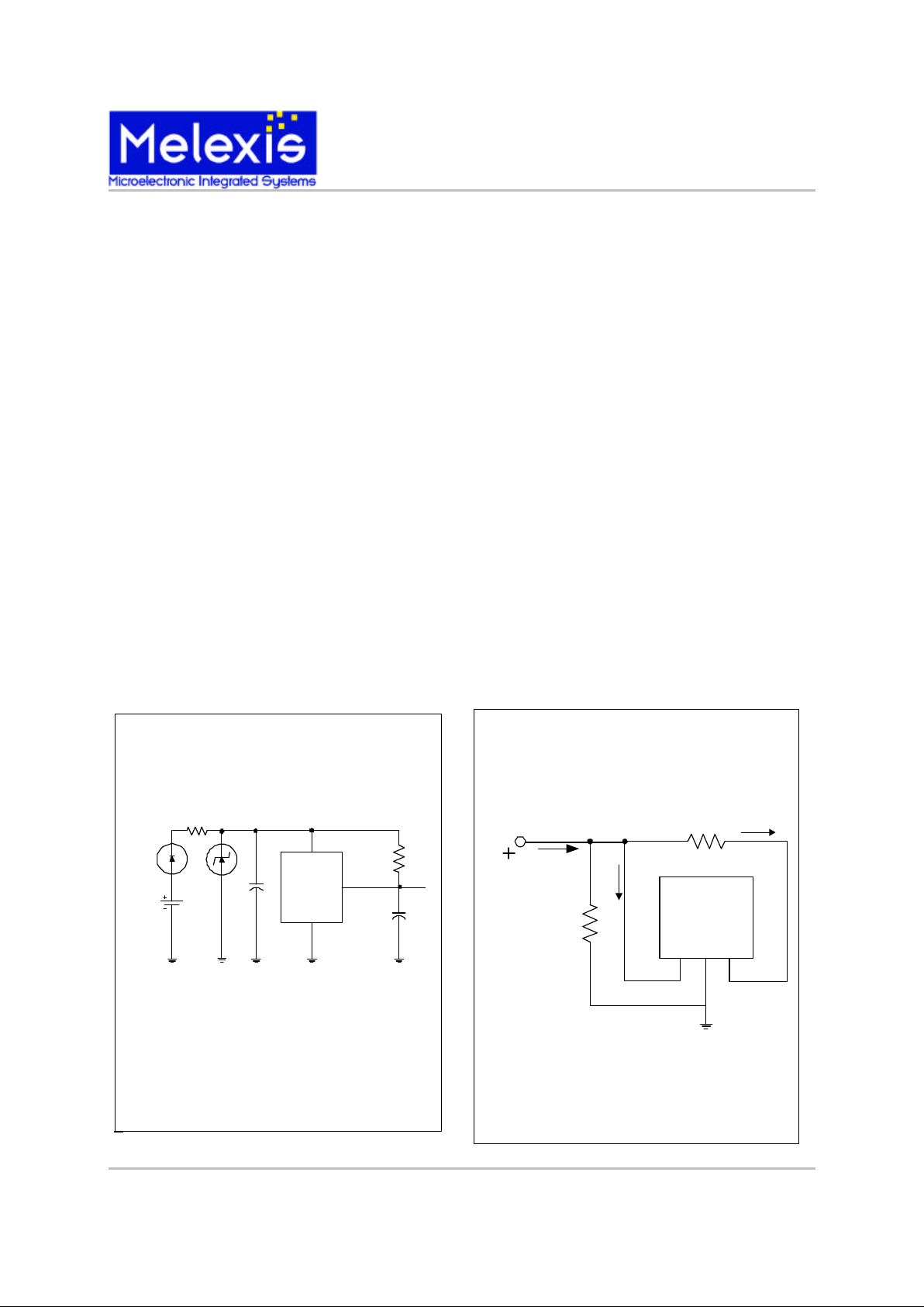
If reverse supply protection is desired, use a resistor
in series with the VDD pin. The resistor will limit the
supply current (Fault), IDD, to 50 mA. For severe
EMC conditions, use the application circuit below.
Applications Examples
Two Wire Optional Current
Biasing Circuit
R
L
R
b
Hall
IC
Iout
I
DD
V
DD
The resistors Rb and RL can be used to bias the input current, IIN. Refer to
the part specification for limiting values. This circuit will help in getting the
precise ON and OFF currents desired.
BRP = Ioff = (VDD / Rb + I
DD
)
BOP = Ion = (Ioff + VDD / RL )
I
IN
Automotive and Severe
Environment Protection Circuit
Hall IC
C1
C2
4.7nF
V
DD
Vss
OUT
R
L
1.2K
Supply
Voltage
D1
R1 100
Ω
Z1
4.7 nF
Page 6
US5881 CMOS Multi-Purpose Switch 3901005881 Rev 5.0 24/July/01 Page 6
US5881
CMOS Multi-Purpose Switch
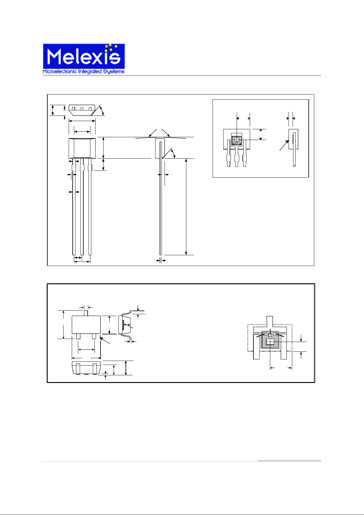
Physical Characteristics
U58
945
1 2 3
*
All Dimensions in millimeters
2.13
1.87
0.45
0.41
Marked
Surface
1.53
1.27
UA Hall Plate / Chip Location
1.60
1.40
45
o
Typical
4.30
3.90
2.64
2.34
0.84
0.63
3.20
2.80
1.75
1.55
0.48
0.43
0.20
0.00
0.41
0.35
1.30
1.24
2.57
2.51
5
o
Typical
45
o
Typical
0.38
Typical
(see note 3)
15.5
14.5
0.41
0.35
UA Package Dimensions
* MARKING:
Line 1:
1st digit (U) = Supplier (Melexis)
2nd and 3rd digits (58) = Series (5880)
Line 2:
1st digit (9) = Year (1999)
2nd and 3rd digits(45) = Week of Year
PINOUT:
Pin 1 V
DD
Pin 2 GND
Pin 3 Output
NOTES:
1.) Controlling dimension: mm.
2.) Leads must be free of flash and
plating voids.
3.) Do not bend leads within 1mm of
lead to package interface.
4.) Package dimensions exclude
molding flash.
5.) Tolerance is +/- 0.254 mm unless
otherwise specified.
SOT-23 Hall Plate /
Chip Location
(Bottom View)
SOT-23 Package Dimensions
(Top View)
NOTES:
1. MARKING:
1st Digit (1) = Series (1880)
2nd Digit(6) = Year - 1996
Last Digits (51) = Week of Year
2. PINOUT (See Top View at left):
Pin 1 VDD
Pin 2 Output
Pin 3 GND
3. Controlling dimension: mm.
4. Lead thickness after solder plating will be 0.254
mm maximum.
5. Package dimensions exclude molding flash.
6. The end flash shall not exceed 0.127 mm on each
side of package.
7. Tolerance is +/- 0.254 mm unless otherwise
specified.
1.55
1.45
0.95
0.85
1651
1.30
1.00
0.10
0.00
3.10
2.70
3.00
2.60
0.50
0.35
1.80
1.50
chip
0.66
0.56
0.20
MIN
0.25
0.10
2.10
1.70
0.90
0.70
*
1 2
3
Pin #
For the latest version of this document,
Go to our website at:
WWW.melexis.com
Or for additional information
Contact Melexis Direct:
Europe and Japan USA and rest of the world
E-mail: [email protected] E-mail: [email protected]
Phone: 011-32-13-670-780 Phone: (603)-223-2362
 Loading...