

Page 1
US1205
300 mA LOW DROPOUT POSITIVE
ADJUSTABLE REGULATOR
PRELIMINARY DATASHEET
FEATURESFEATURES
SOT23 package
Stable with 2.2uF ceramic capacitor
1% Voltage Reference Accuracy
Only 270mV Dropout at 300 mA
170mV Dropout at 150mA
10nA Quiescent Current in Shutdown
Current Limit and Thermal Shutdown
Logic input Enable pin
APPLICATIONSAPPLICATIONS
Laptop, Notebook & Palmtop computers
Battery powered Equipments
PCMCIA Vcc & Vpp regulator
Concumer Electronics
High Efficiency Linear Power Supplies
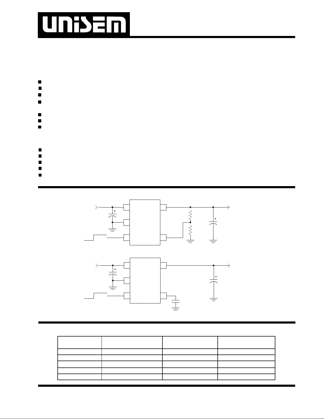
TYPICAL APPLICATIONTYPICAL APPLICATION
Vin Vout
C1
2.2uF
S.D.
Enable
Vin
1
Gnd
2
En
3 4
Vout
Adj
DESCRIPTIONDESCRIPTION
The US1205 device is an efficient linear voltage regulator with better than 1% initial voltage accuracy, very low
dropout voltage and very low ground current designed
especially for hand held, battery powered applications.
Other features of the device are; TTL compatible enable/
shutdown control input, current limiting and thermal
shutdown.
The US1205 is available in fixed and adjustable output
voltage versions in a small SOT23-5 package.
5
R1
Vo=1.242 X (1+R1/R2)
C2
R2
2.2uF
1205app1-1.1
Typical application of the US1205 ajustable.
3.3V 2.5V
C1
2.2uF
S.D. Enable
Vin
1
Gnd
2
En
3 4
Vout
Byp
5
C2
2.2uF
1205app2-1.2
C3
1000pF
Typical application of the US1205 Fixed voltage.
PACKAGE ORDER INFORMATIONPACKAGE ORDER INFORMATION
Tj (°C) 5 LEAD SOT23 Output
SOT 23 Marking Voltage
0 TO 125 US1205CL AT00 Adj
0 TO 125 US1205-25CL AT25 2.5 V
0 TO 125 US1205-30CL AT30 3.0 V
0 TO 125 US1205-33CL AT33 3.3 V
0 TO 125 US1205-36CL AT36 3.6 V
Rev. 1.4
9/25/00
2-1
Page 2
US1205
ABSOLUTE MAXIMUM RATINGSABSOLUTE MAXIMUM RATINGS
Input Voltage (Vin) ............................................................. 10V
Enable Input Voltage ........................................................... 10V
Storage Temperature Range ................................ -65°C TO 150°C
Operating Junction Temperature Range ...................... 0°C TO 150°C
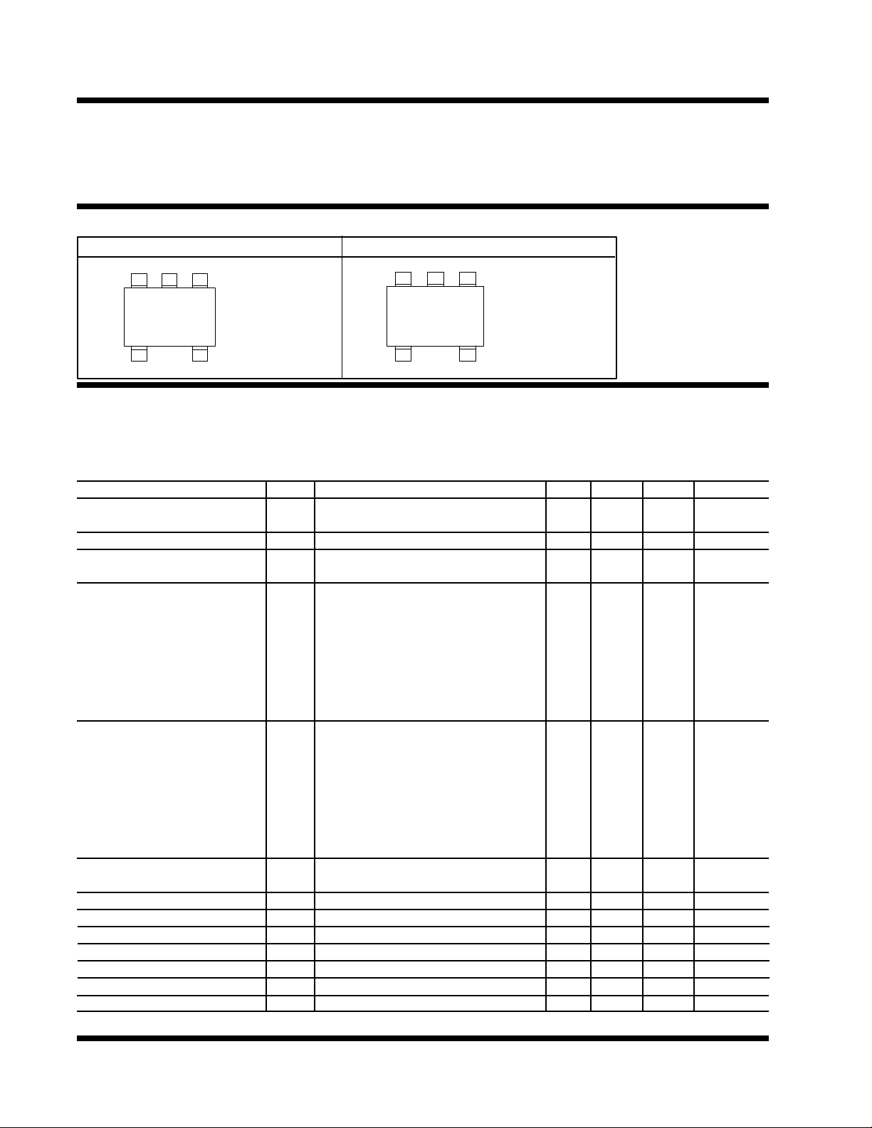
PACKAGE INFORMATIONPACKAGE INFORMATION
5 PIN SOT23 ( L ) Adjustable 5 PIN SOT23 ( L ) Fixed
En
En
Gnd Vin
3 2 1
Gnd Vin
3 2 1
AT00
4 5
Adj
Vout
θJA=220°C/W
ATxx
4 5
Byp
Vout
θJA=220°C/W
ELECTRICAL SPECIFICATIONSELECTRICAL SPECIFICATIONS
Unless otherwise specified ,these specifications apply over ,Cin=Co=22uF, Io=100uA, Vinmin=2.5V(Adjustable
devices) Vin=Vo+1V(for fixed voltage devices), Vout=Vfb (for adjustable version only), Cbyp=470pF(for fixed output
versions only), Venb=2V and Ta=25°C. Typical values refer to Ta=25 °C.Low duty cycle pulse testing are used
which keeps junction and case temperatures equal to the ambient temperature.
PARAMETER SYM TEST CONDITION MIN TYP MAX UNITS
Reference Voltage Vo -1 1 %
See Table 1 for typical values (Note 4) -2 2
Line Regulation dVi Vo+1V<Vin<10 0.005 %/V
Load Regulation (note 1) dVL 1mA<Io<100mA 0.8 %
100mA<Io<300mA 0.1 %
Dropout Voltage (note 2) dVio Io=100uA 10 50 mV
Io=100uA (Note 4) 13 70 mV
Io=50mA 85 110 mV
Io=50mA (Note 4) 100 140 mV
Io=150mA 170 220 mV
Io=150mA (Note 4) 204 260 mV
Io=300mA 270 350 mV
Io=300mA (Note 4) 324 400 mV
Ground Current (Note 3) Iq Ven=2V, Io=100uA 120 160 uA
Io=100uA (Note 4) 240 uA
Io=50mA 420 600 uA
Io=50mA (Note 4) 540 uA
Io=150mA 2200 2900 uA
Io=150mA (Note 4) 2900 uA
Io=300mA 7200 9500 uA
Io=300mA (Note 4) 9300 uA
Ground Current-S.D Activated Iqsd S.D pin<0.1V 0.1 uA
S.D pin=0.8V 8
Current Limit Icl Vo=0V 320 420 mA
Thermal Regulation dVp Vin=10V, Io=150mA,10 mS PULSE 0.05 %/W
Adjust Pin Current Iadj Vin=2.5V,Vo=Vadj 0.1 uA
Enable pin input LO voltage Venl Regulator OFF 0.8 V
Enable pin input HI voltage Venh Regulator ON 2 V
Enable pin input LO current Venl=0V to 0.8V 0.01 uA
Enable pin input HI current Venh=2V to Vin 20 uA
2-2
Rev. 1.4
9/25/00
Page 3

US1205
Note 1 : Low duty cycle pulse testing with Kelvin con-
nections are required in order to maintain accurate data.
Note 2 : Drop-out voltage is defined as the minimum
differential voltage between Vin and Vout required to maintain regulation at Vout. It is measured when the output
voltage drops 1% below its nominal value.
Note 3 : Ground current is the the regulator quiescent
current plus the pass transistor current. The total current from the supply is the sum of the load current plus
the ground pin current.
Note 4 : The specification applies for the junction temperature of 0 to +125°C.
Pin DescRIPTIONSPin DescRIPTIONS
PIN # PIN SYMBOL PIN DESCRIPTION
4 Adj
(Adjustable only)
4 Byp
(Fixed output only)
5 Vout
2 GND
3 En
1 Vin
A resistor divider from this pin to the Vout pin and ground sets
the output voltage.
A 470 to 1000pF bypass capacitor connected to this pin reduces the output noise.
The output of the regulator .A minimum of 2.2uF with max
ESR of 1 ohm capacitor must be connected from this pin to
ground to insure stability.
Ground pin. This pin must be connected to the lowest potential in the system & all other pins must be at higher potential
with respect to this pin.
Enable pin. A low signal or left open on this pin shuts down the
output.This pin must be tied HI or to Vin for normal operation.
The input pin of the regulator. Typically a large storage capacitor
is connected from this pin to ground to insure that the input
voltage does not sag below the minimumdrop out voltage during the load transient response. This pin must always be higher
than Vout by at least the amount of the dropout voltage and
some margin in order for the device to regulate properly.
5 LEAD Output
SOT 23 Voltage
US1205 1.242V
US1205-25 2.5 V
US1205-30 3.0 V
US1205-33 3.3 V
US1205-36 3.6 V
Table 1- Nominal output voltage v.s. part number
BLOCK DIAGRAMBLOCK DIAGRAM
Vin
Adj
Gnd
1.242V
+
THERMAL
SHUTDOWN
1205blk1-1.1
The output voltage of the adjustable device can be set using:
Vo=1.242 X (1+R1/R2)
Where;
R1=Resistor connected from output to the Adj pin
R2=Resistor connected from Adj pin to GND
Vout
En
Vin
Byp
Gnd
1.242V
THERMAL
+
SHUTDOWN
1205blk2-1.0
Vout
En
Figure 1- US1205 Adjustable block diagram
Rev. 1.4
9/25/00
Figure 2- US1205 Fixed output block diagram
2-3
 Loading...