

Page 1
US1260
3-1
Rev. 1.9
3/22/99
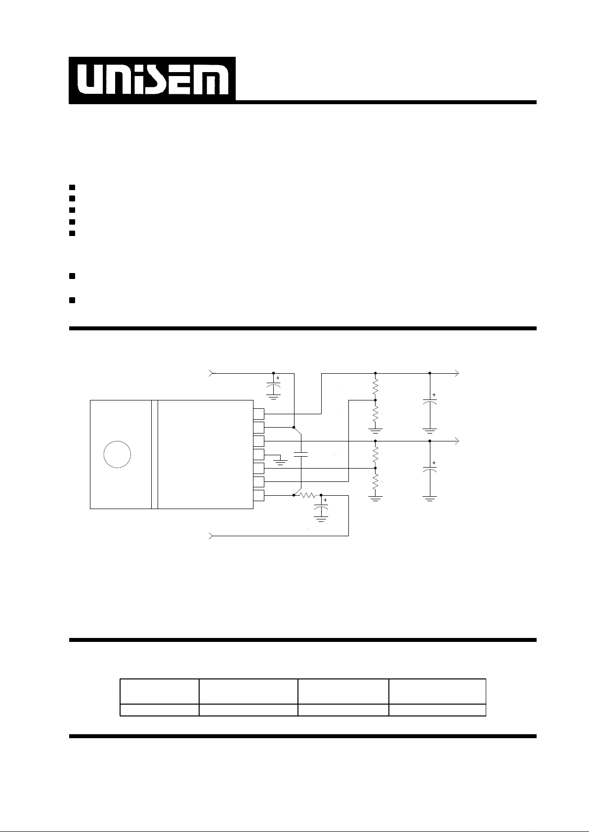
TYPICAL APPLICATIONTYPICAL APPLICATION
FEATURESFEATURES
Guaranteed <1.3V Dropout at 6A (output #2)
Guaranteed <0.6V Dropout at 1A (output #1)
Fast Transient Response
1% Voltage Reference Initial Accuracy
Built in Thermal Shutdown
APPLICATIONSAPPLICATIONS
Providing a single package solution for GTL+
and High Speed Bus Termination
Dual supply P55C applications
DESCRIPTIONDESCRIPTION
The US1260 product using a proprietary process combines a dual low drop out adjustable output regulators in
a single package with one output having a minimum of
6A and the other one having a 1A output current capability. This product is specifically designed to provide well
regulated supplies for low voltage ICs such as 3.3V to
1.5V and 2.5V supplies for the GTL+ termination
and the new clock for Pentium II applications.Other
applications include low cost dual supply for proces-
sors such as Intel P55C where 2.8V and 3.3 V are
needed for the Core and the I/O supplies from the
5V input.
DUAL 6A AND 1A LOW DROPOUT
POSITIVE ADJUSTABLE REGULATOR
Notes: P55C is trade mark of Intel Corp.
Typical application of US1260 in the Pentium ΙΙ design with the 1.5V output providing for GTL+ termination
while 2.5V supplies the clock chip.
Notes: Pentium ΙΙ is trade mark of Intel Corp.
3.3V
2.5V / 1A
1.5V / 6A
C1 R1
R2
R3
R4
C2
C3
US1260
1260app7-1.0
Vctrl
Vfb1
Vfb2
Gnd
Vout2
Vin
Vout1
1
2
3
4
5
6
7
5V
C5
U1
C4
R5
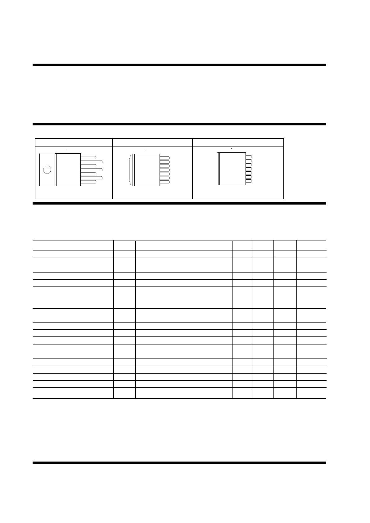
PACKAGE ORDER INFORMATIONPACKAGE ORDER INFORMATION
Tj (°C) 7 PIN PLASTIC 7 PIN PLASTIC 7 PIN PLASTIC
TO220(T) TO263(M) POWER FLEX(P)
0 TO 150 US1260CT US1260CM US1260CP
Page 2
US1260
3-2
Rev. 1.9
3/22/99
Unless otherwise specified ,these specifications apply over ,Cin=1 uF,Cout=10uF,and Tj=0 to 150°C.Typical
values refer to Tj=25°C. Ifl=6A for output #1,and Ifl=1A for output #2. Vfb=Vo for both outputs.Vctrl=Vin=3.3V.
PARAMETER SYM TEST CONDITION MIN TYP MAX UNITS
Vctrl Input Voltage 3.0 V
Reference Voltage Vref Io=10mA,Tj=25°C 1.188 1.200 1.212 V
Io=10mA 1.176 1.200 1.224
Line Regulation Io=10mA,Vout+1.3V<Vin=Vctrl<7V 0.2 %
Load Regulation (note 1) 10mA<Io<Ifl 0.4 %
Dropout Voltage (output #2) Io=4A, Vctrl=4.75V , Vin=3.3V 1.0 V
Io=3A, Vctrl=4.75V , Vin=3.3V 0.7 V
(Note 2) Io=2A, Vctrl=4.75V , Vin=3.3V 0.35 0.5
Dropout Voltage (output #1) Io=1A, Vctrl=4.75V , Vin=3.3V 0.4 0.6 V
(Note 2) Io=1A, Vctrl=Vin=4.75V 1.3
Current Limit (output #2) ICL2 dVo=100mV 6.1 A
Current Limit (output #1) ICL1 dVo=100mV 1.1 A
Thermal Regulation 30 mS pulse,Io=Ifl 0.01 0.02 %/W
Ripple Rejection f=120HZ ,Co=25uF Tantalum
Io=0.5*Ifl 70 dB
Feedback Pin Input Current Ifb Io=10mA 0.02 uA
Temperature Stability Io=10mA 0.5 %
Long Term Stability Ta=125°C,1000 Hrs 0.3 1 %
RMS Output Noise Ta=25°C 10hz<f<10khz 0.003 %Vo
Minimum Load Current(Note 3) 5 mA
Note 3 : Minimum load current is defined as the minimum current required at the output in order for the output voltage to maintain regulation. Typically the resistor
dividers are selected such that it automatically maintains this current.
Note 1 : Low duty cycle pulse testing with Kelvin connections are required in order to maintain accurate data.
Note 2 : Drop-out voltage is defined as the minimum
differential voltage between Vin and Vout required to maintain regulation at Vout. It is measured when the output
voltage drops 1% below its nominal value.
ABSOLUTE MAXIMUM RATINGSABSOLUTE MAXIMUM RATINGS
Input Voltage (Vin) ............................................................. 7V
Power Dissipation ............................................ Internally Limited
Storage Temperature Range ................................ -65°C TO 150°C
Operating Junction Temperature Range ...................... 0°C TO 150°C
PACKAGE INFORMATIONPACKAGE INFORMATION
7 PIN PLASTIC TO220 7 PIN PLASTIC TO263 7 PIN POWER FLEX (P)
θJT =2.7°C/W θJA =60°C/W θJA =30°C/W for 1"sq pad θJA =30°C/W for 1"sq pad
ELECTRICAL SPECIFICATIONSELECTRICAL SPECIFICATIONS
FRONT VIEW
1
2
3
4
5
6
7
Vctrl
Vfb1
Vfb2
Gnd
Vout2
Vin
Vout1
FRONT VIEW
1
2
3
4
5
6
7
Vctrl
Vfb1
Vfb2
Gnd
Vout2
Vin
Vout1
M7
FRONT VIEW
1
2
3
4
5
6
7
Vctrl
Vfb1
Vfb2
Gnd
Vout2
Vin
Vout1
Page 3
US1260
3-3
Rev. 1.9
3/22/99
BLOCK DIAGRAMBLOCK DIAGRAM
Figure 1 - Simplified block diagram of the US1260
PIN DESCRIPTIONSPIN DESCRIPTIONS
PIN # PIN SYMBOL PIN DESCRIPTION
3 Vfb2 A resistor divider from this pin to the Vout #2 pin and ground sets the output
voltage. See application ckt for the divider setting for 1.5V output.
2 Vfb1 A resistor divider from this pin to Vout #1 pin and ground sets the output
voltage.See application ckt for the divider setting for 2.5V output.
5 Vout2 The output #2 (high current) of the regulator. A minimum of 100uF capacitor
must be connected from this pin to ground to insure stability.
7 Vout1 The output #1 (low current) of the regulator. A minimum of 100uF capacitor
must be connected from this pin to ground to insure stability.
6 Vin The power input pin of the regulator. Typically a large storage capacitor is
connected from this pin to ground to insure that the input voltage does not sag
below the minimum drop out voltage during the load transient response. This
pin must always be higher than both Vout pins by the amount of the dropout
voltage(see datasheet) in order for the device to regulate properly.
4 Gnd This pin is connected to GND. It is also the TAB of the package.
1 Vctrl The control input pin of the regulator. This pin via a 10Ω resistor is connected
to the 5V supply to provide the base current for the pass transistor of both
regulators. This allows the regulator to have very low dropout voltage
which allows one to generate a well regulated 2.5V supply from the 3.3V input.
A high frequency, 1 uF capacitor is connected between this pin and Vin pin to
insure stability.
Vctrl
Vin
Gnd
6
1
4
1260blk1-1.1
5 Vout2
7 Vout1
THERMAL
SHUTDOWN
1.20V
2 Vfb1
3 Vfb2
+
Page 4

US1260
3-4
Rev. 1.9
3/22/99
APPLICATION INFORMATIONAPPLICATION INFORMATION
Introduction
The US1260 is a dual adjustable Low Dropout (LDO)
regulator packaged in a 7 pin TO220 which can easily
be programmed with the addition of two external resistors to any voltages within the range of 1.20 to 5.5 V.
This voltage regulator is designed specifically for applications that require two separate regulators such as the
Intel PII processors requiring 1.5V and 2.5 V supplies,
eliminating the need for a second regulator which
results in lower overall system cost. When Vctrl pin
is connected to a supply which is at least 1V higher
than Vin, the dropout voltage improves by 30% which
makes it ideal for applications requiring less than the
standard 1.3V dropout given in the LDO products such
as US10XX series. The US1260 also provides an accurate 1.20V voltage reference common to both regulators
for programming each output voltage. Other features of
the device include; fast response to sudden load current
changes, such as GTL+ termination application for
Pentium II family of microprocessors. The US1260
also includes thermal shutdown protection to protect the
device if an overload condition occurs.
Output Voltage Setting
The US1260 can be programmed to any voltages in the
range of 1.20V to 5.5V with the addition of R1 and R2
external resistors according to the following formula:
Figure 2 - Typical application of the US1260 for
programming the output voltage.
Vout
1260app2-1.0
R2
R1
Vin
Vctrl
Vref
Ib
US1260
Gnd
Vout
Vctrl
Vin
Vfb
1260app3-1.1
R2
R1
Vin
Vctrl
R
L
US1260
Gnd
Vout
Vctrl
Vin
Vfb
Rp
PARASITIC LINE
RESISTANCE
(Only one output is shown here)
V V 1
R
R
V = .
=
& R as shown
OUT REF
2
1
= +
+ ×R I
Wehre : V Typically
I uA Typical
R in figure
B
REF
B
2
1 2
120
0 022.
The US1260 keeps a constant 1.20V between the Vfb
pin and ground pin. By placing a resistor R1 across these
two pins a constant current flows through R1, adding to
the IFB current and into the R2 resistor producing a volt-
age equal to the (1.2/R1)*R2 + IFB* R2 which will be added
to the 1.20V to set the output voltage as shown in the
above equation. Since the input bias current of the amplifier (IFB) is only 0.02uA typically , it adds a very small
error to the output voltage and for most applications can
be ignored. For example, in a typical 1.5V
GTL+application if R1=10.2kΩ and R2=2.55kΩ the error
due to the Iadj is only 0.05mV which is less than 0.004%
of the nominal set point. The effective input imped-
ance seen by the feedback pins (R1 II R2) must always be higher than 1.8kΩ Ω in order for the regula-
tor to start up properly.
Load Regulation
Since the US1260 does not provide a separate ground
pin for the reference voltage, it is not possible to provide
true remote sensing of the output voltage at the load.
Figure 3 shows that the best load regulation is achieved
when the bottom side of R1 resistor is connected directly to the ground pin of US1260 (preferably to the tab
of the device) and the top side of R2 resistor is connected to the load. In fact , if R1 is connected to the load
side, the effective resistance between the regulator and
the load is gained up by the factor of (1+R2/R1) ,or the
effective resistance will be ,Rp(eff)=Rp*(1+R2/R1).It is
important to note that for high current applications, this
can represent a significant percentage of the overall load
regulation and one must keep the path from the regulator to the load as short as possible to minimize this
effect.
Figure 3 - Schematic showing connection for best load
regulation. (Only one output is shown here)
Page 5

US1260
3-5
Rev. 1.9
3/22/99
Stability
The US1260 requires the use of an output capacitor as
part of the frequency compensation in order to make the
regulator stable. Typical designs for the microprocessor applications use standard electrolytic capacitors with
typical ESR in the range of 50 to 100 mΩ and the output
capacitance of 500 to 1000uF. Fortunately as the capacitance increases, the ESR decreases resulting in a
fixed RC time constant. The US1260 takes advantage of
this phenomena in making the overall regulator loop
stable. For most applications a minimum of 100uF aluminum electrolytic capacitor with the maximum ESR of
0.3Ω such as Sanyo, MVGX series ,Panasonic FA series as well as the Nichicon PL series insures both stability and good transient response. The US1260 also
requires a 1 uF ceramic capacitor connected from Vin
to Vctrl and a 10Ω, 0.1W resistor in series with Vctrl pin
in order to further insure stability.
Thermal Design
The US1260 incorporates an internal thermal shutdown
that protects the device when the junction temperature
exceeds the maximum allowable junction temperature.
Although this device can operate with junction temperatures in the range of 150°C ,it is recommended that the
selected heat sink be chosen such that during maximum continuous load operation the junction temperature is kept below this number. Two examples are given
which shows the steps in selecting the proper regulator
heat sink for driving the Pentium II processor GTL+ termination resistors and the Clock IC using 1260 in TO220
or TO-263 packages.
Example # 1
Assuming the following specifications :
The steps for selecting a proper heat sink to keep the
junction temperature below 135°C is given as :
1) Calculate the maximum power dissipation using :
2) Select a package from the datasheet and record its
junction to case (or Tab) thermal resistance.
Selecting TO220 package gives us :
3) Assuming that the heat sink is Black Anodized, calculate the maximum Heat sink temperature allowed :
Assume , θSA = 0.05 °C/W (Heat sink to Case thermal
resistance for Black Anodized)
4) With the maximum heat sink temperature calculated
in the previous step, the Heat Sink to Air thermal resistance θSA is calculated as follows :
5) Next , a heat sink with lower θSA than the one calculated in step 4 must be selected. One way to do this is
to simply look at the graphs of the “Heat Sink Temp
Rise Above the Ambient” vs. the “Power Dissipation” and
select a heat sink that results in lower temperature rise
than the one calculated in previous step. The following
heat sinks from AAVID and Thermaloy meet this criteria.
Air Flow (LFM)
0 100 200 300 400
Thermalloy 7021B 7020B 6021PB 7173D 7141D
AAVID 593101B 551002B 534202B 577102B 576802B
Note : For further information regarding the above companies and their latest product offering and application
support contact your local representative or the numbers listed below:
Thermalloy PH# (214) 243-4321
AAVID PH# (603) 528-3400
V 3.3V
V 1.5 V
V =2.5 V
I 5.4A
I = 0.4 A
T 35 C
IN
OUT 2
OUT 1
OUT 2
OUT 1
A
MAX
MAX
=
=
=
= °
()(
)
( ) ( )
P I V V I V V
P 0.4 + 5.4 3.3 1.5 W
D OUT1 IN OUT1 OUT2 IN OUT2
D
= × − + × −
= × − × − =33 25 10. .
(
)
( )
T T P
T 135 10 2.7 0.05 107.4 C
S J D
S
= − × +
= − × + = °
θ θJC CS
∆
T S A
TTC=−=−=°
107435724..
θ
θ
SA
T
D
SA
P
C W
=
= = °
∆
724
10
724.. /
θ
JC C W
=
°
27. /
Page 6

US1260
3-6
Rev. 1.9
3/22/99
Example # 2 :
Assuming the following specifications :
The steps for selecting a proper heat sink to keep the
junction temperature below 135°C is given as :
1) Calculate the maximum power dissipation using :
2) Assuming a TO-263 surface mount package, the junction to ambient thermal resistance of the package is:
3) The maximum junction temperature of the device is
calculated using the equation below :
Since this is lower than our selected 135°C maximum
junction temperature (150°C is the thermal shutdown of
the device), TO-263 package is a suitable package for
our application.
Layout Consideration
The US1260 like all other high speed linear regulators
need to be properly laid out to insure stable operation.
The most important component is the output capaci-
tor, which needs to be placed close to the output
pin and connected to this pin using a plane connection with a low inductance path.
US1260 in Ultra LDO, Single Output Application
The US1260 can also be used in single supply applications where the difference between input and output is
much lower than the standard 1.5V dropout that is obtainable with standard LDO devices. The schematic in
figure 6 shows the application of the US1260 in a single
supply with the second LDO being disabled.
V 3.3V
V 1.5 V
V =2.5 V
I 1.5A
I = 0.2 A
T 35 C
IN
OUT 2
OUT 1
OUT 2
OUT 1
A
MAX
MAX
=
=
=
= °
()(
)
( ) ( )
P I V V I V V
P 0.2 3.3 2.5 +1.5 3.3 1.5 2.86 W
D OUT1 IN OUT1 OUT2 IN OUT2
D
= × − + × −
= × − × − =
θJA C W for 1"= °30 / square pad area
T T P
T 35+ 2.86 30 =121 C
J A D
J
=+×
= × °
θ
JA
In this application, the US1260 is used on the VGA card
to convert 3.3V supply to 2.7V to power the Intel 740
chip rather than the conventional LDO which due to its
1.5V minimum dropout spec must use the 5V supply to
achieve the same result. The difference is a substantial
decrease in the power dissipation as shown below.
The maximum power dissipation of 740 chip is 5.8W,
which at 2.7V results in Io=5.8/2.7=2.15A
a) Using standard LDO, the power dissipated in the device is;
Pd=(Vin - Vo)*Io=(5-2.7)*2.15=4.94W
Using surface mount TO263 package with 25° C/W junction to air thermal resistance results in:
Tj=Pd*θja + Ta=(4.94)(25) + 25=148 ° C
This is very close to the thermal shutdown of the IC.
b) Using 1260, the power dissipated in the device is drastically reduced by using 3.3V supply instead of 5V
Pd=(Vin - Vo)*Io=(3.3-2.7)*2.15=1.3W
Using surface mount TO263 package with 25° C/W junction to air thermal resistance results in:
Tj=Pd*θja + Ta=(1.3)(25) + 25=57 ° C
A reduction of 91° C in junction temperature.
Page 7

US1260
3-7
Rev. 1.9
3/22/99
TYPICAL APPLICATIONTYPICAL APPLICATION
PENTIUM ΙΙΙΙ APPLICATION
Figure 4 - Typical application of US1260 in the Pentium ΙΙ design with the 1.5V output providing for GTL+
termination while 2.5V supplies the clock chip.
Notes: Pentium ΙΙ is trade mark of Intel Corp.
3.3V
2.5V / 1A
1.5V / 6A
C1 R1
R2
R3
R4
C2
C3
US1260
1260app7-1.0
Vctrl
Vfb1
Vfb2
Gnd
Vout2
Vin
Vout1
1
2
3
4
5
6
7
5V
C5
U1
C4
R5
Ref Desig Description Qty Part # Manuf
U1 Dual LDO Regulator 1 US1260CM Unisem
C1,C3 Capacitor 2 Elect,680uF,EEUFA1A681L Panasonic
C2 Capacitor 1 Elect,220uF,6.3V,ECAOJFQ221 Panasonic
C4 Capacitor 1 Ceramic, 0.1 uF, SMT , 0805 Panasonic
C5 Capacitor 1 Elect,100uF,6.3V,ECAOJFQ101 Panasonic
R1 Resistor 1 11 kΩ , 1%, SMT , 0805 Panasonic
R2,R4 Resistor 2 10.2 kΩ , 1%, SMT , 0805 Panasonic
R3 Resistor 1 2.55 kΩ , 1%, SMT , 0805 Panasonic
R5 Resistor 1 3 Ω , 5%, SMT , 0805 Panasonic
HS1 Heat Sink Use 1" Square Copper Pad area if Iout2<1.7A & Iout1<0.2A
For Iout2<3A & Iout1<0.5A Use US1260CT and Thermalloy
6030B
Page 8

US1260
3-8
Rev. 1.9
3/22/99
TYPICAL APPLICATIONTYPICAL APPLICATION
RAMBUS APPLICATION
Figure 5- Typical application of US1260 in the Rambus design with the 2.5V output providing for memory
termination while 3.3V supplies the on board logic.
Notes:Rambus is trade mark of Rambus Corp.
5V
2.5V
3.3V
C1 R1
R2
R3
R4
C2
C3
US1260
1260app6-1.0
Vctrl
Vfb1
Vfb2
Gnd
Vout2
Vin
Vout1
1
2
3
4
5
6
7
U1
Ref Desig Description Qty Part # Manuf
U1 Dual LDO Regulator 1 US1260CM Unisem
C1,C2,C3 Capacitor 3 Elect,220uF,6.3V,ECAOJFQ221 Panasonic
R1 Resistor 1 11 kΩ , 1%, SMT , 0805 Panasonic
R2,R4 Resistor 2 10.2 kΩ , 1%, SMT , 0805 Panasonic
R3 Resistor 1 17.8 kΩ , 1%, SMT , 0805 Panasonic
HS1 Heat Sink 1" Square Copper Pad area if Iout2<1.2A & Iout1<0.5A
For Iout2<3A & Iout1<0.5A Use Thermalloy 6030B
Page 9

US1260
3-9
Rev. 1.9
3/22/99
TYPICAL APPLICATIONTYPICAL APPLICATION
INTEL I740 GRAPHICS CHIP APPLICATION
Figure 6 - Typical application of US1260 to provide 2.7V from the 3.3V bus for the Intel 740 graphics chip.
Ref Desig Description Qty Part # Manuf
U1 Dual LDO Regulator 1 US1260CM Unisem
C1,C3 Capacitor 2 Elect,680uF,EEUFA1A681L Panasonic
C4 Capacitor 1 Ceramic, 0.1 uF, SMT , 0805 Panasonic
C5 Capacitor 1 Elect,100uF,6.3V,ECAOJFQ101 Panasonic
R4 Resistor 1 10.2 kΩ , 1%, SMT , 0805 Panasonic
R3 Resistor 1 12.7 kΩ , 1%, SMT , 0805 Panasonic
R5 Resistor 1 3 Ω , 5%, SMT , 0805 Panasonic
3.3V
2.7V
C1
R3
R4
C3
US1260
1260app8-1.0
Vctrl
Vfb1
Vfb2
Gnd
Vout2
Vin
Vout1
1
2
3
4
5
6
7
5V
C5
U1
C4
R5
 Loading...