

Datasheet uPD77213GJ-xxx-8EN, uPD77213F1-xxx-DA2, uPD77210GJ-8EN, uPD77210F1-DA2 Datasheet (NEC)
Page 1
DATA SHEET
MOS INTEGRATED CIRCUIT
µµµµ
PD77210, 77213
16-BIT FIXED-POINT DIGITAL SIGNAL PROCESSOR
The µPD77210 and 77213 are 16-bit fixed-point digital signal processors (DSP).
Compared with the existing members of the µPD77111 Family, the µPD77210 Family consumes less power and is
ideal for battery-driven mobile terminal applications such as PDAs and cellular telephones. The µP77210 Family is
DSP is also compatible with the µPD77111 Family at the binary level.
The µPD77210 Family consists of the µPD77210 and 77213. Unless otherwise specified, the µPD77210 Family
refers to the entire family. If there are some differences in function or operation among family products, they are
described under their respective names.
The functions of the µPD77210 Family are described in detail in the following user’s manuals. Refer to these
manuals when designing your system.
PD77210 Family User’s Manual - Architecture: In preparation
µ
PD77016 Family User’s Manual - Instructions: U13116E
µ
FEATURES
• Instruction cycle (operating clock):
PD77210 6.25 ns MIN. (160 MHz MAX.)
µ
PD77213 8.33 ns MIN. (120 MHz MAX.)
µ
• Memory
-Internal instruction memory:
PD77210 :RAM 31.5 Kwords x 32 bits
µ
PD77213 :RAM 15.5 Kwords x 32 bits
µ
ROM 64 Kwords x 32 bits
-Data memory:
PD77210 :RAM 30 Kwords x 16 bits x 2 planes (X and Y data memories)
µ
External memory space 1 Mwords x 16 bits (common to X and Y data memories)
PD77213 :RAM 18 Kwords x 16 bits x 2 planes (X and Y data memories)
µ
ROM 32 Kwords x 16 bits x 2 planes (X and Y data memories)
External memory space 1 Mwords x 16 bits (common to X and Y data memories)
• Peripheral
-Audio serial interface: 1 channel
-Time-division serial interface: 1 channel
-16-bit host interface: 1 channel
-16-bit general-purpose port
The information in this document is subject to change without notice. Before using this document, please
confirm that this is the latest version.
Not all devices/types available in every country. Please check with local NEC representative for
availability and additional information.
Document No. U15203EJ3V0DS00 (3rd edition)
Date Published November 2001 NS CP(K)
Printed in Japan
-16-bit timer: 2 channels
-Peripheral-memory DMA transfer function
-SD (Secure Digital) card interface
:µPD77213 only
The mark shows major revised points.
©
2001
Page 2

• Supply voltage
-DSP core supply voltage: 1.425 to 1.65 V (MAX. operating speed 120 MHz),
1.55 to 1.65 V (MAX. operating speed 160 MHz)
-I/O pin supply voltage: 2.7 to 3.6 V
ORDERING INFORMATION
Parts Number Package
PD77210F1-DA2 161-pin plastic fine pitch BGA (10 x 10)
µ
PD77210GJ-8EN 144-pin plastic LQFP (fine pitch) (20 x 20)
µ
PD77213F1-xxx-DA2 161-pin plastic fine pitch BGA (10 x 10)
µ
PD77213GJ-xxx-8EN 144-pin plastic LQFP (fine pitch) (20 x 20)
µ
Remark xxx indicates ROM code suffix.
µµµµ
PD77210, 77213
PD77210 only
µ
2
Data Sheet U15203EJ3V0DS
Page 3
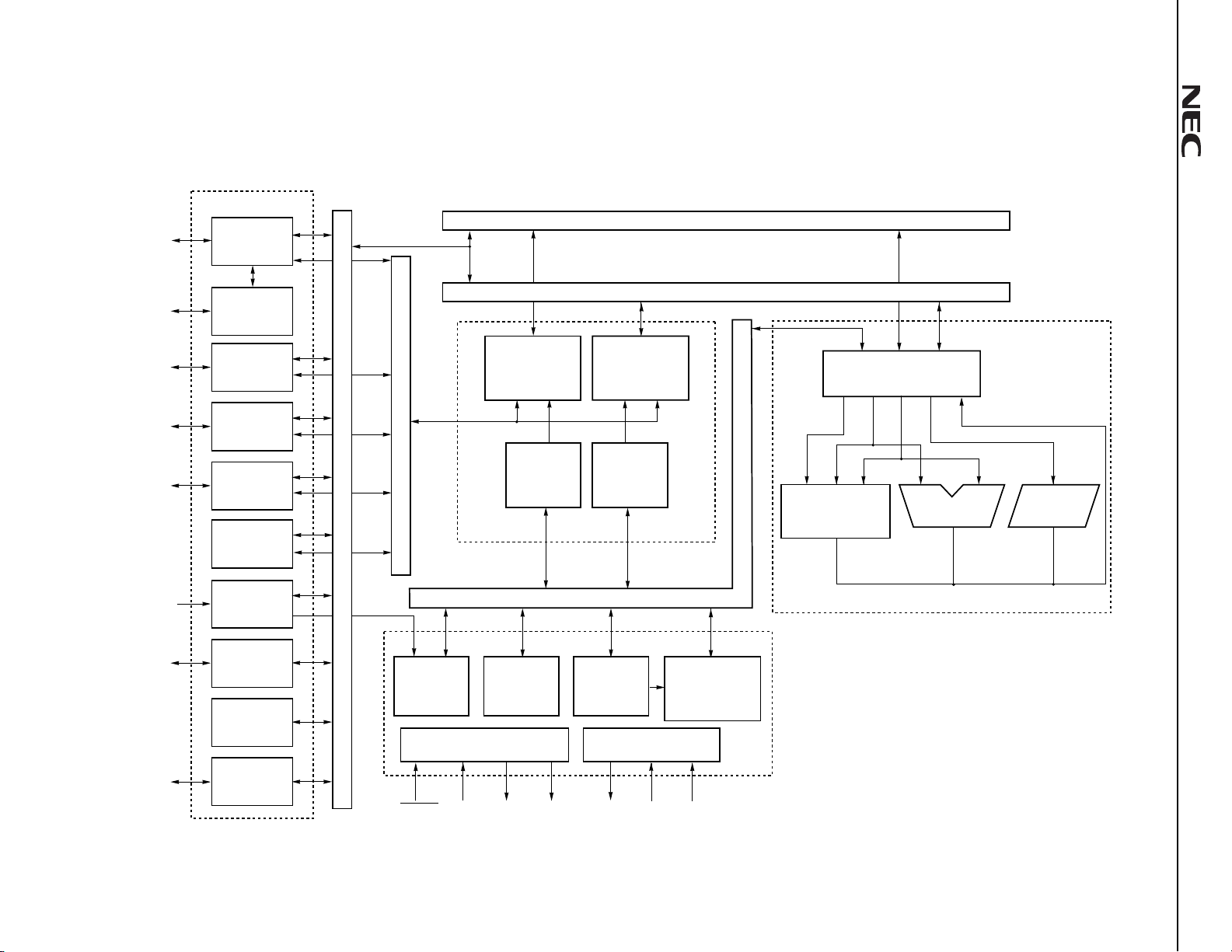
External memory
BLOCK DIAGRAM
Peripheral unit
X bus
External
memory I/O
unit
Y bus
Instruction
memory
MAC
16 × 16 + 40 → 40
R0 to R7
ALU (40)
Operation unit
BSFT
µµ
µ
µ
PD77210, 77213
Serial I/O
(AUDIO)
Serial I/O
(TDM)
Host I/O
DMA
controller
Interrupt
controller
Port
Timer
Note
Peripheral-memory transfer bus
Peripheral bus
Interrupt
control
Loop control
CPU control
X memory
X memory
data
addressing
unit
stack
Y memory
Y memory
data
addressing
unit
Data memory
Main bus
Program control
unit
PC stack
Clock control
SD Card I/O
Data Sheet U15203EJ3V0DS
IE
I/O
RESET
CSTOP
HALTS
STOPS
CLKOUT CLKIN
PLL
µ
Note PD77213 only
3
Page 4
FUNCTIONAL PIN BLOCK
Serial interface
(time division serial)
Serial interface
(audio serial)
SD card interface
Host interface
Note
Port
TSO
TSORQ
TSOEN
TSCK
TSI
TSIEN
TSIAK
ASOEN/LRCLK
ASIEN/MCLK
ASCK/BCLK
ASI
ASO
SDDAT0
SDCR
SDCLK
SDMON
P0 to P15
16
HCS
HA0, HA1
2
HRD
HRE
HWR
HWE
HD0 to HD15
16
+1.5 V +3.3 V
IV
DD
EV
DD
PLL0 to PLL3
MA0 to MA19
MD0 to MD15
TCK, TDI, TMS, TRST
RESET
INTmn
CLKIN
CLKOUT
STOPS
CSTOP
HALTS
MRD
MWR
MHOLDRQ
MHOLDAK
MBSTB
MWAIT
TIMOUT
TDO, TICE
µµµµ
PD77210, 77213
Reset and interrupt
16
Clock
4
System control
20
16
External data memory
interface
Timer
2
For debugging
4
GND
Note
PD77213 only
µ
Caution Some port pins, host interface pins, serial interface pins, interrupt pins, and SD card interface
pins are alternate function pins.
Remark m, n = 0 to 3
4
Data Sheet U15203EJ3V0DS
Page 5
DSP FUNCTION LIST
PD77115
µ
11.5 K × 32
16 K × 16 each
None
Integer multiple
of ×1 to 16
(external pin)
1 channel
(audio CODEC)
8 bits
1 channel
(16-bit resolution)
None
PD77114
µ
8 K × 16 each
Item
Memory
space
(words ×
bits)
Data Sheet U15203EJ3V0DS
Instruction cycle (at maximum
operating speed)
Multiple
Peripheral
Int. instruction RAM
Int. instruction ROM
Data RAM
(X/Y memory)
Data ROM
(X/Y memory)
Ext. instruction memory
Ext. data memory (X/Y
memory)
Serial interface
Host interface
General-purpose
port (I/O
programmable)
Timer
PD77110
µ
35.5 K × 32
None
24 K × 16 each
None
32 K × 16 each
15.3 ns
(65 MHz)
Integer multiple
of ×1 to 8
(external pin)
PD77111
µ
None
1 K × 32
31.75 K × 32
3 K × 16 each
16 K × 16 each
PD77112
µ
16 K × 16 each
Integer multiple of ×1 to 16
(mask option)
2 channels
(speech CODEC)
8-bit bus
4 bits
None
PD77113A
µ
None
13.3 ns
(75 MHz)
3.5 K × 32
48 K × 32
16 K × 16 each
32 K × 16 each
PD77210
µ
31.5 K × 32
None
30 K × 16 each
None
1 M × 16
6.25 ns
(160 MHz)
Integer multiple of ×10 to 64
(external pin)
2 channels (time-division, audio)
16-bit bus
16 bits (some are alternative with host)
2 channels
(16-bit resolution)
PD77213
µ
15.5 K × 32
64K × 32
18 K × 16 each
32 K × 16 each
1 M × 16 (8 K ×
16, using SD I/F)
8.33 ns
(120 MHz)
µµ
µ
µ
PD77210, 77213
SD card I/F
80-pin TQFP
80-pin FBGA
−
DSP core: 1.5 V
I/O pins: 3.3 V
161-pin FBGA
144-pin LQFP
SD card I/F
Supply voltage
Package
Others
−
100-pin TQFP
−
80-pin TQFP
80-pin FBGA
−
DSP core: 2.5 V
100-pin TQFP
I/O pins: 3 V
−
80-pin FBGA
−
100-pin TQFP
5
Page 6
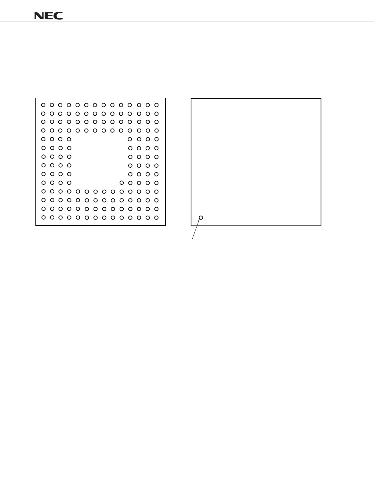
PIN CONFIGURATIONS
161-pin plastic fine pitch BGA (10 x 10)
•
µµµµ
PD77210F1-DA2
•
µµµµ
PD77213F1-xxx-DA2
(Bottom View) (Top View)
14
13
12
11
10
9
8
7
6
5
4
3
2
1
µµµµ
PD77210, 77213
MLK KLMPN PN
JHGFEDCBA ABCDEFGHJ
Index mark
6
Data Sheet U15203EJ3V0DS
Page 7
µµµµ
PD77210, 77213
Pin No. Pin Name Pin No. Pin Name Pin No. Pin Name Pin No. Pin Name
A1 NC C14 EV
DD
H2 HD7 M5 TSORQ
A2 NC D1 P10/HD10/INT22 H3 HD6 M6 MA0
A3 P5/INT11 D2 P11/HD11/INT32 H4 GND M7 MA4
A4 P2/INT20 D3 P12/HD12/INT03 H11 MD5 M8 MA5
A5 GND D4 GND H12 MD4 M9 MA10
A6 EV
A7 IV
A8 IV
DD
DD
DD
D5 GND H13 MD1 M10 MA12
D6 P1/INT10 H14 MD3 M11 MA15/Reserved
D7 GND J1 EV
DD
M12 MA19/SDCLK
A9 PLL0 D8 GND J2 HCS M13 MA18/SDCR
A10 STOPS D9 GND J3 HA1 M14 EV
A11 EV
DD
D10 GND J4 HWR N1 NC
DD
A12 TRST D11 TMS J11 GND N2 NC
A13 NC D12 TICE J12 MD0 N3 ASIEN/MCLK
A14 NC D13 MD12 J13 MBSTB N4 TSCK
B1 NC D14 MD15 J14 IV
DD
N5 TSIAK
B2 NC E1 P14/HD14/INT23 K1 HA0 N6 MA1
B3 P7/INT31 E2 P15/HD15/INT33 K2 HRD N7 MA2
B4 P6/INT21 E3 P13/HD13/INT13 K3 TIMOUT N8 MA7
B5 P3/INT30 E4 GND K4 ASO N9 MA9
B6 CLKOUT E5 NC K11 GND N10 MA11
B7 IV
DD
E11 GND K12 MWR N11 MA16/Reserved
B8 PLL3 E12 MD14 K13 MWAIT N12 MA17/Reserved
B9 PLL1 E13 MD9 K14 EV
DD
N13 NC
B10 CSTOP E14 MD11 L1 HWE N14 NC
B11 I.C. F1 EV
DD
L2 HRE P1 NC
B12 TCK F2 HD1 L3 GND P2 NC
B13 NC F3 HD2 L4 GND P3 ASI
B14 NC F4 HD0 L5 TSIEN P4 TSO
C1 EV
DD
C2 P8/HD8/INT02 F12 MD13 L7 GND P6 EV
C3 P9/HD9/INT12 F13 MD7 L8 MA8 P7 IV
C4 P4/INT01 F14 EV
C5 P0/INT00 G1 HD3 L10 MA14/SDDAT0
C6 CLKIN G2 HD5 L11 GND P10 EV
F11 MD10 L6 GND P5 TSI
DD
L9 GND P8 MA3
Note
P9 MA6
DD
DD
DD
C7 PLL2 G3 HD4 L12 MHOLDRQ P11 MA13/SDMON
C8 HALTS G4 GND L13 MRD P12 EV
DD
C9 RESET G11 GND L14 MHOLDAK P13 NC
C10 I.C. G12 MD8 M1 EV
DD
P14 NC
C11 TDI G13 MD2 M2 ASCK/BCLK
C12 TDO G14 MD6 M3 ASOEN/LRCLK
C13 GND H1 IV
Note MA13 to MA19 pins of the
PD77213 are alternate function pins.
µ
DD
M4 TSOEN
Note
Note
Note
Note
Note
Note
Data Sheet U15203EJ3V0DS
7
Page 8
144-pin plastic LQFP (fine pitch) (20 x 20) (Top View)
•
µµµµ
PD77210GJ-8EN
•
µµµµ
PD77213GJ-xxx-8EN
Note
µµµµ
PD77210, 77213
Note
GND
TCK
TDI
TMS
TRST
I.C.
I.C.
EV
GND
RESET
STOPS
CSTOP
HALTS
PLL0
PLL1
PLL2
PLL3
IV
GND
CLKIN
IV
GND
IV
GND
CLKOUT
EV
GND
P0/INT00
P1/INT10
P2/INT20
P3/INT30
P4/INT01
P5/INT11
P6/INT21
P7/INT31
GND
DD
TDO
TICE
GND
EV
144 120121122123124125126127128129130131
1
2
3
4
5
6
DD
DD
DD
DD
DD
7
8
9
10
11
12
13
14
15
16
17
18
19
20
21
22
23
24
25
26
27
28
29
30
31
32
33
34
35
36
MD15
MD14
MD12
MD13
MD11
MD10
134135136137138139140141142143
GND
DD
EV
MD4
MD5
MD2
MD3
MD6
MD7
MD8
MD9
132133
GND
DD
DD
GND
EV
MBSTB
MWAIT
MD0
MD1
IV
5958575655545352515049484746454443424140393837
6160
MWR
MRD
MHOLDAK
676665646362
MA18/SDCR
MA19/SDCLK
MHOLDRQ
71706968
DD
EV
GND
109110111112113114115116117118119
108
107
106
105
104
103
102
101
100
99
98
97
96
95
94
93
92
91
90
89
88
87
86
85
84
83
82
81
80
79
78
77
76
75
74
73
72
EV
DD
MA17/Reserved
MA16/Reserved
MA15/Reserved
MA14/SDDAT0
MA13/SDMON
MA12
MA11
MA10
GND
EV
DD
MA9
MA8
MA7
MA6
MA5
MA4
MA3
MA2
GND
IV
DD
GND
EV
DD
MA1
MA0
TSIAK
TSORQ
TSI
TSIEN
TSCK
TSO
TSOEN
ASI
ASIEN/MCLK
ASCK/BCLK
GND
Note
Note
Note
Note
Note
DD
GND
EV
P8/HD8/INT02
P9/HD9/INT12
P10/HD10/INT22
P11/HD11/INT32
Note MA13 to MA19 pins of the
8
DD
EV
P12/HD12/INT03
P13/HD13/INT13
P14/HD14/INT23
P15/HD15/INT33
PD77213 are alternate function pins.
µ
HD5
HD4
HD3
HD2
HD1
HD0
GND
Data Sheet U15203EJ3V0DS
HD6
HD7
DD
DD
IV
GND
EV
GND
HCS
HA0
HA1
HRD
HRE
HWR
HWE
DD
ASO
EV
TIMOUT
ASOEN/LRCLK
GND
Page 9
µµµµ
PD77210, 77213
Pin No
.
1GND 37EV
2 TCK 38 GND 74 ASCK/BCLK 110 EV
Pin Name Pin No
.
Pin Name Pin No
DD
.
Pin Name Pin No
.
73 GND 109 GND
Pin Name
DD
3 TDI 39 P8/HD8/INT02 75 ASIEN/MCLK 111 MA18/SDCR
4 TMS 40 P9/HD9/INT12 76 ASI 112 MA19/SDCLK
5 TRST 41 P10/HD10/INT22 77 TSOEN 113 MHOLDRQ
6 I.C. 42 P11/HD11/INT32 78 TSO 114 MHOLDAK
7 I.C. 43 P12/HD12/INT03 79 TSCK 115 MRD
8EV
DD
44 P13/HD13/INT13 80 TSIEN 116 MWR
9 GND 45 P14/HD14/INT23 81 TSI 117 MWAIT
10 RESET 46 P15/HD15/INT33 82 TSORQ 118 MBSTB
11 STOPS 47 EV
DD
83 TSIAK 119 MD0
12 CSTOP 48 GND 84 MA0 120 MD1
13 HALTS 49 HD0 85 MA1 121 EV
14 PLL0 50 HD1 86 EV
DD
122 GND
15 PLL1 51 HD2 87 GND 123 IV
16 PLL2 52 HD3 88 IV
DD
124 GND
DD
DD
17 PLL3 53 HD4 89 GND 125 MD2
18 IV
DD
54 HD5 90 MA2 126 MD3
19 GND 55 HD6 91 MA3 127 MD4
20 CLKIN 56 HD7 92 MA4 128 MD5
21 IV
DD
57 IV
DD
93 MA5 129 MD6
22 GND 58 GND 94 MA6 130 MD7
23 IV
DD
59 EV
DD
95 MA7 131 MD8
24 GND 60 GND 96 MA8 132 MD9
25 CLKOUT 61 HCS 97 MA9 133 EV
26 EV
DD
62 HA0 98 EV
DD
134 GND
DD
27 GND 63 HA1 99 GND 135 MD10
28 P0/INT00 64 HRD 100 MA10 136 MD11
29 P1/INT10 65 HRE 101 MA11 137 MD12
30 P2/INT20 66 HWR 102 MA12 138 MD13
31 P3/INT30 67 HWE 103 MA13/SDMON
32 P4/INT01 68 TIMOUT 104 MA14/SDDAT0
33 P5/INT11 69 ASOEN/LRCLK 105 MA15/Reserved
34 P6/INT21 70 ASO 106 MA16/Reserved
35 P7/INT31 71 EV
DD
36 GND 72 GND 108 EV
Note MA13 to MA19 pins of the
PD77213 are alternate function pins.
µ
107 MA17/Reserved
DD
Note
Note
Note
Note
Note
139 MD14
140 MD15
141 TDO
142 TICE
143 GND
144 EV
DD
Note
Note
Data Sheet U15203EJ3V0DS
9
Page 10

Pin Name
µµµµ
PD77210, 77213
ASCK :Audio Serial Clock Input/Output
ASI :Audio Serial Data Input
ASIEN :Audio Serial Input Enable
ASO :Audio Serial Data Output
ASOEN :Audio Serial Output Enable
BCLK :Bit Clock Input/Output
CLKIN :Clock Input
CLKOUT :Clock Output
CSTOP :Clear Stop Mode
EV
DD
GND :Ground
HALTS :Halt Status Signal Output
HD0 to HD15 :Host Data Bus
HCS :Host Chip Select
HA0, HA1 :Host Data Access
HRD :Host Read
HRE :Host Read Enable
HWE :Host Write Enable
HWR :Host Write
I.C. :Internal Connection
IV
DD
INTmn :Interrupt (m,n=0 to 3)
LRCLK :Left Right Clock Input/Output
MA0 to MA19 :External Data Memory Address Bus
MBSTB :External Data Memory Bus Strobe
MCLK :Master Clock Input
MD0 to MD15 :External Data Memory Bus
MHOLDAK :External Data Memory Bus Hold
MHOLDRQ :External Data Memory Bus Hold
MRD :External Data Memory Read Output
MWR :External Data Memory Write Output
:Power Supply for I/O Pins
:Power Supply for DSP Core
Acknowledge
Request
MWAIT :External Data Memory Access Wait
Input
NC :Non-Connection
P0 to P15 :Port
PLL0-PLL3 :PLL Multiple Rate Set
Reserved :Reserved
RESET :Reset
SDCLK :SD Card Clock Output
SDCR :SD Card Command Output/Response
Input
SDDAT0 :SD Card Data Input/Output
SDMON :SD Card Access Monitor
STOPS :Stop Status Signal Output
TCK :Test Clock Input
TDI :Test Data Input
TDO :Test Data Output
TICE :Test In-Circuit Emulator
TIMOUT :Timer Time Out Monitor Output
TMS :Test Mode Select
TRST :Test Reset
TSCK :Time Division Multiplex Serial Clock
Input
TSI :Time Division Multiplex Serial Data Input
TSIAK :Time Division Multiplex Serial Input
Acknowledge
TSIEN :Time Division Multiplex Serial Input
Enable
TSO :Time Division Multiplex Serial Data
Output
TSOEN :Time Division Multiplex Serial Output
Enable
TSORQ :Time Division Multiplex Serial Output
Request
10
Data Sheet U15203EJ3V0DS
Page 11

µµµµ
PD77210, 77213
CONTENTS
1. PIN FUNCTIONS....................................................................................................................................13
1.1 Description of Pin Functions ........................................................................................................................13
1.2 Connection of Unused Pins ..........................................................................................................................21
1.2.1 Connection of functional pins ..................................................................................................................21
1.2.2 Connection of non-functional pin.............................................................................................................22
2. FUNCTIONAL OUTLINE .......................................................................................................................23
2.1 Program Control Unit.....................................................................................................................................23
2.1.1 CPU control .............................................................................................................................................23
2.1.2 Interrupt control .......................................................................................................................................23
2.1.3 Loop control stack ...................................................................................................................................23
2.1.4 PC stack ..................................................................................................................................................23
2.1.5 Clock control............................................................................................................................................23
2.1.6 Instruction memory ..................................................................................................................................24
2.2 Operation Unit ................................................................................................................................................24
2.2.1 General-purpose registers (R0 to R7) .....................................................................................................24
2.2.2 Multiply accumulator (MAC) ....................................................................................................................24
2.2.3 Arithmetic logic unit (ALU) .......................................................................................................................24
2.2.4 Barrel shifter (BSFT)................................................................................................................................24
2.3 Data Memory Unit...........................................................................................................................................24
2.3.1 Data memory ...........................................................................................................................................24
2.3.2 Data addressing unit................................................................................................................................25
2.4 Peripheral Unit................................................................................................................................................25
2.4.1 Serial interface (SIO) ...............................................................................................................................25
2.4.2 Host interface (HIO).................................................................................................................................25
2.4.3 General-purpose I/O port (PIO) ...............................................................................................................26
2.4.4 External memory interface (MIO).............................................................................................................26
2.4.5 Timers (TIM1 and TIM2)..........................................................................................................................26
2.4.6 Interrupt controller (INTC)........................................................................................................................26
2.4.7 DMA controller (PMT)..............................................................................................................................26
2.4.8 SD card interface (SDCIF).......................................................................................................................26
2.4.9 Debug interface (IEIO).............................................................................................................................26
3. CLOCK GENERATOR...........................................................................................................................27
4. RESET FUNCTION ................................................................................................................................28
4.1 Hardware Reset ..............................................................................................................................................28
5. FUNCTION OF BOOT-UP ROM ...........................................................................................................28
5.1 Boot at Reset ..................................................................................................................................................28
5.1.1 Memory boot............................................................................................................................................28
5.1.2 Host boot .................................................................................................................................................29
5.1.3 Serial boot ...............................................................................................................................................29
5.2 Reboot.............................................................................................................................................................29
5.2.1 Memory reboot ........................................................................................................................................29
Data Sheet U15203EJ3V0DS
11
Page 12

µµµµ
PD77210, 77213
5.2.2 Host reboot ............................................................................................................................................. 30
5.2.3 Serial reboot ........................................................................................................................................... 30
6. STANDBY MODE.................................................................................................................................. 31
6.1 Halt Mode ....................................................................................................................................................... 31
6.2 Stop Mode ...................................................................................................................................................... 31
7. MEMORY MAP...................................................................................................................................... 32
7.1 Instruction Memory ....................................................................................................................................... 32
7.1.1 Instruction memory map ......................................................................................................................... 32
7.1.2 Interrupt vector table............................................................................................................................... 33
7.2 Data Memory.................................................................................................................................................. 34
7.2.1 Data memory map .................................................................................................................................. 34
7.2.2 Internal peripherals ................................................................................................................................. 35
8. GENERAL-PURPOSE PORT AND INTERRUPT ............................................................................... 38
8.1 General-purpose Port Pins ........................................................................................................................... 38
8.2 Interrupt Pin ................................................................................................................................................... 38
9. INSTRUCTION ....................................................................................................................................... 39
9.1 Outline of Instruction .................................................................................................................................... 39
9.2 Instruction Set and Its Operation................................................................................................................. 40
10. ELECTRICAL SPECIFICATIONS....................................................................................................... 46
11. PACKAGE DRAWINGS...................................................................................................................... 69
12. RECOMMENDED SOLDERING CONDITIONS................................................................................. 71
12
Data Sheet U15203EJ3V0DS
Page 13
µµµµ
PD77210, 77213
1. PIN FUNCTIONS
Because the pin numbers differ depending on the package, see the column for the package to be used in the
tables below.
1.1 Description of Pin Functions
•••• Power supply pins
Pin No.Pin Name
144-pin LQFP 161-pin FBGA
IV
DD
EV
DD
GND 1,9,19,22,24,
18,21,23,57,
88,123
8,26,37,47,59,
71,86,98,108,
110,121,133,
144
27,36,38,48,
58,60,72,73,
87,89,99,109,
122,124,134,
143
A7,A8,B7,H1,
J14, P7
A6,A11,C1,
C14,F1,F14,
J1,K14,M1,
M14,P6,P10,
P12
A5,C13,D4,D5,
D7,D8,D9,D10,
E4,E11,G4,
G11,H4,J11,
K11,L3,L4,L6,
L7,L9,L11
Remark Please supply voltage to the IV
I/O Function Alternate
− Power supply for DSP core (+1.5 V)
These pins supply power to the DSP core.
− Power supply for I/O (+3.3 V)
These pins supply power to the external interface
pins.
− Ground
These are ground pins.
DD
and EVDD pins simultaneously.
Pin
−
−
−
Data Sheet U15203EJ3V0DS
13
Page 14
•••• Clock and system control pins
Pin No.Pin Name
144-pin LQFP 161-pin FBGA
CLKIN 20 C6 Input Clock input
CLKOUT 25 B6 Output Internal system clock output
PLL0 to
PLL3
HALTS 13 C8 Output HALT mode status output
STOPS 11 A10 Output Stop mode status output
CSTOP 12 B10 Input Stop mode clear signal input
14 to 17 A9,B9,C7,B8 Input PLL multiple setting input
I/O Function Alternate
This pin inputs a clock to operate the
Family.
This pin outputs the internal system clock that is the
clock input from CLKIN and which is multiplied by the
PLL circuit.
These pins set a clock multiple of the PLL circuit.
• PLL3: PLL2: PLL1: PLL0
0000: x10 0001: x12 0010: x14
0011: x16 0100: x18 0101: x20
0110: x22 0111: x24 1000: x26
1001: x28 1010: x30 1011: x32
1100: x40 1101: x48 1110: x56
1111: x64
This pin is asserted active in halt mode and stop
mode.
This pin is asserted active in stop mode.
Stop mode is cleared when this pin is asserted
active.
µµµµ
PD77210, 77213
PD77210
µ
Pin
−
−
−
−
−
−
14
Data Sheet U15203EJ3V0DS
Page 15
µµµµ
PD77210, 77213
•••• Reset and interrupt pins
Pin No.Pin Name
144-pin LQFP 161-pin FBGA
RESET 10 C9 Input Internal system reset signal input
INT00 28 C5 Input P0
INT01 32 C4 Input P4
INT02 39 C2 Input P8/HD8
INT03 43 D3 Input P12/HD12
INT10 29 D6 Input P1
INT11 33 A3 Input P5
INT12 40 C3 Input P9/HD9
INT13 44 E3 Input P13/HD13
INT20 30 A4 Input P2
INT21 34 B4 Input P6
INT22 41 D1 Input P10/HD10
INT23 45 E1 Input P14/HD14
INT30 31 B5 Input P3
INT31 35 B3 Input P7
INT32 42 D2 Input P11/HD11
INT33 46 E2 Input
I/O Function Alternate
Pin
−
This pin initializes the
Maskable external interrupt input
These pins input external interrupts.
PD77210 Family.
µ
P15/HD15
Data Sheet U15203EJ3V0DS
15
Page 16
•••• External data memory interface
Pin No.Pin Name
144-pin LQFP 161-pin FBGA
MA0 to
MA19
MD0 to
MD15
MWR 116 K12 Output
MRD 115 L13 Output
MHOLDAK 114 L14 Output Hold acknowledge signal
MHOLDRQ 113 L12 Input Hold request signal
MWAIT 117 K13 Input Wait signal input
MBSTB 118 J13 Output Bus strobe signal
Note
84, 85,
90 to 97,
100 to 107,
111, 112
119,120,
125 to 132,
135 to 140
M6,N6,N7,P8,
M7,M8,P9,N8,
L8,N9,M9,N10,
M10,P11,L10,
M11,N11,N12,
M13,M12
J12,H13,G13,
H14,H12,H11,
G14,F13,G12,
E13,F11,E14,
D13,F12,E12,
D14
I/O Function Alternate
Output
(3S)
I/O
(3S)
(3S)
(3S)
Address bus of external data memory
These pins output an address when the external data
memory is accessed.
16-bit data bus
These pins input/output data when the external data
memory is accessed.
Write output
This pin outputs a write strobe signal for the external
data memory.
Read output
This pin outputs a read strobe signal for the external
data memory.
This pin goes low when the external device is
granted use of the external data memory bus of the
PD77210 Family.
µ
The external device inputs a low level to this pin
when it uses the external data memory bus of the
PD77210 Family.
µ
This pin inserts wait cycles when the
Family accesses the external data memory.
• 0: Inserts wait cycles.
• 1: Does not insert wait cycles.
This pin goes low while the
the external data memory bus.
Note MA13 to MA19 pins of the µPD77213 are alternate function pins.
µµµµ
PD77210, 77213
PD77210
µ
PD77210 Family uses
µ
Pin
SDCLK,
SDCR,
SDDAT0,
SDMON
−
−
−
−
−
−
−
Remark Those pins marked “3S” in the above table enter the high-impedance state under the following
conditions:
MA0 to MA19, MRD, and MWR: When the bus is released (MHOLDAK = low level)
MD0 to MD15: When the external data memory is not accessed and when the bus is released
(MHOLDAK = low level)
16
Data Sheet U15203EJ3V0DS
Page 17
µµµµ
PD77210, 77213
•••• Timer
Pin No.Pin Name
144-pin LQFP 161-pin FBGA
TIMOUT 68 K3 Output Time out monitor
I/O Function Alternate
Pin
This pin is asserted active when the timer times out.
•••• Serial interface
Pin No.Pin Name
144-pin LQFP 161-pin FBGA
ASCK/
BCLK
ASO 70 K4 Output
ASI 76 P3 Input Audio serial data input −
ASOEN/
LRCLK
ASIEN/
MCLK
TSCK 79 N4 Input Clock input for time division serial −
TSO 78 P4 Output
TSI 81 P5 Input Time-division serial data input −
TSORQ 82 M5 Output Time-division serial output request −
TSOEN 77 M4 Input Time-division serial output enable −
TSIEN 80 L5 Input Time-division serial input enable −
TSIAK 83 N5 Output Time-division serial input acknowledge −
74 M2 I/O Audio serial clock input/output
69 M3 I/O Audio serial output enable/left right clock input output
75 N3 Input Audio serial input enable/master clock input output
I/O Function Alternate
Pin
ASCK:Audio serial clock input
BCLK:Serial clock I/O
Audio serial data output −
(3S)
ASOEN:Audio serial output enable input
LRCLK:Left right clock I/O
ASIEN:Audio serial input enable input
MCLK:Master clock input (in master mode)
Time-division serial data output −
(3S)
Remark Those pins marked “3S” in the above table enter the high-impedance state when data transmission is
completed and when the hardware reset (RESET) signal is input.
−
−
−
−
Data Sheet U15203EJ3V0DS
17
Page 18
µµµµ
PD77210, 77213
•••• Host interface
Pin No.Pin Name
144-pin LQFP 161-pin FBGA
HA1 63 J3 Input Host address 1
HA0 62 K1 Input Host address 0
HCS 61 J2 Input Chip select input −
HRD 64 K2 Input Host read input −
HWR 66 J4 Input Host write input −
HRE 65 L2 Output Host read enable output −
HWE 67 L1 Output Host write enable output −
HD0 to
HD7
HD8 to
HD15
49 to 56 F4,F2,F3,G1,
G3,G2,H3,H2
39 to 46 C2,C3,D1,D2,
D3,E3,E1,E2
I/O Function Alternate
Pin
This pin specifies a register that is accessed by the
host interface pins (HD7 to HD0, or HD15 to HD0).
• 1: The host interface status register (HST) is
accessed.
• 0: The host transmit data register (HDT (out)) is
accessed for read (HRD = 0) and the host receive
data register (HDT (in)) is accessed for write (HWR
= 0).
This pin specifies a register that is accessed by HD7
to HD0 in 8-bit mode. This pin is invalid in 16-bit
mode.
• 1: Bits 15 to 8 of HST, HDT (in), and HDT (out) are
accessed.
• 0: Bits 7 to 0 of HST, HDT (in), and HDT (out)
are accessed.
I/O
(3S)
I/O
(3S)
8-bit host data bus
These pins constitute a host data bus in 8-bit host
mode. Access to 16-bit data for input/output is
controlled by the HA0 pin, and the data is accessed
two times such that it is divided into two blocks of 8-
bit data.
In 16-bit mode, the lower 8 bits of the data are
input/output.
Host data bus
These pins constitute a host data bus in 16-bit host
mode. They input/output 16-bit data with HD0 to
HD7.
P8 to P15/
INT02,
INT12,
INT22,
INT32,
INT03,
INT13,
INT23,
INT33
Remark Those pins marked “3S” in the above table enter the high-impedance state while the host interface is not
being accessed.
−
−
−
18
Data Sheet U15203EJ3V0DS
Page 19
µµµµ
PD77210, 77213
•••• I/O port
Pin No.Pin Name
144-pin LQFP 161-pin FBGA
P0 28 C5 I/O INT00
P1 29 D6 I/O INT10
P2 30 A4 I/O INT20
P3 31 B5 I/O INT30
P4 32 C4 I/O INT01
P5 33 A3 I/O INT11
P6 34 B4 I/O INT21
P7 35 B3 I/O INT31
P8 39 C2 I/O INT02/HD8
P9 40 C3 I/O INT12/HD9
P10 41 D1 I/O INT22/HD10
P11 42 D2 I/O INT32/HD11
P12 43 D3 I/O INT03/HD12
P13 44 E3 I/O INT13/HD13
P14 45 E1 I/O INT23/HD14
P15 46 E2 I/O
I/O Function Alternate
Pin
General-purpose I/O port
INT33/HD15
•••• Debugging interface
Pin No.Pin Name
144-pin LQFP 161-pin FBGA
TDO 141 C12 Output
TICE 142 D12 Output −
TCK 2 B12 Input −
TDI 3 C11 Input −
TMS 4 D11 Input −
TRST 5 A12 Input
I/O Function Alternate
Pin
For debugging
(3S)
This interface pins are used when a debugger is
used.
Remark Those pins marked “3S” in the above table enter the high-impedance state while the debugging interface
is not being accessed.
−
−
Data Sheet U15203EJ3V0DS
19
Page 20
µµµµ
PD77210, 77213
••••SD card interface (
SDCLK 112 M12 Output SD card clock output
SDCR 111 M13 I/O
SDDAT0 104 L10 I/O
SDMON 103 P11 Output SD card interface access monitor
Reserved 105 to 107 M11, N11, N12 − Reserved for future function expansion.
µµµµ
PD77213 only)
Pin No.Pin Name
144-pin LQFP 161-pin FBGA
I/O Function Alternate
Pin
MA19
• Leave this pin open.
(3S)
(3S)
SD cord command/response
Input: Response
Output: Command
• Leave pull-up.
SD card data input/output
Input: Read data
Output: Write data
• Leave pull-up.
This pin outputs a high level when the SD card
interface is being accessed.
1: SD card interface being accessed
0: SD card interface not being accessed
This pin becomes high impedance when the SD card
interface is being used.
MA18
MA14
MA13
MA15 to
MA17
Remark Those pins marked “3S” in the above table enter the high-impedance state when the SD card interface is
not being accessed.
•••• Others
Pin No.Pin Name
144-pin LQFP 161-pin FBGA
I.C. 6, 7 B11, C10 − Internally connected.
NC − A1,A2,A13,
A14,B1,B2,
B13,B14,E5,
N1,N2,N13,
N14,P1,P2,
P13,P14
I/O Function Alternate
Leave these pins open.
− No connection.
Leave these pins open.
Caution If any signal is input to these pins or if these pins are read, the correct operation of the
Family is not guaranteed.
Pin
−
−
µµµµ
PD77210
20
Data Sheet U15203EJ3V0DS
Page 21
µµµµ
PD77210, 77213
1.2 Connection of Unused Pins
1.2.1 Connection of functional pins
Connect the unused pins as shown in the table below.
Pin Name I/O Recommended Connection
STOPS, HALTS Output Leave open.
CSTOP Input Connect to GND via a pull-down resistor.
CLKOUT Output Leave open.
P0 to P15 I/O Connect to EVDD via a pull-up resistor or to GND via a pull-down resistor.
HD0 to HD7
HA0, HA1 Input Connect to EVDD via a pull-up resistor or to GND via a pull-down resistor.
HCS, HRD, HWR Input Connect to EV
HRE, HWE Output Leave open.
TIMOUT Output Leave open.
ASCK, TSCK Input
ASI, TSI Input
ASIEN, TSIEN Input
ASOEN, TSOEN,
LRCLK
ASO, TSO Output
TSORQ Output
TSIAK Output
MA0 to MA19 Output Leave open.
MD0 to MD15
MRD, MWR Output Leave open.
MHOLDRQ Input Connect to EVDD via a pull-up resistor.
MBSTB, MHOLDAK Output Leave open.
MWAIT Input Connect to EVDD via a pull-up resistor.
TCK Input Connect to GND via a pull-down resistor.
TDO, TICE Output Leave open.
TMS, TDI Input Leave open (this pin is internally pulled up).
TRST Input Leave open (this pin is internally pulled down).
Note 1
Note 2
I/O Connect to EVDD via a pull-up resistor or to GND via a pull-down resistor.
via a pull-up resistor.
DD
Connect to EVDD
Connect to GND via a pull-down resistor.
Input
Leave open.
I/O Connect to EVDD via a pull-up resistor or to GND via a pull-down resistor.
via a pull-up resistor or to GND via a pull-down resistor.
Notes 1. These pins may left opened if the HCS, HRD,and HWR are fixed to the high level.
However, connect these pins as recommended in the HALT and STOP modes when the power
consumption must be lowered.
2. These pins may leave opened if the external data memory is not accessed in the program.
However, connect these pins as recommended in the HALT and STOP modes when the power
consumption must be lowered.
Caution Unused alternate-function pins should be handled in accordance with the processing specified
for the pin function of the initial setting.
Data Sheet U15203EJ3V0DS
21
Page 22
1.2.2 Connection of non-functional pin
Pin name I/O Recommended Connection
I.C. − Leave open.
NC − Leave open.
µµµµ
PD77210, 77213
22
Data Sheet U15203EJ3V0DS
Page 23

2. FUNCTIONAL OUTLINE
2.1 Program Control Unit
µµµµ
PD77210, 77213
This unit controls the execution of
interrupts, clock, and standby mode.
2.1.1 CPU control
A three-stage pipeline architecture is employed so that all instructions, except branch instructions and some
others, can be executed with one system clock.
2.1.2 Interrupt control
The interrupt control circuit services the interrupt requests input to the interrupt controller by an external pin
(INTmn) or internal peripherals (such as the serial interface, host interface, timer, and DMA controller). The interrupt
of each interrupt source can be individually enabled or disabled. In addition, multiple interrupts are also supported.
2.1.3 Loop control stack
A loop function without any hardware overhead is realized. A 4-level loop stack is provided to support multiple
loops.
2.1.4 PC stack
A 15-level PC stack that stacks the program counter supports multiple interrupts/subroutine calls.
2.1.5 Clock control
A PLL and a divider are internally provided as a clock generator so that an externally input clock is multiplied or
divided and supplied as the operating clock to the µPD77210 Family. The multiple of the PLL can be set by using
external pins (PLL0 to PLL3) within a range of ×10 to 64. The division ratio can be set by using a register in a range
of ÷1 to 16.
The clock control register (CLKC) controls the power (ON/OFF) to the PLL, selects a clock source, controls the
output divider, and controls the output of the CLKOUT pin.
Two types of standby modes are available so that the power consumption can be reduced when the µPD77210
Family is standing by.
PD77210 Family by executing instructions and controlling branching, loop,
µ
•HALT mode: Current consumption falls to several mA upon execution of the HALT instruction.
This mode is released by an interrupt or hardware reset.
•STOP mode:Current consumption falls to hundreds of
This mode is released by hardware reset or inputting a signal to CSTOP pin.
Note When the PLL is stopped
Data Sheet U15203EJ3V0DS
Note
A
upon execution of the STOP instruction.
µ
23
Page 24

µµµµ
PD77210, 77213
2.1.6 Instruction memory
Of the instruction RAM, 64 words are allocated as interrupt vectors.
PD77210 is provided with an instruction RAM of 31.5 Kwords. The µPD77213 is provided with an instruction
The
µ
RAM of 15.5 Kwords and instruction ROM of 64 Kwords.
A boot-up ROM that boots up the instruction RAM is also provided, and the instruction RAM can be initialized or
rewritten by means of a memory boot (booting from an internal or external data space), host boot (booting via a host
interface), or serial boot (booting via a serial interface).
2.2 Operation Unit
This unit performs multiplication, addition, logic, and shift operations, and consists of a 40-bit multiply
accumulator, a 40-bit data ALU, a 40-bit barrel shifter, and eight 40-bit general-purpose registers.
2.2.1 General-purpose registers (R0 to R7)
These eight 40-bit registers input/output operands and load/store data to/from data memory.
Each register consists of three parts: R0L to R7L (bits 15 to 0), R0H to R7H (bits 31 to 16), and R0E to R7E (bits
39 to 32). Depending on the type of the operation, RnL, RnH, and RnE are used either as one register or in
combination.
2.2.2 Multiply accumulator (MAC)
The multiply accumulator performs multiplication of two 16-bit data items and addition or subtraction between the
result of the multiplication and one 40-bit data item, and then outputs 40-bit data.
A shifter (MSFT: MAC shifter) is provided at the preceding stage of the MAC, so that the 40-bit data that is to be
added to or subtracted from the multiplication result can be arithmetically shifted 1 bit or 16 bits to the right before
addition or subtraction.
2.2.3 Arithmetic logic unit (ALU)
The ALU accepts one or two 40-bit data items as input, performs an arithmetic or logical operation, and then
outputs 40-bit data.
2.2.4 Barrel shifter (BSFT)
The BFST accepts 40-bit data items as input, shifts the data to the left or right by an arbitrary number of bits, and
then outputs 40-bit data. The data can be shifted to the right arithmetically, in which case the sign of the data is
extended, or logically in which case 0 is inserted starting from the MSB.
2.3 Data Memory Unit
The data memory unit consists of two planes of data memory spaces and two pairs of data addressing units.
2.3.1 Data memory
Two data memory planes (X data memory and Y data memory) are provided. The data memory space includes a
64-word peripheral area.
The µPD77210 has a data RAM consisting of 30 Kwords × 2 planes. The µPD77213 has a data RAM consisting
of 18 Kwords × 2 planes, and has a data ROM consisting of 32 Kwords × 2 planes.
In addition, They also have an external data memory interface that is used to connect an external 1 Mword data
memory to the device.
24
Data Sheet U15203EJ3V0DS
Page 25

µµµµ
PD77210, 77213
2.3.2 Data addressing unit
An independent data addressing unit is provided for each of the X and Y data memory spaces.
Each data addressing unit has four data pointers (DPn), four index registers (DNn), one module register (DMX or
DMY), and an address ALU.
2.4 Peripheral Unit
The peripheral unit has serial interfaces, a host interface, general-purpose I/O ports, timers, an external memory
interface, and SD card interface (
memory spaces and are accessed as memory-mapped I/Os by the program.
2.4.1 Serial interface (SIO)
Two serial interface channels, an audio serial interface (ASIO) and a time-division serial interface (TDMSIO), are
provided.
The audio serial interface can be used in either of two modes: audio mode and standard mode. The standard
mode is compatible with the existing µPD77111 Family. The audio mode is compatible with the µPD77115.
The features of the audio mode are as follows:
PD77213 only). All these internal peripherals are mapped to the X and Y data
µ
• Mode: Master mode and slave mode
Master mode: Supports master clock input (MCLK), bit clock output (BCLK), LR clock output (LRCLK), 256 fs,
384 fs, and 512 fs.
Slave mode: Bit clock input (BCLK) and LR clock input (LRCLK)
• Frame format: 32- or 64-bit audio formats (LRCLK format)
• Handshake: Handshaking with external devices by a dedicated frame signal (LRCLK) and with the internal
circuitry by polling, wait, or interrupt
The standard mode has the following features:
•Serial clock: Supplied from an external source to each channel. The clock is shared for input and output by
each channel.
•Frame length: 8 or 16 bits, with MSB or LSB first selected for each channel.
•Handshake: Handshaking with the external device by using a dedicated status signal and with the internal
circuitry by polling, wait, or interrupt.
The time-division serial interface divides the serial input/output signal into 1 to 32 time slots and allows several
devices to share the serial bus. Because the T1 and E1 frame signals are considered. The time slot can be extended
from 1 to 128.
2.4.2 Host interface (HIO)
This is a parallel port that inputs/outputs data from/to an external host CPU and DMA controller. It can be used in
either 8-bit parallel mode or 16-bit parallel mode. In the µPD77210 Family, 16-bit registers are mapped to memory
for input data, output data, and status. Handshaking with an external device is performed by using a dedicated
status signal, and the internal circuitry handshaking is done by means of polling, wait, or interrupts.
The 8-bit parallel mode is compatible with the existing members of the µPD77111 Family.
In 16-bit parallel mode, some port pins are used as host interface pins.
Data Sheet U15203EJ3V0DS
25
Page 26

µµµµ
PD77210, 77213
2.4.3 General-purpose I/O port (PIO)
This is a 16-bit I/O port that can be set to either input or output mode in 1-bit units.
The external pins alternate between interrupt pins and host interface pins. By setting the mode of 8 bits of the
port to host interface pin mode, the host interface can be set in the 16-bit parallel mode.
2.4.4 External memory interface (MIO)
This interface accesses an external 1 Mwords data memory area in either of two modes: direct access and DMA
access modes. In DMA access mode, access is made via a memory-mapped register.
In direct access mode, the data paging register (DPR) is set to 0x3F and a page area is accessed as an access
window. An address of the external memory consists of 20 bits with the 8-bit value of the index register added as bits
12 to 19.
In DMA access mode, the address is automatically updated when a memory-mapped register is accessed. The
address is updated in an increment addressing mode in which the address is simply incremented, or in two-
dimensional addressing mode in which an offset is added to each line length.
The number of wait cycles to be inserted when the external memory is accessed can be specified by a register
(MWAIT), within a range of 1 to 15. In addition, wait cycles can also be inserted by using the MWAIT pin.
2.4.5 Timers (TIM1 and TIM2)
PD77210 Family has two timer channels.
The
µ
These timers can be used as interval timers, event counters, watchdog timers, and free-run timers.
The clock input to the timers is selected from the system clock, serial clock (ASCK or TSCK), external interrupt
(INT00, INT10, INT20, or INT30), or output of each timer.
The count value is 16 bits and the clock input by the prescaler can be divided by 1, 2, 4, 8, 16, 32, 64, or 128.
2.4.6 Interrupt controller (INTC)
The interrupt controller has functions for selecting and masking interrupt signals. It controls the interrupt signal to
be input to the DSP core.
2.4.7 DMA controller (PMT)
The DMA controller realizes data transfer between the peripherals and memory (peripheral-memory transfer) in
the background. It mitigates the software overhead generated by interrupt processing of the data input/output via
SIO, HIO, MIO, and SDCIF (µPD77213 only).
Data of 14 Kwords at addresses 0x0000 to 0x37FF of the internal data RAM can be transferred by means of
DMA.
2.4.8 SD card interface (SDCIF)
The µPD77213 supports SD Card interface. This interface is for access of SD card. It supports the DMA transfer
for input data to internal data RAM. The SD card is accessed by using a dedicated routine of system ROM.
2.4.9 Debug interface (IEIO)
The µPD77210 Family has the following functions that conform to the JTAG (Joint Test Action Group) interface as
a debug interface.
A device conforming to JTAG has an access port dedicated to testing and can be tested independently of the
internal logic.
The µPD77210 Family has registers and a control circuit for in-circuit emulation, in addition to the instruction
registers, bypass registers, and boundary scan registers that are required by the JTAG Recommendation.
26
Data Sheet U15203EJ3V0DS
Page 27

µµµµ
PD77210, 77213
3. CLOCK GENERATOR
The clock generator generates an internal system clock based on the external clock input from the CLKIN pin and
supplies the clock to the µPD77210 Family. The configuration of the clock generator is as illustrated below.
Standby mode
Stop
Internal
system
clock
CLKOUT
CLKIN
PLL controller
x m (m:10 to 64)
PLL0 to PLL3
Halt
Output divider
÷ n (n:1 to 16)
CLKC register
Peripheral bus
The PLL is stopped immediately after reset. The clock input from the CLKIN pin is directly supplied to the
PD77210 Family internal circuitry and bootup commences. The PLL is started up in the boot routine and booting is
µ
carried out via the PLL output clock (except in the case of non-boot or external memory boot). In the case of non-
boot or external memory boot, when booting has finished, after the PLL is started up by setting the CLKC register
from the user program, the clock source must be switched to the PLL, in which case the PLL must be locked. Note
that 300 µs are required between when the PLL is started up and when it is locked.
The PLL multiplication rate is specified by the external pins PLL0 to PLL3. The PLL also has two lock range
modes: 80 to 120 MHz and 120 to 160 MHz. The mode to be used is specified by the P3 pin during booting. The
CLKC register is used to control turning on/off the PLL, select the clock source (external clock/multiplied
clock/divided or non-divided output), control resetting the output divider, set the division ratio, and enable/disable
CLKOUT pin output.
When the output divider is selected, the high-level width of the clock output by the CLKOUT pin is equivalent to 1
cycle of the normal operation (which means that the clock does not have a duty factor of 50%).
In halt mode, output of the divider circuit is automatically selected as the clock source. When the divider circuit is
selected, the clock is not changed even if halt mode is set.
In stop mode, the system clock supplied to the internal circuitry is masked. Because the PLL is not stopped
automatically, it can recover from stop mode without PLL lock time. It is necessary to set the CLKC register by the
program to stop the PLL.
Data Sheet U15203EJ3V0DS
27
Page 28

µµµµ
PD77210, 77213
4. RESET FUNCTION
The device is initialized when a low level of the specified width is input to the RESET pin.
4.1 Hardware Reset
The internal circuitry of the µPD77210 Family is initialized when the RESET pin is asserted active (low level) for a
specific period. When the RESET pin is then deasserted inactive (high level), booting of the instruction RAM is
performed in accordance with the status of the port pins (P0, P1, P2, and P3), and then processing is executed
starting from the instruction at address 0x200 (reset entry) of the instruction memory.
5. FUNCTION OF BOOT-UP ROM
The instruction RAM is booted up by using the internal boot-up ROM when power is applied or when the contents
of the instruction memory are to be rewritten by the program.
5.1 Boot at Reset
Immediately after release of a hardware reset, the boot program first reads general-purpose I/O port pins P0 to
P3, and a boot mode (memory boot/host boot/serial boot) is determined by the bit patterns of these port pins. Once
the booting processing has been completed, processing is executed starting from the instruction at address 0x200
(reset entry) of the instruction memory.
P2 P1 P0 Boot Mode
0 0 0 Non-boot
0 0 1 X memory initial boot
0 1 0 Y memory initial boot
0 1 1 XY memory initial boot
1 0 0 External memory initial boot
1 0 1 Host boot
1 1 0 Serial boot
Note This setting is used when the
µ
Note
PD77210 Family must be reset upon restoration from standby mode after a
reset boot has been executed once.
P3 PLL lock range
0 120 to 160 MHz
1 80 to 120 MHz
5.1.1 Memory boot
The instruction code stored in data memory is transferred to the instruction RAM. Depending on the data memory
from which the instruction code is to be transferred, X memory boot (booting from the X data memory), Y memory
boot (booting from the Y data memory), XY memory boot (booting from the X and Y data memories), or external
memory boot (booting from the external data memory space) may be performed.
28
Data Sheet U15203EJ3V0DS
Page 29

µµµµ
PD77210, 77213
5.1.2 Host boot
The boot parameter and instruction code are obtained via the host interface and transferred to the instruction
RAM.
5.1.3 Serial boot
The boot parameter and instruction code are obtained via the serial interface and transferred to the instruction
RAM.
5.2 Reboot
The contents of the instruction RAM can be rewritten by calling the following reboot entries by the program.
ParameterReboot Mode Entry
Address
Memory
reboot
Host reboot 0x5 R7L − R6L DP2 R5L
Serial reboot 0x6 R7L − R6L DP2 R5L
X memory 0x1 R7L DP3 R6L DP2 R5L
Y memory 0x2 R7L DP7 R6L DP6 R5L
XY memories 0x3 R7L DP3, DP7 R6L DP2 R5L
External memory 0x4 R7L DP3 R6L DP2 R5L
Number of
Instruction
Steps
Transfer
Source Start
Address
Transfer
Destination
Transfer
Destination
Start
Address
Transfer
Destination
Page
(DPR)
5.2.1 Memory reboot
The instruction code stored into data memory is transferred to the instruction RAM. Depending on the data
memory from which the instruction code is to be transferred, X memory reboot (rebooting from the X data memory), Y
memory reboot (rebooting from the Y data memory), XY memory reboot (rebooting from the X and Y data memories),
or external memory reboot (rebooting from the external data memory space) may be performed.
Perform memory rebooting by setting the following parameters and calling the entry address by the corresponding
rebooting method.
• R7L: Number of instruction steps to be rebooted
• DP3: First address of X memory storing instruction code (to reboot from X, XY or external memories)
• DP7: First address of X memory storing instruction code (to reboot from Y or XY memories)
• R6L: Transfer source data page register (DPR) (Specify 0x00 in the case of the internal data RAM area.)
Index register (for external memory rebooting)
• DP2: Transfer destination address of the instruction to be rebooted (to reboot from X, XY or external memories)
• DP6: Transfer destination address of the instruction to be rebooted (to reboot from Y memories)
• R5L: Transfer destination page register (DPR) (Specify 0x80 in the case of the internal instruction RAM area.)
Data Sheet U15203EJ3V0DS
29
Page 30

µµµµ
PD77210, 77213
5.2.2 Host reboot
The instruction code is obtained via the host interface and transferred to the instruction RAM.
The entry address is 0x5. Host rebooting is executed by setting the following parameters and then calling this
address.
• R7L: Number of instruction steps to be rebooted
• R6L: Host status register (HST)
• DP2: Transfer destination address of instruction to be rebooted (offset 0x8000 in the case of internal instruction
RAM area)
• R5L: Transfer destination data page register (DPR) (Specify 0x80 of the internal instruction RAM area.)
5.2.3 Serial reboot
The instruction code is obtained via the serial interface (TDMSIO) and then transferred to the instruction RAM.
The entry address is 0x6. Host rebooting is executed by setting the following parameters and then calling this
address.
• R7L: Number of instruction steps to be rebooted
• R6L: Serial status register (SST) (Specify 0x0EC0.)
• DP2: Transfer destination address of instruction to be rebooted (offset 0x8000 in the case of internal instruction
RAM area)
• R5L: Transfer destination data page register (DPR) (Specify 0x80 of the internal instruction RAM area.)
30
Data Sheet U15203EJ3V0DS
Page 31

µµµµ
PD77210, 77213
6. STANDBY MODE
The µPD77210 Family can be set to either of two standby modes. Each mode can be set by executing the
corresponding instruction. The power consumption can be reduced in these modes.
6.1 Halt Mode
The halt mode can be set by executing the HALT instruction. In this mode, all the functions except the clock
circuit and PLL are stopped and, therefore, the current consumption can be reduced.
The device can be released from this mode by an interrupt or hardware reset. To release the device from halt
mode by issuing an interrupt, the contents of the internal registers and memories are retained. It takes 10 to 20
system clocks to release the µPD77210 Family from halt mode (if it is released by an interrupt).
When releasing the device from halt mode by using hardware reset, the external clock must be selected as the
clock source in advance that the contents of memories are retain.
In halt mode, the clock circuit of the µPD77210 Family supplies the clock divided by the ratio specified by the
CLKC register as the internal system clock. The same applies to the clock output by the CLKOUT pin.
6.2 Stop Mode
Stop mode is set when a STOP instruction is executed. In this mode, supply of the clock to the internal system is
stopped.
If the PLL is stopped before stop mode is set, all the functions, including the clock circuit and PLL, are stopped.
As a result, only a leakage current flows and, therefore, the current consumption can be minimized. In this case, the
external clock must be selected as the clock source in advance.
The device is released from stop mode by a hardware reset or the CSTOP pin.
To release the device from stop mode by using the CSTOP pin, the contents of the internal registers and
memories are retained. When releasing the device from stop mode by using hardware reset, the external clock must
be selected as the clock source in advance that the contents of memories are retain.
Data Sheet U15203EJ3V0DS
31
Page 32

µµµµ
PD77210, 77213
7. MEMORY MAP
The µPD77210 Family employs a Harvard architecture that separates the instruction memory space from the data
memory space.
7.1 Instruction Memory
7.1.1 Instruction memory map
The instruction memory space consists of 64 Kwords × 32 bits. The area at addresses 0x8000 to 0xFFFF is a
paging area that supports a memory space of 64 Kwords or more by specifying a page by using the instruction
paging register (IPR).
The instruction ROM of the µPD77213 exists in the paging area and is accessed as IPR=0x0 or 0x1.
The paging area of the µPD77210 is reserved for future expansion.
0xFFFF
0x8000
0x7FFF
0x0200
0x01FF
0x0000
PD77210
µ
Paging area
(32 Kwords)
Instruction RAM
(31.5 Kwords)
Boot-up ROM
(512 words)
0xFFFF
0x8000
0x7FFF
0x4000
0x3FFF
0x0200
0x01FF
0x0000
PD77213
µ
Paging area
(32 Kwords)
System area
Instruction RAM
(15.5 Kwords)
Boot-up ROM
(512 words)
Paging area
Instruction ROM
(32 Kwords)
(IPR=0x0)
(IPR=0x1)
Note
Note The higher 8 words of the instruction ROM (0xFFF8 to 0xFFFF) constitute system area.
Caution Programs and data cannot be allocated to the system area, and neither can it be accessed. If
these addresses are accessed, correct operation of the device is not guaranteed.
A paging area in which no IPR page exists cannot be accessed. If this kind of paging area is
accessed, correct operation of the device is not guaranteed.
32
Data Sheet U15203EJ3V0DS
Page 33

µµµµ
PD77210, 77213
7.1.2 Interrupt vector table
Addresses 0x200 to 0x23F of the instruction memory are assigned to entry points (vectors) of interrupts. Four
instruction addresses are assigned to each interrupt source.
Four interrupt sources are assigned to each interrupt vector. There are 12 vectors. By identifying the source in
the vector, the
PD77210 can use 38 interrupt sources and µPD77213 can use 42 interrupt sources.
µ
Each of these interrupt sources can be masked by using the interrupt control register (ICR0 to ICR11).
Interrupt SourceVector
0123
0x200 Reset Reserved Reserved Reserved
0x204 Reserved Reserved Reserved Reserved
0x208 Reserved Reserved Reserved Reserved
0x20C Reserved Reserved Reserved Reserved
0x210 INT00 INT01 INT02 INT03
0x214 INT10 INT11 INT12 INT13
0x218 INT20 INT21 INT22 INT23
0x21C INT30 INT31 INT32 INT33
0x220 TSI input TSIEN PMT ch0
0x224 TSO output TSOEN PMT ch1
0x228 ASI input ASIEN PMT ch2
0x22C ASO output ASOEN PMT ch3
0x230 HI input HWR PMT ch4
0x234 HO output HRD PMT ch5
0x238 TIMER ch0 TIMER ch1 PMT ch6
0x23C TIMER ch1 TIMER ch0 PMT ch7
Note These interrupt sources are for the
SDCR input
(TSI input)
SDCR output
(TSO output)
SDDAT input
(ASI input)
(ASO output)
(HI input)
(HO output)
(MI input)
(MO output)
PD77213 only. When using the µPD77210, they are reserved.
µ
(busy release)
SDDAT output
Reserved
Reserved
Reserved
Reserved
Note
Note
Note
Note
Cautions 1. Reset is not an interrupt but is used as an entry of a vector.
2. It is recommended that the vector of an interrupt source that is not used branch to an
abnormality processing routine.
Data Sheet U15203EJ3V0DS
33
Page 34

µµµµ
PD77210, 77213
7.2 Data Memory
7.2.1 Data memory map
The data memory space consists of two planes: the X and Y memory spaces, each of which consists of 64
Kwords × 16 bits. The area of 0x8000 to 0xFFFF is a paging area that supports a memory space of 64 Kwords or
more by specifying a page by using the data paging register (DPR). The DPR can be set in the same manner
regardless of whether the X or Y memory space is accessed.
Page 0x3F of DPR is a window to the external data memory. The Data ROM of the
PD77213 exists in the
µ
paging area and is accessed as DPR=0x0.
Page 0x80 of the DPR is shared by 0x0000 to 0x7FFF of the internal instruction RAM. The lower 16 bits of the
32-bit instruction RAM constitute the X data memory, while the higher 16 bits are the Y data memory.
Because some pins of the µPD77213 are shared with the SD card interface, the area that can be accessed when
the SD card interface is being used is restricted. The address pins MA13 to MA19 are shared with the SD card
interface. When the SD card interface is being used, therefore, only the 13-bit address area of MA0 to MA12 (8
Kwords) can be accessed.
0xFFFF
0x8000
0x7FFF
0x4000
0x3FFF
0x3800
0x37FF
0x0000
PD77210
µ
Paging area
(32 Kwords)
Data RAM
(16 Kwords)
Peripheral
(2 Kwords)
Data RAM
(14 Kwords)
Note 1
Paging area
External data
memory window
(32 Kwords)
(DPR=0x3F)
0xFFFF
0x8000
0x7FFF
0x5000
0x4FFF
0x4000
0x3FFF
0x3800
0x37FF
0x0000
PD77213
µ
Paging area
(32 Kwords)
System
Data RAM
(4 Kwords)
Peripheral
(2 Kwords)
Data RAM
(14 Kwords)
Data ROM
(32 Kwords)
(DPR=0x0)
Paging area
Note 2
External data
memory window
(32 Kwords)
(DPR=0x3F)
Notes 1. If the paging register is set to a value other than 0x3F (external data memory window) or 0x80 (internal
instruction RAM area), programs and data cannot be stored to the addresses of the paging area, nor
can these addresses be accessed.
2. The higher 8 words of the data ROM (0xFFF8 to 0xFFFF) constitute system area.
Caution Programs and data cannot be allocated to the system area, and neither can it be accessed. If
these addresses are accessed, correct operation of the device is not guaranteed.
A paging area in which no DPR page exists cannot be accessed. If this kind of paging area is
accessed, correct operation of the device is not guaranteed.
34
Data Sheet U15203EJ3V0DS
Page 35

µµµµ
PD77210, 77213
7.2.2 Internal peripherals
The internal peripherals are mapped to the internal data memory space.
Cautions 1. The register names shown in the above table are not reserved words in either assembler or
C. To use these names in assembler or C, therefore, the user must define them.
2. The same register is accessed regardless of whether the X memory space or Y memory
space is accessed, provided that the address is the same.
3. Different registers cannot be accessed simultaneously from the X and Y memory spaces.
Memory-Mapped Peripherals (1/3)
X/Y Memory Address Register Name Function Peripheral
Name
0x3800 TSDT/SDT1 TDM serial data register/Serial data register 1
0x3801 SST1 Serial status register 1
0x3802 TSST TDM serial status register
0x3803 TFMT TDM frame format register
0x3804 TTXL TDM transfer slot register (low)
0x3805 TTXH TDM transfer slot register (high)
0x3806 TRXL TDM receive slot register (low)
0x3807 TRXH TDM receive slot register (high)
0x3808 to 0x380F Reserved area
0x3810 ASDT/SDT2 Audio serial data register/Serial data register 2
0x3811 SST2 Serial status register 2
0x3812 ASST Audio serial status register
0x3813 to 0x381F Reserved area
0x3820 HDT Host interface data register
0x3821 HST Host interface status register
0x3822 to 0x383F Reserved area
0x3840 MDT Memory data register
0x3841 MSHW Memory I/F setup/hold width setting register
0x3842 MCST Memory I/F control/status register
0x3843 MWAIT Memory I/F wait register
0x3844 MIDX Direct access index register
0x3845 MADRLI Memory I/F input start address register (low)
0x3846 MADRHI Memory I/F input start address register (high)
0x3847 MOFSI Memory I/F input line offset register
0x3848 MLENI Memory I/F input line length register
0x3849 MADRLO Memory I/F output start address register (low)
0x384A MADRHO Memory I/F output start address register (high)
0x384B MOFSO Memory I/F output line offset register
0x384C MLENO Memory I/F output line length register
0x384D to 0x384F Reserved area
0x3850 PMSA0 PMT start address register 0 PMT ch0
0x3851 PMS0 PMT size register 0
0x3852 PMC0 PMT control register 0
0x3853 PMP0 PMT address pointer 0
Caution Do not access this area. −
Caution Do not access this area. −
Caution Do not access this area. −
Caution Do not access this area. −
TSIO(SIO1)
ASIO(SIO2)
HIO
MIO
Data Sheet U15203EJ3V0DS
35
Page 36

µµµµ
PD77210, 77213
Memory-Mapped Peripherals (2/3)
X/Y Memory Address Register Name Function Peripheral
Name
0x3854 PMSA1
0x3855 PMS1
0x3856 PMC1
0x3857 PMP1
0x3858 PMSA2
0x3859 PMS2
0x385A PMC2
0x385B PMP2
0x385C PMSA3
0x385D PMS3
0x385E PMC3
0x385F PMP3
0x3860 PMSA4
0x3861 PMS4
0x3862 PMC4
0x3863 PMP4
0x3864 PMSA5
0x3865 PMS5
0x3866 PMC5
0x3867 PMP5
0x3868 PMSA6
0x3869 PMS6
0x386A PMC6
0x386B PMP6
0x386C PMSA7
0x386D PMS7
0x386E PMC7
0x386F PMP7
0x3870 PDT0 Port data register 0
0x3871 PCD0 Port command register 0
0x3872 PDT1 Port data register 1
0x3873 PCD1 Port command register 1
0x3874 PDT2 Port data register 2
0x3875 PCD2 Port command register 2
0x3876 PDT3 Port data register 3
0x3877 PCD3 Port command register 3
0x3878, 0x3879 Reserved area
0x387A, 0x387B POWC Power control register Peripheral
PMT start address register 1
PMT size register 1
PMT control register 1
PMT address pointer 1
PMT start address register 2
PMT size register 2
PMT control register 2
PMT address pointer 2
PMT start address register 3
PMT size register 3
PMT control register 3
PMT address pointer 3
PMT start address register 4
PMT size register 4
PMT control register 4
PMT address pointer 4
PMT start address register 5
PMT size register 5
PMT control register 5
PMT address pointer 5
PMT start address register 6
PMT size register 6
PMT control register 6
PMT address pointer 6
PMT start address register 7
PMT size register 7
PMT control register 7
PMT address pointer 7
Caution Do not access this area. −
PMT ch1
PMT ch2
PMT ch3
PMT ch4
PMT ch5
PMT ch6
PMT ch7
PIO
STOP mode
36
Data Sheet U15203EJ3V0DS
Page 37

µµµµ
PD77210, 77213
Memory-Mapped Peripherals (3/3)
X/Y Memory Address Register Name Function Peripheral
Name
0x387C to 0x387F Reserved area
0x3880 ICR0 Interrupt control register 0
0x3881 ICR1 Interrupt control register 1
0x3882 ICR2 Interrupt control register 2
0x3883 ICR3 Interrupt control register 3
0x3884 ICR4 Interrupt control register 4
0x3885 ICR5 Interrupt control register 5
0x3886 ICR6 Interrupt control register 6
0x3887 ICR7 Interrupt control register 7
0x3888 ICR8 Interrupt control register 8
0x3889 ICR9 Interrupt control register 9
0x388A ICR10 Interrupt control register 10
0x388B ICR11 Interrupt control register 11
0x388C to 0x388F Reserved area
0x3890 TIR0 Timer initial register 0
0x3891 TCR0 Timer count register 0
0x3892 TCSR0 Timer control/status register 0
0x3893 Reserved area
0x3894 TIR1 Timer initial register 1
0x3895 TCR1 Timer count register 1
0x3896 TCSR1 Timer control/status register 1
0x3897 to 0x389F Reserved area
0x38A0 CEFR Collect enable flag register
0x38A1 CPR0 Collect page register 0
0x38A2 CAR0 Collect address register 0
0x38A3 CLIR0 Collect instruction data register (high) 0
0x38A4 CUIR0 Collect instruction data register (low) 0
0x38A5 CPR1 Collect page register 1
0x38A6 CAR1 Collect address register 1
0x38A7 CLIR1 Collect instruction data register (high) 1
0x38A8 CUIR1 Collection instruction data register (low) 1
0x38A9 to 0x38AF Reserved area
0x38B0 CLKC Clock control register CLKC
0x38B1 to 0x38BF Reserved area
0x38C0 IPR Instruction paging register
0x38C1 DPR Data paging register
0x38C2 to 0x38CF Reserved area
0x38D0 ADCR
0x38D1-0x3FFF Reserved area
Note
PD77213 only. Do not access 0x38D0 of the µPD77210.
µ
Note
Caution Do not access this area. −
INTC
Caution Do not access this area. −
TIM0
Caution Do not access this area. −
TIM1
Caution Do not access this area. −
IMC
Caution Do not access this area. −
Caution Do not access this area. −
Page register
Caution Do not access this area. −
Additional I/F control register Additional IO
Caution Do not access this area. −
Data Sheet U15203EJ3V0DS
37
Page 38

8. GENERAL-PURPOSE PORT AND INTERRUPT
8.1 General-purpose Port Pins
The general-purpose port pins alternate with the interrupt or host interface pins.
The configuration of the general-purpose port is illustrated below.
OE
Port pin
O
I
OE
O
I
Port I/O
Host I/O
Interrupt
controller
Note
µµµµ
PD77210, 77213
Note P0 to P7 do not alternate with the host interfave pins.
8.2 Interrupt Pin
The general-purpose port pin functions as an interrupt pin and the signal input to the port is always input to the
interrupt controller. The interrupt controller recognizes the interrupt by detecting a falling edge.
The output of the general-purpose port or host interface pin can be also used as an interrupt input.
Pins HRD, HWR, ASOEN, ASIEN, TSOEN, and TSIEN are connected to the interrupt controller and can be used
as interrupt pins.
38
Data Sheet U15203EJ3V0DS
Page 39

µµµµ
PD77210, 77213
9. INSTRUCTION
9.1 Outline of Instruction
One instruction consists of 32 bits. All the instructions, with some exceptions such as branch instructions, are
executed with one system clock. The instruction cycle of the
PD77213 is up to 8.33 ns. The following nine types of instructions are available.
µ
(1) Trinomial instructions
These instructions specify an operation by the MAC. As the operands, three general-purpose registers can
be specified.
(2) Binomial instructions
These instructions specify an operation by the MAC, ALU, or BSFT. As the operands, two general-purpose
registers can be specified. Some of these instructions allow one immediate value to be specified instead of a
general-purpose register.
(3) Monomial instructions
These instructions specify an operation by the ALU. As the operand, a general-purpose register can be
specified.
PD77210 is up to 6.25 ns. The instruction cycle of the
µ
(4) Load/store instructions
These instructions specify 16-bit data transfer between memory and a general-purpose register. As the
operand, any general-purpose register can be specified.
(5) Register-to-register transfer instructions
These instructions specify transfer between a general-purpose register and another register.
(6) Immediate value setting instructions
These instructions set an immediate value in the general-purpose registers and each register of the address
operation unit.
(7) Branch instructions
These instructions specify branching of the program.
(8) Hardware loop instructions
These instructions specify the repetitive execution of an instruction.
(9) Control instructions
These instructions specify program control.
Data Sheet U15203EJ3V0DS
39
Page 40

µµµµ
PD77210, 77213
9.2 Instruction Set and Its Operation
Describe an operation in the operation field of each instruction in accordance with the description method of the
operation representation format of the instruction. If two or more elements are available, select one of them.
(a) Correspondence between representation format and selectable register
The representation format and selectable register are as follows:
Representation
Format
ro, ro’, ro” R0 to R7
rl, rl’ R0L to R7L
rh, rh’ R0H to R7H
re R0E to R7E
reh R0EH to R7EH
dp DP0 to DP7
dn DN0 to DN7
dm DMX, DMY
dpx DP0 to DP3
dpy DP4 to DP7
dpx_mod DPn, DPn++, DPn−−, DPn##, DPn%%, !DPn## (n = 0 to 3)
dpy_mod DPn, DPn++, DPn−−, DPn##, DPn%%, !DPn## (n = 4 to 7)
dp_imm DPn## imm (n = 0 to 7)
*xxx Contents of memory at address ×××
(Example) If the contents of the DP0 register are 1000, *DP0 indicates
the contents of memory address 1000.
Selectable Register
40
Data Sheet U15203EJ3V0DS
Page 41

µµµµ
PD77210, 77213
(b) Modifying data pointer
The data pointer is modified only after memory access. The result of the modification becomes valid starting
from the instruction that is executed immediately after. The data pointer cannot be modified without the
memory access.
Example Operation
DPn Nothing is executed (value of DPn is not changed).
DPn++ DPn ← DPn + 1
DPn−− DPn ← DPn − 1
DPn## DPn ← DPn + DNn
(Value of DN0 to DN7 corresponding to DP0 to DP7 is added.)
Example: DP0 ← DP0 + DN0
DPn%%
!DPn## Reverses bits of DPn and then accesses DPn.
DPn## imm DPn ← DPn + imm
(n = 0 to 3) DPn = ((DPL + DNn) mod (DMX + 1)) + DP
(n = 4 to 7) DPn = ((DP
After memory access, DPn ← DPn + DNn
+ DNn) mod (DMY + 1)) + DP
L
H
H
(c) Instructions that can be described simultaneously
Those instructions that can be described simultaneously are indicated by √.
(d) Status of overflow flag (OV)
The status of the overflow flag is indicated by the following symbols:
: No change
: Set to 1 if an overflow occurs.
↔
Caution If an overflow does not occur after an operation, the overflow flag is not reset and its status
remains the same as before the operation.
Data Sheet U15203EJ3V0DS
41
Page 42

Instruction Set
↔
↔
↔
↔
↔
↔
↔
↔
↔
µµµµ
PD77210, 77213
Instruction Name Mnemonic Operation
Instruction Group
Multiply add ro = ro + rh*rh’ ro ← ro + rh*rh’ √
Multiply sub ro = ro − rh*rh’ ro ← ro − rh*rh’ √
Signed/unsigned
multiply add
Unsigned/unsigned
multiply add
Trinomial operation
1-bit shift multiply add ro = (ro >> 1) + rh*rh’ ro ← ro/2 + rh*rh’ √
16-bit shift multiply
add
Multiply ro = rh*rh’ ro ← rh*rh’ √
Add ro” = ro + ro’ ro” ← ro + ro’ √
Immediate add ro’ = ro + imm ro’ ← ro + imm
Sub ro” = ro − ro’ ro” ← ro − ro’ √
Immediate sub ro’ = ro − imm ro’ ← ro − imm
Arithmetic right shift ro’ = ro SRA rl ro’ ← ro >> rl √
Immediate arithmetic
right shift
Logical right shift ro’ = ro SRL rl ro’ ← ro >> rl √
Immediate logical right
shift
Logical left shift ro’ = ro SLL rl ro’ ← ro << rl √
Immediate logical left
Binomial operation
shift
And ro” = ro & ro’ ro” ← ro & ro’ √
Immediate and ro’ = ro & imm ro’ ← ro & imm
Or ro” = ro | ro’ ro” ← ro | ro’ √
Immediate or ro’ = ro | imm ro’ ← ro | imm
Exclusive or ro” = ro^ro’ ro” ← ro^ro’ √
Immediate exclusiveorro‘ = ro^imm ro’ ← ro^imm
ro = ro + rh*rl
(rl is in positive integer format.)
ro = ro + rl*rl’
(rl and rl’ are in positive integer
format.)
ro = (ro >> 16) + rh*rh’ ro ← ro/2 + rh*rh’ √
ro’ = ro SRA imm ro’ ← ro >> imm
ro’ = ro SRL imm ro’ ← ro >> imm
ro’ = ro SLL imm ro’ ← ro << imm
ro ← ro + rh*rl √
ro ← ro + rl*rl’ √
(where imm ≠ 1)
(where imm ≠ 1)
Instructions That Can Be
Described Simultaneously
Binomial
Trinomial
Flag
OV
Loop
Branch
Transfer
Monomial
Load/Store
Immediate Value
Control
Less than ro” = LT (ro, ro’) if (ro < ro’)
42
Data Sheet U15203EJ3V0DS
√
{ro” ← 0x0000000001}
else {ro” ← 0x0000000000}
Page 43

µµµµ
↔
↔
↔
↔
↔
↔
↔
PD77210, 77213
Instruction Name Mnemonic Operation
Instruction Group
Clear CLR (ro) ro ← 0x0000000000 √√
Increment ro’ = ro + 1 ro’ ← ro + 1 √√
Decrement ro’ = ro − 1ro’ ← ro − 1 √√
Absolute value ro’ = ABS (ro) if (ro < 0)
{ro’ ← −ro}
else {ro’ ← ro}
1’s complement ro’ = ~ro ro’ ← ~ro √√
2’s complement ro’ = −ro ro’ ← −ro √√
Clip ro’ = CLIP (ro) if (ro > 0x007FFFFFFF)
{ro’ ← 0x007FFFFFFF}
elseif (ro < 0xFF80000000)
{ro’ ← 0xFF80000000}
else {ro’ ← ro}
Round ro’ = ROUND (ro) if (ro > 0x007FFF0000)
{ro’ ← 0x007FFF0000}
elseif (ro < 0xFF80000000)
Monomial operation
Exponent ro’ = EXP (ro) ro’ ← log2 (1/ro) √√
Substitution ro’ = ro ro’ ← ro √√
Accumulated add ro’ + = ro ro’ ← ro’ + ro √√
Accumulated sub ro’ − = ro ro’ ← ro’ − ro √√
Division ro’ / = ro if (sign (ro’) = = sign (ro))
{ro’ ← 0xFF80000000}
else {ro’ ← (ro + 0x8000)
& 0xFFFFFF0000}
{ro’ ← (ro’ − ro) << 1}
else
{ro’ ← (ro’ + ro) << 1}
if (sign (ro’) = = 0)
{ro’ ← ro’ + 1}
Instructions That Can Be
Described Simultaneously
Branch
Binomial
Trinomial
Transfer
Monomial
Load/Store
Immediate Value
√√
√√
√√
√√
Loop
Control
Flag
OV
Data Sheet U15203EJ3V0DS
43
Page 44

µµµµ
PD77210, 77213
Instruction Name Mnemonic Operation
Instruction Group
Note 4
Note 5
Notes 1, 2
Notes 1, 2, 3
ro = *dpx_mod ro’ = *dpy_mod ro ← *dpx, ro’ ← *dpy
ro = *dpx_mod *dpy_mod = rh ro ← *dpx, *dpy ← rh
*dpx_mod = rh ro = *dpy_mod *dpx ← rh, ro ← *dpy
*dpx_mod = rh *dpy_mod = rh’ *dpx ← rh, *dpy ← rh’
dest = *dpx_mod
dest’ = *dpy_mod
dest = *dpx_mod
*dpy_mod = source
*dpx_mod = source
dest = *dpy_mod
*dpx_mod = source
*dpy_mod = source’
dest = *addr dest ← *addrDirect addressing
*addr = source *addr ← source
dest = *dp_imm dest ← *dp
*dp_imm = source *dp ← source
dest = rl dest ← rl
rl = source rl ← source
rl = imm
(where imm = 0 to 0xFFFF)
dp = imm
(where imm = 0 to 0xFFFF)
dn = imm
(where imm = 0 to 0xFFFF)
dm = imm
(where imm = 1 to 0xFFFF)
dest ← *dpx,
dest’ ← *dpy
dest ← *dpx,
*dpy ← source
*dpx ← source,
dest ← *dpy
*dpx ← source,
*dpy ← source’
rl ← mm
dp ← imm
dn ← imm
dm ← imm
Parallel load/store
Partial load/store
Load/store
load/store
Immediate index
load/store
Register-to-register
transfer
Register-
to-register
Immediate value setting
Note 6
transfer
Immediate value setting
Notes 1. Of the two mnemonics, either or both can be described.
2. After transfer, modification specified by mod is performed.
3. dest, dest’ = {ro, reh, re, rh, rl}, source, source’ = {re, rh, rl}
4. dest = {ro, reh, re, rh, rl}, source = {re, rh, rl}, addr = {0: X-0xFFFF: X (X memory), or 0: Y-0xFFFF: Y
(Y memory)}
5. dest = {ro, reh, re, rh, rl}, source = {re, rh, rl}
6. Select any of the registers (except the general-purpose registers) as dest and source.
Instructions That Can Be
Described Simultaneously
Binomial
Trinomial
√√√
Transfer
Monomial
Load/Store
Immediate Value
Flag
OV
Loop
Branch
Control
√
44
Data Sheet U15203EJ3V0DS
Page 45

µµµµ
PD77210, 77213
Instruction Name Mnemonic Operation
Instruction Group
Jump JMP imm PC ← imm √
Register-to-register
jump
Subroutine call CALL imm SP ← SP + 1
Register-to-register
subroutine call
Branch
Return RET PC ← STK
Interrupt return RETI PC ← STK
Repeat REP count Start RC ← count
Loop LOOP count
Hardware loop
Loop pop LPOP LC ← LSR3
No operation NOP PC ← PC + 1
Halt HALT CPU stops.
Stop STOP CPU stops, PLL, and OSC
Control
Condition IF (ro cond) Condition judgment √√√
Forget interrupt FINT Discards interrupt request.
JMP dp PC ← dp √
STK ← PC + 1
PC ← imm
CALL dp SP ← SP + 1
STK ← PC + 1
PC ← dp
SP ← SP − 1
STK ← SP − 1
Restores interrupt enable flag.
RF ← 0
During repeat PC ← PC
RC ← RC − 1
End PC ← PC + 1
RF ← 1
Start LC ← count
(Instruction of 2 lines or more)
During loop PC ←
PC + 1 (while PC < LEA)
if (PC = LEA) PC ← LSA
LC ← LC − 1
End PC ← PC + 1
LE ← LSR2
LS ← LSR1
LSP ← LSP − 1
can be stopped by a user
LF ← 0
LF ← 1
Instructions That Can Be
Described Simultaneously
Branch
Binomial
Trinomial
Transfer
Monomial
Load/Store
Immediate Value
Loop
√
√
√
√
Control
Flag
OV
Data Sheet U15203EJ3V0DS
45
Page 46

10. ELECTRICAL SPECIFICATIONS
Absolute Maximum Ratings (TA = +25°°°°C)
Parameter Symbol Condition Rating Unit
µµµµ
PD77210, 77213
Input voltage V
Output voltage V
Storage temperature T
Operating ambient
IV
EV
T
DD
DD
I
O
stg
A
For DSP core − 0.5 to + 2.0 VSupply voltage
For I/O pins − 0.5 to + 4.6 V
VI < EVDD + 0.5 V
− 0.5 to + 4.6 V
− 0.5 to + 4.6 V
− 65 to + 150 °C
− 20 to + 70 °C
temperature
Caution Product quality may suffer if the absolute maximum rating is exceeded even momentarily for any
parameter. That is, the absolute maximum ratings are rated values at which the product is on the
verge of suffering physical damage, and therefore the product must be used under conditions
that ensure that the absolute maximum ratings are not exceeded.
Recommended Operating Conditions
Parameter Symbol Condition MIN. TYP. MAX. Unit
Operating voltage IV
EV
DD
DD
For DSP core (operating
1.425 1.50 1.65 V
speed 120 MHz Max.)
For DSP core (operating
speed 160 MHz Max.)
Note
1.55 1.60 1.65 V
For I/O pins 2.7 3.3 3.6 V
Input voltage V
Note
Capacitance (T
PD77210 only
µ
A = +25°
°C, IVDD = 0 V, EVDD = 0 V)
°°
Parameter Symbol Condition MIN. TYP. MAX. Unit
Input capacitance C
Output capacitance C
I/O capacitance C
I
I
O
IO
f = 1 MHz,
Pins other than those
tested: 0 V
0EV
DD
10 pF
10 pF
10 pF
V
46
Data Sheet U15203EJ3V0DS
Page 47

µµµµ
PD77210, 77213
DC Characteristics (Unless otherwise specified, TA = −−−− 20 to + 70°°°°C, with IVDD and EVDD within recommended
operating condition range)
Parameter Symbol Condition MIN. TYP. MAX. Unit
High level input voltage V
Low level input voltage V
High level output voltage V
Low level output voltage V
High level input leakage
current
Low level input leakage
current
High impedance leakage
current
Pull-up pin current I
Pull-down pin current I
Internal supply current
[fclkin = 10 MHz,
IV
= 1.5 V,
DD
V
= V
= V
IHN
IHC
V
= 0 V, no load,
IL
TA
= 25°C]
= EVDD,
IHS
V
V
V
V
I
I
I
I
I
I
LHN
LLN
LZ
PUI
PDI
DD
DDH
DDS
IHN
IHC
IHS
ILN
ILC
ILS
OH
OL
Pins other than below 0.7 EV
CLKIN 0.7 EV
RESET, P0 to P15, TSCK,
0.8 EV
DD
DD
DD
EV
EV
EV
TSIEN,TSOEN, ASCK, ASIEN,
ASOEN
Pins other than below 0 0.2 EV
CLKIN 0 0.2 EV
RESET, P0 to P15, TSCK,
0 0.2 EV
TSIEN,TSOEN, ASCK, ASIEN,
ASOEN
IOH = −100 µA 0.8 EV
DD
IOL = 2.0 mA 0.2 EV
VI = EV
DD
010
VI = 0 V −10 0
0 V ≤ VI ≤ EV
DD
TDI, TMS, 0 V ≤ VI ≤ EV
TRST, 0 V ≤ VI ≤ EV
DD
During operating,
DD
0 −10
20 70 200
−20 −70 −200
Note 1
35
70
fclk = 100 MHz,
PLL multiple rate x10
Note 3
In halt mode,
20
fclk = 100 MHz,
PLL multiple rate x 10,
division rate 1/1
In stop mode
fclk = 0 Hz,
Note 4
,µPD77210 240
PD77213 120
µ
PLL stop
DD
DD
DD
Note 2
V
V
V
DD
DD
DD
V
V
V
V
DD
V
A
µ
A
µ
A
µ
A
µ
A
µ
mA
mA
A
µ
Notes 1. The value is when MAC with Dual Load instruction 50% + nop instruction 50% are executed. It is
roughly estimated at 0.35 mA/MHz.
2. The value is when a special program that brings about frequent switching inside the device is
executed.
It is roughly estimated at 0.7 mA/MHz.
3. The value is when the division rate is 1/1. It is roughly estimated at 0.2 mA/MHz + IDDS
using the
divided clock.
4. The value in stop mode is the value when PLL is stopped.
Data Sheet U15203EJ3V0DS
47
Page 48

Common Test Criteria of Switching Characteristics
RESET, P0 to P15,
TSCK, TSIEN, TSOEN,
ASCK, ASIEN, ASOEN
Input
(other than above)
0.8 EV
0.5 EV
0.2 EV
0.7 EV
0.5 EV
0.2 EV
0.5 EV
µµµµ
PD77210, 77213
DD
DD
DD
DD
DD
DD
DD
Test Points
Test Points
Test PointsOutput
0.8 EV
0.5 EV
0.2 EV
0.7 EV
0.5 EV
0.2 EV
0.5 EV
DD
DD
DD
DD
DD
DD
DD
48
Data Sheet U15203EJ3V0DS
Page 49

µµµµ
PD77210, 77213
AC Characteristics (TA = −−−− 20 to + 70°°°°C, with IVDD and EVDD within recommended operating condition range)
Clock
Timing requirements
Parameter Symbol Condition MIN. TYP. MAX. Unit
CLKIN cycle time
CLKIN high level width t
CLKIN low level width t
CLKIN rise/fall time t
Internal clock cycle time t
requirements Under 120 MHz 8.33 ns
PLL lock-up time t
PLL lock frequency
Note 1
Note 1
t
cCX
wCXH
wCXL
rfCX
cC
LPLL
t
cPLL
62.5 ns
12.5 ns
12.5 ns
5ns
Over 120 MHz(µPD77210
6.25 ns
only)
When boot:P3 = 0
Note 2
300
120 160 MHz
µ
When boot:P3 = 1 80 120 MHz
s
Notes 1. The CLKIN cycle time must accord with the PLL lock frequency. It is therefore necessary to satisfy both
the CLKIN cycle time condition of 62.5 ns (MIN.) and the PLL lock frequency condition of a multiplied
frequency in the range of 80 to 160 MHz.
2. In the
PD77213, it can be set only when an external memory boot is being used.
µ
Switching characteristics
Parameter Symbol Condition MIN. TYP. MAX. Unit
Internal clock cycle
CLKOUT cycle time t
CLKOUT width t
Note
t
cC
cCO
wCO
t
÷ m × nns
cCX
t
cC
n = 1 tcC ÷ 2ns
n ≥ 2 High level width tcC ÷ nns
Low level width tcC −
t
cC
÷ n
CLKOUT rise/fall time t
CLKOUT delay time t
rfCO
dCO
5ns
6.25 ns
Note m: Multiple ratio, n: Division ratio (PLL, divider)
ns
ns
Data Sheet U15203EJ3V0DS
49
Page 50

Clock I/O timing
CLKIN
Internal clock
CLKOUT
µµµµ
PD77210, 77213
t
cCX
t
t
wCXH
t
dCO
t
wCO
t
cC, tcPLL
t
wCXL
t
cCO
t
wCO
rfCX
t
rfCO
t
rfCX
t
rfCO
50
Data Sheet U15203EJ3V0DS
Page 51

Reset, Interrupt, System Control, Timer
Timing requirements
Parameter Symbol Condition MIN. TYP. MAX. Unit
RESET low level width t
CSTOP high level width t
CSTOP recovery time t
INTmn low level width t
INTmn recovery time t
w(RL)
w(CSTOPH)
rec(CSTOP)
w (INTL)
rec (INT)
Notes 1. When reset timing, it is specified by input clock.
2. When STOP or HALT mode, it is specified by divided clock.
3. Interrupt can input by TSIEN, TSOEN, ASIEN, and ASOEN pins other than interrupt pins. The interrupt
pins function alternately as pins P0 to P15.
Remark INTmn m, n = 0 to 3
6 t
12 t
12 t
6 t
6 t
cCX
cC
µµµµ
PD77210, 77213
Note 1
Note 2
cC
Note 2
cC
Note 3
cC
Note 3
ns
ns
ns
ns
ns
Switching characteristics
Parameter Symbol Condition MIN. TYP. MAX. Unit
STOPS output delay time t
HALTS output delay time t
TIMOUT output delay time t
TIMOUT output width t
Reset timing
RESET
WAKEUP timing
CSTOP
dSTP
dHLT
dTIM
wTIM
t
w(RL)
t
w(CSTOPH)
t
rec(CSTOP)
06.25ns
06.25ns
06.25ns
4 t
cC
ns
Interrupt timing
INTmn
t
w(INTL)
Data Sheet U15203EJ3V0DS
t
rec(INT)
51
Page 52

Standby mode status output timing
Internal clock
µµµµ
PD77210, 77213
Internal status
Execution STOP or
HALT Instruction
Fetch Next Instruction
of STOP or HALT
CSTOP
t
dSTP
STOPS
t
t
dHLT
dHLT
HALTS
Remarks 1. Internal clock cycle is changed or stopped to be fixed to low level when STOP or HALT mode.
2. STOPS pin is become low level asynchronously by CSTOP pin rising edge.
Timer time out status output timing
Internal clock
52
Internal status
TIMOUT
Detect Time out
dTIM
t
Data Sheet U15203EJ3V0DS
t
wTIM
t
dTIM
Page 53

External Data Memory Access
Timing requirements
Parameter Symbol Condition MIN. TYP. MAX. Unit
µµµµ
PD77210, 77213
MD setup time t
MD hold time t
MHOLDRQ setup time t
MHOLDRQ hold time t
MWAIT setup time t
MWAIT hold time t
Switching characteristics
Parameter Symbol Condition MIN. TYP. MAX. Unit
MA output delay time t
MRD output delay time t
MWR output delay time t
MD output delay time t
MBSTB output delay time t
MHOLDAK output delay time t
suMDI
hMDI
suHRQ
hHRQ
suWAIT
hWAIT
dMA
dMRD
dMWR
dMDO
dBS
dHAK
17.5 ns
0ns
11.25 ns
0ns
11.25 ns
0ns
06.25ns
06.25ns
06.25ns
06.25ns
06.25ns
06.25ns
Data Sheet U15203EJ3V0DS
53
Page 54

External data memory access timing (Read)
Internal colck
t
dMA
MA0 to MA19
MD0 to MD15
t
dMRD
MRD
MWAIT
t
dBS
t
suWAIT
t
hWAIT
t
suWAITthWAIT
t
suMDI
µµµµ
PD77210, 77213
t
dMA
t
hMDI
t
dMRD
t
dBS
MBSTB
Remark In the
PD77213, it is possible to shift fall timing of MRD pin by cycle unit, by setting of MSHW register.
µ
External data memory access timing (Write)
Internal clock
t
dMA
MA0 to MA19
t
dMDO
MD0 to MD15
MWR
Hi-Z
t
dMWR
t
dMA
t
dMDO
t
dMWR
t
dMDO
Hi-Z
t
suWAIT
t
hWAIT
t
suWAITthWAIT
MWAIT
t
t
dBS
dBS
MBSTB
Remark It is possible to shift rise/fall timing of MWR pin by cycle unit, by setting of MSHW register.
54
Data Sheet U15203EJ3V0DS
Page 55

Bus arbitration timing
Internal colck
µµµµ
PD77210, 77213
MHOLDRQ
MHOLDAK
MA0 to MA19,
MD0 to MD15,
MRD, MWR
(Bus busy) Bus busy
suHRQ
t
Bus idle Bus idle (Bus busy)
t
dMA,tdMDO,tdMRD,tdMWR
Bus release
t
hHRQ
t
dHAK
Hi-Z
t
suHRQ
t
dMA,tdMDO,tdMRD,tdMWR
t
dHAK
t
hHRQ
Data Sheet U15203EJ3V0DS
55
Page 56

General-purpose I/O Port
Timing requirements
Parameter Symbol Condition MIN. TYP. MAX. Unit
µµµµ
PD77210, 77213
Port input setup time t
Port input hold time t
Switching characteristics
Parameter Symbol Condition MIN. TYP. MAX. Unit
Port output delay time t
General-purpose I/O port timing
Internal clock
P0 to P15
(output)
suPI
hPI
dPO
11.25 ns
6.25 ns
06.25ns
t
dPO
t
suPI
P0 to P15
(input)
t
hPI
56
Data Sheet U15203EJ3V0DS
Page 57

Host Interface
Timing requirements
Parameter Symbol Condition MIN. TYP. MAX. Unit
µµµµ
PD77210, 77213
HRD low level width, recovery
time
HWR low level width,
recovery time
HD setup time t
HD hold time t
HA, HCS setup time t
HA,HCS hold time t
Switching characteristics
Parameter Symbol Condition MIN. TYP. MAX. Unit
HRE output delay time t
HWE output delay time t
HD output delay time t
t
wHRD
t
wHWR
suHDI
hHDI
suHA
hHA
dRE
dWE
dHD
3 t
3 t
cC
cC
ns
ns
6.25 ns
6.25 ns
3ns
0ns
0 11.25 ns
0 11.25 ns
0 11.25 ns
Data Sheet U15203EJ3V0DS
57
Page 58

Host read interface timing
Interanal clock
HCS, HA0, HA1
HRD
HD0 to HD15
HRE
µµµµ
PD77210, 77213
t
hHA
t
suHA
t
dRE
t
dRE
t
wHRD
t
dHD
t
dHD
t
wHRD
Hi-ZHi-Z
Host write interface timing
Internal clock
HCS, HA0, HA1
HWR
HD0 to HD15
HWE
t
dWE
t
suHA
t
dWE
t
wHWR
t
suHDI
t
t
hHA
hHDI
t
wHWR
58
Data Sheet U15203EJ3V0DS
Page 59

Serial Interface (Standard Serial mode/ TDM serial mode)
Timing requirements
Parameter Symbol Condition MIN. TYP. MAX. Unit
µµµµ
PD77210, 77213
ASCK cycle time t
ASCK high /low level width t
ASCK rise/fall time t
Serial input setup time t
Serial input hold time t
Switching characteristics
Parameter Symbol Condition MIN. TYP. MAX. Unit
Serial output delay time t
cSC
wSC
rfSC
suSER
hSER
dSER
50 and
2 t
cC
25 ns
20 ns
12.5 ns
12.5 ns
0 17.5 ns
ns
Data Sheet U15203EJ3V0DS
59
Page 60

Serial output timing 1
t
wSC
ASCK,
TSCK
t
dSER
µµµµ
PD77210, 77213
t
cSC
t
wSC
t
dSER
t
rfSC
t
rfSC
TSORQ
t
t
suSER
t
hSER
suSER
t
hSER
ASOEN,
TSOEN
ASO,
Hi-Z
TSO
When TDM mode, TSO output value is delay for a bit according to TDM setting value.
Note
Serial output timing 2 (during successive output)
t
cSC
t
wSC
ASCK,
TSCK
TSORQ
t
wSC
t
dSER
t
suSER
t
hSER
t
dSER
t
dSER
t
dSER
1st Last
rfSC
t
t
rfSC
t
hSER
60
ASOEN,
TSOEN
dSER
t
ASO,
TSO
When TDM mode, TSO output value is delay for a bit or dummy cycle (high impedance) is inserted,
Note
Last
1st Last
according to TDM setting value.
Data Sheet U15203EJ3V0DS
t
hSER
Hi-Z
Page 61

Serial input timing 1
ASCK,
TSCK
TSIAK
ASIEN,
TSIEN
t
dSER
t
wSC
t
suSER
µµµµ
PD77210, 77213
t
cSC
t
wSC
t
hSER
t
suSER
t
hSER
t
dSER
t
suSER
t
hSER
t
rfSC
t
rfSC
ASI,
TSI
When TDM mode, TSI input value is delay for a bit according to TDM setting value.
Note
Serial input timing 2 (during successive input)
t
cSC
t
wSC
ASCK,
TSCK
TSIAK
ASIEN,
TSIEN
ASI,
TSI
t
wSC
t
dSER
t
suSER
LastLast–1 2nd
t
hSER
t
dSER
t
suSER
1st
1st
t
hSER
2nd
3rd
rfSC
t
t
rfSC
3rd
When TDM mode, TSI input value is delay for a bit or skip cycle is input, according to TDM setting value.
Note
Data Sheet U15203EJ3V0DS
61
Page 62

Serial Interface (Audio Serial mode)
Timing requirements
Parameter Symbol Condition MIN. TYP. MAX. Unit
µµµµ
PD77210, 77213
MCLK cycle time t
MCLK high/low level width t
MCLK rise/fall time t
BCLK cycle time t
BCLK high/low level width t
BCLK rise/fall time t
Serial input setup time t
Serial input hold time t
Switching characteristics
Parameter Symbol Condition MIN. TYP. MAX. Unit
BCLK cycle time t
BCLK high/low level width t
BCLK rise/fall time t
Serial output delay time t
cMC
wMC
rfMC
cBC
wBC
rfBC
suASER
hASER
cBC
wBC
rfBC
dASER
Master mode 50 and
2 t
cC
ns
Master mode 25 ns
Master mode 20 ns
Slave mode 50 and
8 t
cC
ns
Slave mode 25 ns
Slave mode 20 ns
Slave mode 12.5 ns
Master mode 25.0 ns
Slave mode 12.5 ns
Master mode 25.0 ns
Master mode 50 and
8 t
cC
ns
Master mode 25 ns
Master mode 5 ns
Master mode −12.5 +25.0 ns
Slave mode 0 17.5 ns
62
Data Sheet U15203EJ3V0DS
Page 63

Audio serial clock timing
tcMC
µµµµ
PD77210, 77213
twMC twMC
MCLK
Audio serial master mode timing
t
cBC
t
wBC
BCLK
(output)
LRCLK
(output)
ASO
ASI
t
wBC
t
dASER
dASER
t
t
suASER
hASER
t
trfMC trfMC
rfBC
t
t
dASER
t
rfBC
Audio serial slave mode timing
t
cBC
t
wBC
BCLK
(input)
LRCLK
(input)
ASO
ASI
t
wBC
dASER
t
t
suASER
suASER
t
hASER
t
rfBC
t
t
rfBC
t
suASER
Data Sheet U15203EJ3V0DS
63
Page 64

µµµµ
PD77210, 77213
Caution If noise is superimposed on the serial clock, the serial interface may be deadlocked. Bear in
mind the following points when designing your system:
• Reinforce the wiring for power supply and ground (if noise is superimposed on the power and
ground lines, it has the same effect as if noise were superimposed on the serial clock).
• Shorten the wiring between the device's ASCK, TSCK, BCLK pins, and clock supply source.
• Do not cross the signal lines of the serial clock with any other signal lines. Do not route the
serial clock line in the vicinity of a line through which a high alternating current flows.
• Supply the clock to the ASCK, TSCK, BCLK pins of the device from the clock source on a one-
to-one basis. Do not supply clock to several devices from one clock source.
• Exercise care that the serial clock does not overshoot or undershoot. In particular, make sure
that the rising and falling of the serial clock waveform are clear.
××
Make sure that the serial clock
rises and falls linearly.
The serial clock must not bound. Noise
must not be superimposed on the serial clock.
The serial clock must not rise or
fall step-wise.
64
Data Sheet U15203EJ3V0DS
Page 65

µµµµ
PD77210, 77213
SD card Interface (
µµµµ
PD77213 only)
Timing requirements
Parameter Symbol Condition MIN. TYP. MAX. Unit
SDCR input setup time t
SDCR input hold time t
SDDAT input setup time t
SDDAT input hold time t
Switching characteristics
Parameter Symbol Condition MIN. TYP. MAX. Unit
SDCLK cycle time t
SDCLK high level width t
SDCLK low level width t
SDCLK rise/fall time t
SDCR output delay time t
SDCR output valid time t
SDDAT output delay time t
SDDAT output valid time t
suSDCR
hSDCR
suSDD
hSDD
cSDC
wSDC(H)
wSDC(L)
rfSDC
dSDCR
vSDCR
dSDD
vSDD
Input response 10 ns
Input response 0 ns
Input data 10 ns
Input data 0 ns
Note
n x t
2 t
t
cSDC
t
wSDC(H)
cC
cC
−
ns
ns
ns
5ns
Output command 10 ns
Output command 0 ns
Output data 10 ns
Output data 0 ns
Note n:SD card clock division ratio
Data Sheet U15203EJ3V0DS
65
Page 66

SDCR timing
SDCLK
SDCR
(Output)
SDCR
(Input)
t
dSDCR
t
wSDC(L)
t
suSDCR
t
cSDC
t
t
hSDCR
wSDC(H)
t
vSDCR
t
rfSDC
t
rfSDC
µµµµ
PD77210, 77213
SDDAT timing
t
cSDC
t
t
wSDC(L)
t
wSDC(H)
rfSDC
t
rfSDC
SDCLK
t
dSDD
t
vSDD
SDDAT0
(Output)
t
suSDD
t
hSDD
SDDAT0
(Input)
Remark The SDMON pin functions alternately as the external data memory interface pin MA13. When accessing
a peripheral register related to the SD card interface, the SDMON (MA13) pin becomes high level, and
the MA0 to MA12 pins become low level. For the timing of these pins, refer to External Data Memory
Access.
66
Data Sheet U15203EJ3V0DS
Page 67

Debugging Interface (JTAG)
Timing requirements
Parameter Symbol Condition MIN. TYP. MAX. Unit
µµµµ
PD77210, 77213
TCK cycle time t
TCK high/low level width t
TCK rise/fall time t
TDI input setup time t
TDI input hold time t
Input pin setup time t
Input pin hold time t
TRST low level width t
cTCK
wTCK
rfTCK
suTDI
hTDI
suJIN
hJIN
wTRST
Note When using debugger, the value is 50 and 2 tcCX
Switching characteristics
Parameter Symbol Condition MIN. TYP. MAX. Unit
TDO output delay time t
Output pin output delay time t
dTDO
dJOUT
(MIN.).
50 and
Note
2 t
cC
25 ns
20 ns
12.5 ns
12.5 ns
12.5 ns
12.5 ns
100 ns
0 17.5 ns
17.5 ns
ns
Data Sheet U15203EJ3V0DS
67
Page 68

Debugging interface timing
t
cTCK
t
wTCK
TCK
TRST
t
wTRST
t
wTCK
t
suTDI
t
hTDI
t
rfTCKtrfTCK
µµµµ
PD77210, 77213
TMS, TDI
Valid
t
dTDO
TDO
Capture state
Update state
Remark For details of JTAG, refer to IEEE1149.1.
Valid Valid
t
suJIN
t
hJIN
Valid
dJOUT
t
68
Data Sheet U15203EJ3V0DS
Page 69

11. PACKAGE DRAWINGS
144-PIN PLASTIC LQFP (FINE PITCH) (20x20)
A
B
108 73
109
72
CD
µµµµ
PD77210, 77213
detail of lead end
S
R
Q
144
136
F
G
H
M
I
P
S
N
NOTE
Each lead centerline is located within 0.08 mm of
its true position (T.P.) at maximum material condition.
37
J
K
S
L
M
ITEM MILLIMETERS
A 22.0±0.2
B 20.0±0.2
C 20.0±0.2
D
22.0±0.2
F 1.25
G 1.25
H 0.22±0.05
I 0.08
J 0.5 (T.P.)
K 1.0±0.2
L 0.5±0.2
M 0.17
N 0.08
P 1.4±0.05
Q 0.10±0.05
R
S 1.6 MAX.
+0.03
−0.07
+4°
3°
−3°
S144GJ-50-8EN-1
Data Sheet U15203EJ3V0DS
69
Page 70

161-PIN PLASTIC FBGA (10x10)
ZD
µµµµ
PD77210, 77213
E
INDEX MARK
y1
SwB
ZE
B
14
13
12
11
A
D
10
9
8
7
6
5
4
3
2
1
ABCDEFGHJKLMNP
SwA
A
S
A2
S
y
S
e
φφ
bAB
x
M
S
A1
ITEM MILLIMETERS
D 10.00±0.10
E 10.00±0.10
w
0.20
1.23±0.10
A
A1
0.30±0.05
A2 0.93
e
0.65
b
0.40±0.05
x 0.08
y 0.10
y1 0.20
0.775
ZD
0.775
ZE
P161F1-65-DA2
70
Data Sheet U15203EJ3V0DS
Page 71

µµµµ
PD77210, 77213
12. RECOMMENDED SOLDERING CONDITIONS
The µPD77210 Family should be soldered and mounted under the following recommended conditions.
For the details of the recommended soldering conditions, refer to the document Semiconductor Device
Mounting Technology Manual (C10535E).
For soldering methods and conditions other than those recommended below, contact your NEC sales
representative.
Surface Mounting Type Soldering Conditions
µµµµ
PD77210F1-DA2::::161-pin plastic fine pitch BGA (10 x 10)
µµµµ
PD77213F1-xxx-DA2::::161-pin plastic fine pitch BGA (10 x 10)
Soldering method Soldering conditions Recommended
condition symbol
Infrared reflow Package peak temperature: 235 °C, Time: 30 sec. Max. (at 210 °C or higher).
Count: two times or less
Exposure limit: 7 days
hours)
µµµµ
PD77210GJ-8EN::::144-pin plastic LQFP (fine pitch) (20 x 20)
µµµµ
PD77213GJ-xxx-8EN::::144-pin plastic LQFP (fine pitch) (20 x 20)
Soldering method Soldering conditions Recommended
Infrared reflow Package peak temperature: 235 °C, Time: 30 sec. Max. (at 210 °C or higher).
Count: two times or less
Exposure limit: 3 days
hours)
Partial heating Pin temperature: 300 °C Max. , Time: 3 sec. Max. (per pin row) −
Note
(after that prebaking is necessary at 125 °C for 10 to 72
Note
(after that prebaking is necessary at 125 °C for 10 to 72
IR35-107-2
condition symbol
IR35-103-2
Note After opening the dry pack, store it at 25 °C or less and 65 % RH or less for the allowable storage period.
Caution Do not use different soldering methods together (except for the partial heating).
Data Sheet U15203EJ3V0DS
71
Page 72

µµµµ
PD77210, 77213
Regional Information
Some information contained in this document may vary from country to country. Before using any NEC
product in your application, pIease contact the NEC office in your country to obtain a list of authorized
representatives and distributors. They will verify:
•
Device availability
•
Ordering information
•
Product release schedule
•
Availability of related technical literature
•
Development environment specifications (for example, specifications for third-party tools and
components, host computers, power plugs, AC supply voltages, and so forth)
•
Network requirements
In addition, trademarks, registered trademarks, export restrictions, and other legal issues may also vary
from country to country.
NEC Electronics Inc. (U.S.)
Santa Clara, California
Tel: 408-588-6000
800-366-9782
Fax: 408-588-6130
800-729-9288
NEC Electronics (Germany) GmbH
Duesseldorf, Germany
Tel: 0211-65 03 02
Fax: 0211-65 03 490
NEC Electronics (UK) Ltd.
Milton Keynes, UK
Tel: 01908-691-133
Fax: 01908-670-290
NEC Electronics Italiana s.r.l.
Milano, Italy
Tel: 02-66 75 41
Fax: 02-66 75 42 99
NEC Electronics (Germany) GmbH
Benelux Office
Eindhoven, The Netherlands
Tel: 040-2445845
Fax: 040-2444580
NEC Electronics (France) S.A.
Velizy-Villacoublay, France
Tel: 01-3067-5800
Fax: 01-3067-5899
NEC Electronics (France) S.A.
Madrid Office
Madrid, Spain
Tel: 091-504-2787
Fax: 091-504-2860
NEC Electronics (Germany) GmbH
Scandinavia Office
Taeby, Sweden
Tel: 08-63 80 820
Fax: 08-63 80 388
NEC Electronics Hong Kong Ltd.
Hong Kong
Tel: 2886-9318
Fax: 2886-9022/9044
NEC Electronics Hong Kong Ltd.
Seoul Branch
Seoul, Korea
Tel: 02-528-0303
Fax: 02-528-4411
NEC Electronics Singapore Pte. Ltd.
Novena Square, Singapore
Tel: 253-8311
Fax: 250-3583
NEC Electronics Taiwan Ltd.
Taipei, Taiwan
Tel: 02-2719-2377
Fax: 02-2719-5951
NEC do Brasil S.A.
Electron Devices Division
Guarulhos-SP, Brasil
Tel: 11-6462-6810
Fax: 11-6462-6829
72
J01.2
Data Sheet U15203EJ3V0DS
Page 73

µµµµ
PD77210, 77213
NOTES FOR CMOS DEVICES
1 PRECAUTION AGAINST ESD FOR SEMICONDUCTORS
Note:
Strong electric field, when exposed to a MOS device, can cause destruction of the gate oxide and
ultimately degrade the device operation. Steps must be taken to stop generation of static electricity
as much as possible, and quickly dissipate it once, when it has occurred. Environmental control
must be adequate. When it is dry, humidifier should be used. It is recommended to avoid using
insulators that easily build static electricity. Semiconductor devices must be stored and transported
in an anti-static container, static shielding bag or conductive material. All test and measurement
tools including work bench and floor should be grounded. The operator should be grounded using
wrist strap. Semiconductor devices must not be touched with bare hands. Similar precautions need
to be taken for PW boards with semiconductor devices on it.
2 HANDLING OF UNUSED INPUT PINS FOR CMOS
Note:
No connection for CMOS device inputs can be cause of malfunction. If no connection is provided
to the input pins, it is possible that an internal input level may be generated due to noise, etc., hence
causing malfunction. CMOS devices behave differently than Bipolar or NMOS devices. Input levels
of CMOS devices must be fixed high or low by using a pull-up or pull-down circuitry. Each unused
DD
pin should be connected to V
being an output pin. All handling related to the unused pins must be judged device by device and
related specifications governing the devices.
or GND with a resistor, if it is considered to have a possibility of
3 STATUS BEFORE INITIALIZATION OF MOS DEVICES
Note:
Power-on does not necessarily define initial status of MOS device. Production process of MOS
does not define the initial operation status of the device. Immediately after the power source is
turned ON, the devices with reset function have not yet been initialized. Hence, power-on does
not guarantee out-pin levels, I/O settings or contents of registers. Device is not initialized until the
reset signal is received. Reset operation must be executed immediately after power-on for devices
having reset function.
Data Sheet U15203EJ3V0DS
73
Page 74

µµµµ
PD77210,77213
The export of these products from Japan is regulated by the Japanese government. The export of some or all of these
products may be prohibited without governmental license. To export or re-export some or all of these products from a
country other than Japan may also be prohibited without a license from that country. Please call an NEC sales
representative.
License not needed:µPD77210F1-DA2, µPD77210GJ-8EN
The customer must judge the µPD77213F1-xxx-DA2, µPD77213GJ-xxx-8EN
•
The information in this document is current as of November, 2001. The information is subject to
change without notice. For actual design-in, refer to the latest publications of NEC's data sheets or
data books, etc., for the most up-to-date specifications of NEC semiconductor products. Not all
products and/or types are available in every country. Please check with an NEC sales representative
for availability and additional information.
•
No part of this document may be copied or reproduced in any form or by any means without prior
written consent of NEC. NEC assumes no responsibility for any errors that may appear in this document.
•
NEC does not assume any liability for infringement of patents, copyrights or other intellectual property rights of
third parties by or arising from the use of NEC semiconductor products listed in this document or any other
liability arising from the use of such products. No license, express, implied or otherwise, is granted under any
patents, copyrights or other intellectu al property rights of NEC or others.
•
Descriptions of circuits, software and other related information in this document are provided for illustrative
purposes in semiconductor product operation and application examples. The incorporation of these
circuits, software and information in the design of customer's equipment shall be done under the full
responsibility of customer. NEC assumes no responsibility for any losses incurred by customers or third
parties arising from the use of these circuits, software and information.
•
While NEC endeavours to enhance the quality, reliability and safety of NEC semiconductor products, customers
agree and acknowledge that the possibility of defects thereof cannot be eliminated entirely. To minimize
risks of damage to property or injury (including death) to persons arising from defects in NEC
semiconductor products, customers must incorporate sufficient safety measures in their design, such as
redundancy, fire-containment, and anti-failure features.
•
NEC semiconductor products are classified into the following three quality grades:
"Standard", "Special" and "Specific". The "Specific" quality grade applies only to semiconductor products
developed based on a customer-designated "quality assurance program" for a specific application. The
recommended applications of a semiconductor product depend on its quality grade, as indicated below.
Customers must check the quality grade of each semiconductor product before using it in a particular
application.
"Standard": Computers, office equipment, communications equipment, test and measurement equipment, audio
and visual equipment, home electronic appliances, machine tools, personal electronic equipment
and industrial robots
"Special": Transportation equipment (automobiles, trains, ships, etc.), traffic control systems, anti-disaster
systems, anti-crime systems, safety equipment and medical equipment (not specifically designed
for life support)
"Specific": Aircraft, aerospace equipment, submersible repeaters, nuclear reactor control systems, life
support systems and medical equipment for life support, etc.
The quality grade of NEC semiconductor products is "Standard" unless otherwise expressly specified in NEC's
data sheets or data books, etc. If customers wish to use NEC semiconductor products in applications not
intended by NEC, they must contact an NEC sales representative in advance to determine NEC's willingness
to support a given application.
(Note)
(1) "NEC" as used in this statement means NEC Corporation and also includes its majority-owned subsidiaries.
(2) "NEC semiconductor products" means any semiconductor product developed or manufactured by or for
NEC (as defined above).
M8E 00. 4
 Loading...