

Page 1

DATA SHEET
MOS INTEGRATED CIRCUIT
µ
PD77016
16 bits, Fixed-point Digital Signal Processor
µ
PD77016 is a 16 bits fixed-point DSP (Digital Signal Processor) developed for digital signal processing with its
demand for high speed and precision.
FEATURES
• FUNCTIONS
• Instruction cycle: 30 ns (MIN.) with 33 MHz clock
• Dual load/store
• Hardware loop function
• Conditional execution
• Executes product-sum operation in one instruction cycle
• PROGRAMMING
• 16 bits × 16 bits + 40 bits → 40 bits multiply accumulator
• 8 general registers (40 bits each)
• 8 ROM/RAM data pointer: each data memory area has 4 registers
• 10 source interrupts (external: 4, internal: 6)
• 3 operand instructions (example: R0 = R0 +R1L∗R2L)
• Nonpipeline on execution stage
• MEMORY AREAS
• Program memory area: 64K words × 32 bits
• Two independent data memory areas: 64K words × 16 bits (X/Y memory)
• ON-CHIP PERIPHERAL
• I/O port: 4 bits
• Serial I/O (16 bits): 2 channels
• CMOS
• +5 V single power supply
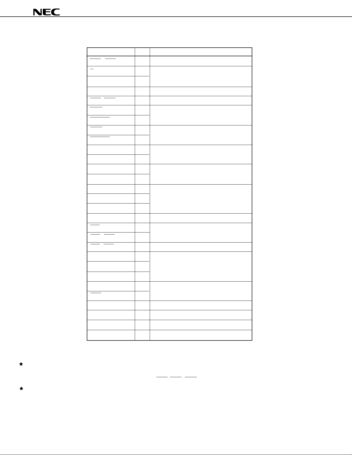
ORDERING INFORMATION
Part Number Package
µ
PD77016GM-KMD 160-pin plastic QFP (FINE PITCH) (24 × 24 mm)
Document No. U10891EJ5V0DS00 (5th edition)
Date Published April 1998 N CP(K)
Printed in Japan
The information in this document is subject to change without notice.
The mark shows major revised points.
©
1992, 1994, 1995
Page 2

2
X–Bus
BLOCK DIAGRAM
External
Memory
Serial
I/O #1
Serial
I/O #2
Ports
Host I/O
X Memory
Data
Pointers
Interrupt
Control
X Memory
2KW–RAM
Loop
Control
Stack
CPU Control
Main Bus
Y Memory
Data
Pointers
PC Stack
Y–Bus
Y Memory
2KW–RAM
Instruction
Memory
(1.5 KW–RAM)
MPY
16 × 16 + 40 → 40
R0–R7
ALU (40)
Wait
Controller
IE
I/O
INT1–INT4 RESET CLKOUT CLKIN
External Instruction MemoryWAIT
µ
PD77016
Page 3

FUNCTIONAL PIN GROUPS
SO1
SORQ1
SOEN1
SCK1
SI1
SIEN1
SIAK1
Serial
Interface #1
SO2
SORQ2
SOEN2
SCK2
SI2
SIEN2
SIAK2
Serial
Interface #2
HCS
HA0,HA1
HRD
HRE
HWR
HWE
HD0 - HD7
Host Interface
P0 - P3Ports
(2)
(4)
(8)
V
DD
+5 V
GND
RESET
INT1
INT2
INT3
INT4
IA0 - IA15
ID0 - ID31
HOLDRQ
BSTB
X/Y
DA0 - DA15
D0 - D15
WAIT
MRD
MWR
HOLDAK
External Instruction
Memory
Data Bus Control
Interrupts
(16)
(32)
(16)
External Data Memory
(16)
(2)
(3)
TDO,TICE
TCK,TDI,TMS
CLKIN
CLKOUT
PWR
Debugging
Interface
µ
PD77016
3
Page 4
4
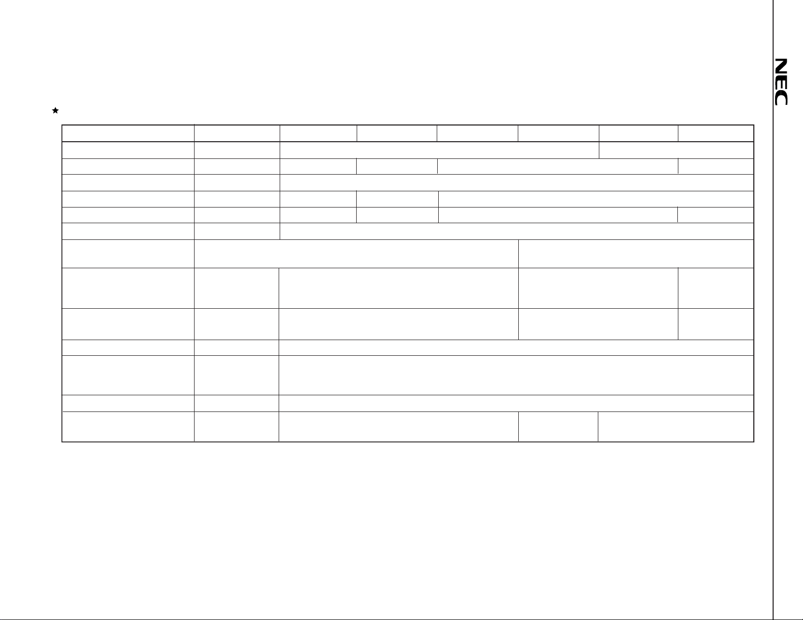
Functional Differences among the
Item
Internal instruction RAM 1.5K words 256 words 4K words
Internal instruction ROM None 4K words 12K words 24K words None
External instruction memory 48K words None
Data RAM (X/Y memory) 2K words each 1K words each 2K words each 3K words each
Data ROM (X/Y memory) None 2K words each 4K words each 12K words each None
External data memory 48K words each 16K words each
Instruction cycle
(Maximum operation speed)
External clock
(at maximum operation speed)
Crystal
(at maximum operation speed)
Instruction – STOP instruction is added.
Serial interface (2 Channels)
Power supply 5V 3 V
Package
µ
PD7701× Family
µ
PD77016
66 MHz
–
Channel 1 has the
same functions
as channel 2.
160-pin plastic QFP 100-pin plastic TQFP
µ
PD77015
30 ns (33 MHz)
Variable multiple rate (1, 2, 4, 8 ) by mask option.
Channel 1 has the same functions as that of the
Channel 2 has no SORQ2 or SIAK2 pin (Channel 2 is used for CODEC connection).
µ
PD77017
33/16.5/8.25/4.125 MHz
33 MHz
µ
PD77018
µ
PD77016.
µ
PD77018A
60/30/20/15/7.5 MHz
Variable multiple rate (1, 2, 3, 4, 8 ) by
mask option.
60 MHz
100-pin plastic TQFP
116-pin plastic BGA
µ
PD77019
16.6 ns (60 MHz)
100-pin plastic TQFP
µ
PD77019-013
15 MHz
Multiple rate is
fixed to 4.
–
Remark The
µ
PD77019-013 internal ROM area is masked already by the void code to use as RAM based DSP without mask code ordering process.
µ
PD77016
Page 5
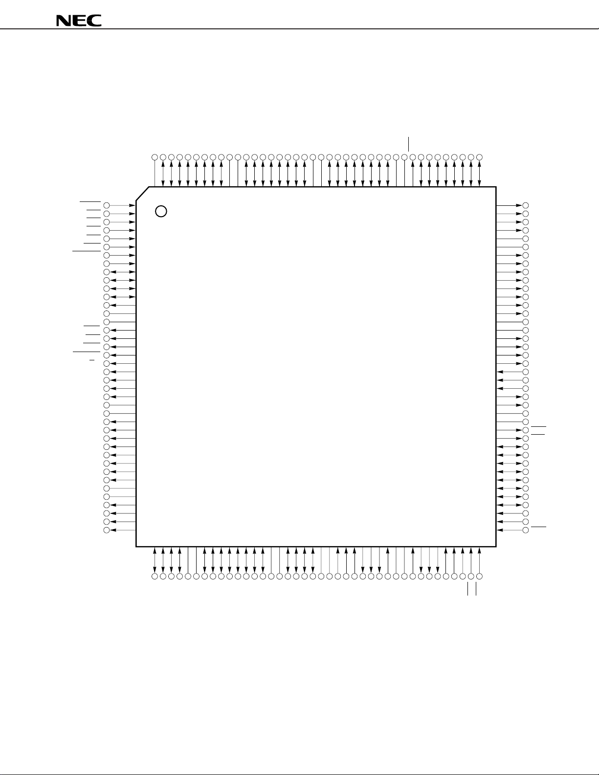
PIN CONFIGURATION
µ
PD77016GM-KMD
160-pin plastic QFP (FINE PITCH) (24 × 24 mm) (Top View)
µ
PD77016
RESET
INT4
INT3
INT2
INT1
WAIT
HOLDRQ
CLKIN
P3
P2
P1
P0
CLKOUT
GND
V
MWR
MRD
BSTB
HOLDAK
X/Y
DA15
DA14
DA13
DA12
GND
V
DA11
DA10
DA9
DA8
DA7
DA6
DA5
DA4
GND
V
DA3
DA2
DA1
DA0
NC
ID0
ID1
ID2
ID3
ID4
ID5
ID6
ID7
VDDGND
ID8
ID9
ID10
ID11
ID12
ID13
ID14
ID15
VDDGND
ID16
ID17
ID18
ID19
ID20
ID21
ID22
ID23
DD
PWR
ID24
GND
V
ID25
ID26
ID27
ID28
ID29
ID30
ID31
121122123124125126127128129130131132133134135136137138139140141142143144145146147148149150151152153154155156157158159160
1
2
3
4
5
6
7
8
9
10
11
12
13
14
DD
15
16
17
18
19
20
21
22
23
24
25
DD
26
27
28
29
30
31
32
33
34
35
DD
36
37
38
39
40
120
119
118
117
116
115
114
113
112
111
110
109
108
107
106
105
104
103
102
101
100
99
98
97
96
95
94
93
92
91
90
89
88
87
86
85
84
83
82
81
IA0
IA1
IA2
IA3
V
DD
GND
IA4
IA5
IA6
IA7
IA8
IA9
IA10
IA11
DD
V
GND
IA12
IA13
IA14
IA15
TMS
TDI
TCK
TIC
TDO
DD
V
GND
HWE
HRE
HD0
HD1
HD2
HD3
HD4
HD5
HD6
HD7
HA1
HA0
HWR
80797877767574737271706968676665646362616059585756555453525150494847464544434241
D15
D14
D13
D12
GND
DD
V
D11
D9D8D7D6D5
D10
D4
GND
DD
D3D2D1
V
D0
GND
DD
V
SI1
SCK1
SIEN1
SO1
SIAK1
GND
SOEN1
SORQ1
DD
V
SOEN2
SORQ2
SO2
SCK2
SIAK2
SI2
SIEN2
HCS
HRD
5
Page 6

PIN IDENTIFICATION
BSTB: Bus Strobe
CLKIN: Clock Input
CLKOUT: Clock Output
D0-D15: 16 Bits Data Bus
DA0-DA15: External Data Memory Address Bus
GND: Ground
HA0,HA1: Host Data Access
HCS: Host Chip Select
HD0-HD7: Host Data Bus
HOLDAK: Hold Acknowledge
HOLDRQ: Hold Request
HRD: Host Read
HRE: Host Read Enable
HWE: Host Write Enable
HWR: Host Write
IA0-IA15: Instruction Memory Address Output
ID0-ID31: Instruction Data Input
INT1-INT4: Interrupt
MRD: Memory Read Output
MWR: Memory Write Output
N.C: No Connection
P0-P3: Port
PWR: Program Memory Write Strobe
RESET: Reset
SCK1,SCK2: Serial Clock Input
SI1,SI2: Serial Data Input
SIAK1,SIAK2: Serial Input Acknowledge
SIEN1,SIEN2: Serial Input Enable
SO1,SO2: Serial Data Output
SOEN1,SOEN2: Serial Output Enable
SORQ1,SORQ2: Serial Output Request
TCK: Test Clock Input
TDI: Test Data Input
TDO: Test Data Output
TICE: Test In-Circuit Emulator
TMS: Test Mode Select
DD: Power Supply
V
WAIT: Wait Input
X/Y: X/Y Memory Select
µ
PD77016
6
Page 7
µ
PD77016
Pin No. Symbol
1 RESET
2 INT4
3 INT3
4 INT2
5 INT1
6 WAIT
7 HOLDRQ
8 CLKIN
9P3
10 P2
11 P1
12 P0
13 CLKOUT
14 GND
15 VDD
16 MWR
17 MRD
18 BSTB
19 HOLDAK
20 X/Y
21 DA15
22 DA14
23 DA13
24 DA12
25 GND
26 VDD
27 DA11
28 DA10
29 DA9
30 DA8
31 DA7
32 DA6
33 DA5
34 DA4
35 GND
36 VDD
37 DA3
38 DA2
39 DA1
40 DA0
Pin No. Symbol
41 D15
42 D14
43 D13
44 D12
45 GND
46 VDD
47 D11
48 D10
49 D9
50 D8
51 D7
52 D6
53 D5
54 D4
55 GND
56 VDD
57 D3
58 D2
59 D1
60 D0
61 GND
62 VDD
63 SI1
64 SIEN1
65 SCK1
66 SIAK1
67 SO1
68 SORQ1
69 SOEN1
70 GND
71 VDD
72 SOEN2
73 SORQ2
74 SO2
75 SIAK2
76 SCK2
77 SIEN2
78 SI2
79 HCS
80 HRD
Pin No. Symbol
81 HWR
82 HA0
83 HA1
84 HD7
85 HD6
86 HD5
87 HD4
88 HD3
89 HD2
90 HD1
91 HD0
92 HRE
93 HWE
94 GND
95 VDD
96 TDO
97 TICE
98 TCK
99 TDI
100 TMS
101 IA15
102 IA14
103 IA13
104 IA12
105 GND
106 VDD
107 IA11
108 IA10
109 IA9
110 IA8
111 IA7
112 IA6
113 IA5
114 IA4
115 GND
116 VDD
117 IA3
118 IA2
119 IA1
120 IA0
Pin No. Symbol
121 ID31
122 ID30
123 ID29
124 ID28
125 ID27
126 ID26
127 ID25
128 ID24
129 PWR
130 GND
131 VDD
132 ID23
133 ID22
134 ID21
135 ID20
136 ID19
137 ID18
138 ID17
139 ID16
140 GND
141 VDD
142 ID15
143 ID14
144 ID13
145 ID12
146 ID11
147 ID10
148 ID9
149 ID8
150 GND
151 VDD
152 ID7
153 ID6
154 ID5
155 ID4
156 ID3
157 ID2
158 ID1
159 ID0
160 NC
7
Page 8

µ
PD77016
CONTENTS
1. PIN FUNCTIONS............................................................................................................................... 9
1.1 Pin Functions........................................................................................................................................... 9
1.2 Recommended Connection for Unused Pins .......................................................................................14
2. FUNCTIONS...................................................................................................................................... 15
2.1 Pipeline Processing ................................................................................................................................ 15
2.1.1 Outline........................................................................................................................................... 15
2.1.2 Instructions with Delay .................................................................................................................. 15
2.2 Program Control Unit.............................................................................................................................. 16
2.3 Operation Unit ......................................................................................................................................... 16
2.3.1 General register (R0 to R7)........................................................................................................... 16
2.3.2 MAC: Multiply ACcumulator ......................................................................................................... 17
2.3.3 ALU: Arithmetic Logic Unit ........................................................................................................... 17
2.3.4 BSFT: Barrel ShiFTer................................................................................................................... 17
2.3.5 SAC: Shifter And Count Circuit .................................................................................................... 17
2.3.6 CJC: Condition Judge Circuit ....................................................................................................... 17
2.4 Memory..................................................................................................................................................... 18
2.4.1 Instruction RAM Outline ................................................................................................................ 19
2.4.2 Data Memory Outline .................................................................................................................... 19
2.4.3 Data Memory Addressing.............................................................................................................. 19
2.5 On-chip Peripheral Circuit...................................................................................................................... 20
2.5.1 Serial Interface Outline.................................................................................................................. 20
2.5.2 Host Interface Outline.................................................................................................................... 20
2.5.3 General Input/output Ports Outline................................................................................................ 20
2.5.4 Wait Cycle Register....................................................................................................................... 20
3. INSTRUCTIONS................................................................................................................................ 21
3.1 Outline...................................................................................................................................................... 21
3.2 Instruction Set and Operation................................................................................................................ 22
4. ELECTRICAL SPECIFICATIONS.....................................................................................................29
5. PACKAGE DRAWING ...................................................................................................................... 50
6. RECOMMENDED SOLDERING CONDITIONS................................................................................ 51
8
Page 9
1. PIN FUNCTIONS
1.1 Pin Functions
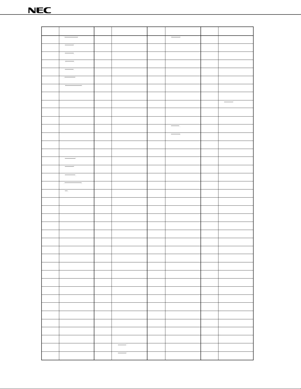
• Power supply
Symbol Pin No. I/O Function
µ
PD77016
VDD – +5V power supply
GND – Ground
15, 26, 36, 46, 56, 62, 71,
95, 106, 116, 131, 141, 151
14, 25, 35, 45, 55, 61, 70,
94, 105, 115, 130, 140, 150
• System control
Symbol Pin No. I/O Function
CLKIN 8 I External clock input
CLKOUT 13 O Internal system clock output
RESET 1 I Internal system reset signal input
• Interrupt
Symbol Pin No. I/O Function
INT4 - INT1 2, 3, 4, 5 I Maskable external interrupt input
• Falling edge detection
9
Page 10
• External data memory interface
Symbol Pin No. I/O Function
X/Y 20 O Memory select signal output
(3S) • 0: X memory is used.
• 1: Y memory is used.
DA15 - DA0 Note 1. O Address bus to external data memory
(3S) • External data memory is accessed.
• During the external memory is not accessed, these pins
keep the previous level.
These pins are set to low level; 0x0000, by reset.
They continue outputting low level until the first external
memory access.
D15 - D0 Note 2. I/O 16 bits data bus to external data memory
(3S) • External data memory is accessed.
MRD 17 O Read output
(3S) • Reads external memory
µ
PD77016
MWR 16 O Write output
(3S) • Writes external memory
WAIT 6 I Wait signal input
• Wait cycle is input when external memory is read.
1: No wait
0: Wait
HOLDRQ 7 I Hold request signal input
• Input low level when external data memory bus is
expected to use.
BSTB 18 O Bus strobe signal output
• Outputs low level while the µPD77016 is occupying
external memory bus.
HOLDAK 19 O Hold acknowledge signal output
• Outputs low level when the µPD77016 permits external
device to use external data memory bus.
Note 1. DA15 to DA0 pins are located on Pin No. 21 - 24, 27 - 34, 37 - 40.
2. D15 to D0 pins are located on Pin No. 41 - 44, 47 - 54, 57 - 60.
Remark The state of the pins added 3S becomes high impedance when the external memory is not accessed or bus release signal
(HOLDAK = 0) is output.
10
Page 11
• Serial interface
Symbol Pin No. I/O Function
SCK1 65 I Clock input for serial 1
SORQ1 68 O Serial output 1 request
SOEN1 69 I Serial output 1 enable
SO1 67 O (3S) Serial data output 1
SIEN1 64 I Serial input 1 enable
SI1 63 I Serial data input 1
SCK2 76 I Clock input for serial 2
SORQ2 73 O Serial output 2 request
SOEN2 72 I Serial output 2 enable
µ
PD77016
SO2 74 O (3S) Serial data output 2
SIEN2 77 I Serial input 2 enable
SI2 78 I Serial data input 2
SIAK1 66 O Serial input 1 acknowledge
SIAK2 75 O Serial input 2 acknowledge
Remark The state of the pins added 3S becomes high impedance, when data output have been finished or RESET is input.
11
Page 12
• Host interface
Symbol Pin No. I/O Function
HA1 83 I Specifies register which HD7 to HD0 access
1: Accesses HST: Host interface status register
when HA1 = 0
0: Accesses HDT(out): Host transmit data register when
HRD = 0
0: Accesses HDT(in): Host receive data register when
HWR = 0
HA0 82 I Specifies bits of registers which HD7 to HD0 access
• 1: Accesses bits 15-8 of HST, HDT (out), HDT (in)
• 0: Accesses bits 7-0 of HST, HDT (out), HDT (in)
HCS 79 I Chip select input
HRD 80 I Host read input
HWR 81 I Host write input
µ
PD77016
HRE 92 O Host read enable output
HWE 93 O Host write enable output
HD7 - HD0 84 - 91 I/O (3S) 8 bits host data bus
Remark The state of the pins added 3S becomes high impedance when the host does not access host interface.
• I/O port
Symbol Pin No. I/O Function
P3 - P0 9 - 12 I/O I/O port
12
Page 13
• External instructions memory interface
Symbol Pin No. I/O Function
IA15 - IA0 Note 1. O (3S) Address bus to external instruction memory
• Even the internal instruction memory is accessed, the
address is output to the external instruction memory.
In this case, the µPD77016 ignores data of external
instruction memory output.
ID31 - ID0 Note 2. I/O (3S) 32 bits instruction input
PWR 129 O (3S) Program memory write strobe
• Write strobe for external instruction memory. This pin
loads program to external instruction memory (not
internal memory) while µPD77016 is in boot operation.
Note 1. IA15 to IA0 pins are located on these pins: 101 to 104, 107 to 114, 117 to 120
2. ID31 to ID0 pins are located on these pins: 121 to 128, 132 to 139, 142 to 149, 152 to 159
Remark The state of the pins added 3S becomes high impedance when RESET is input.
µ
PD77016
• Debugging interface
Symbol Pin No. I/O Function
TDO 96 O For debugging
TICE 97 O For debugging
TCK 98 I For debugging
TDI 99 I For debugging
TMS 100 I For debugging
13
Page 14
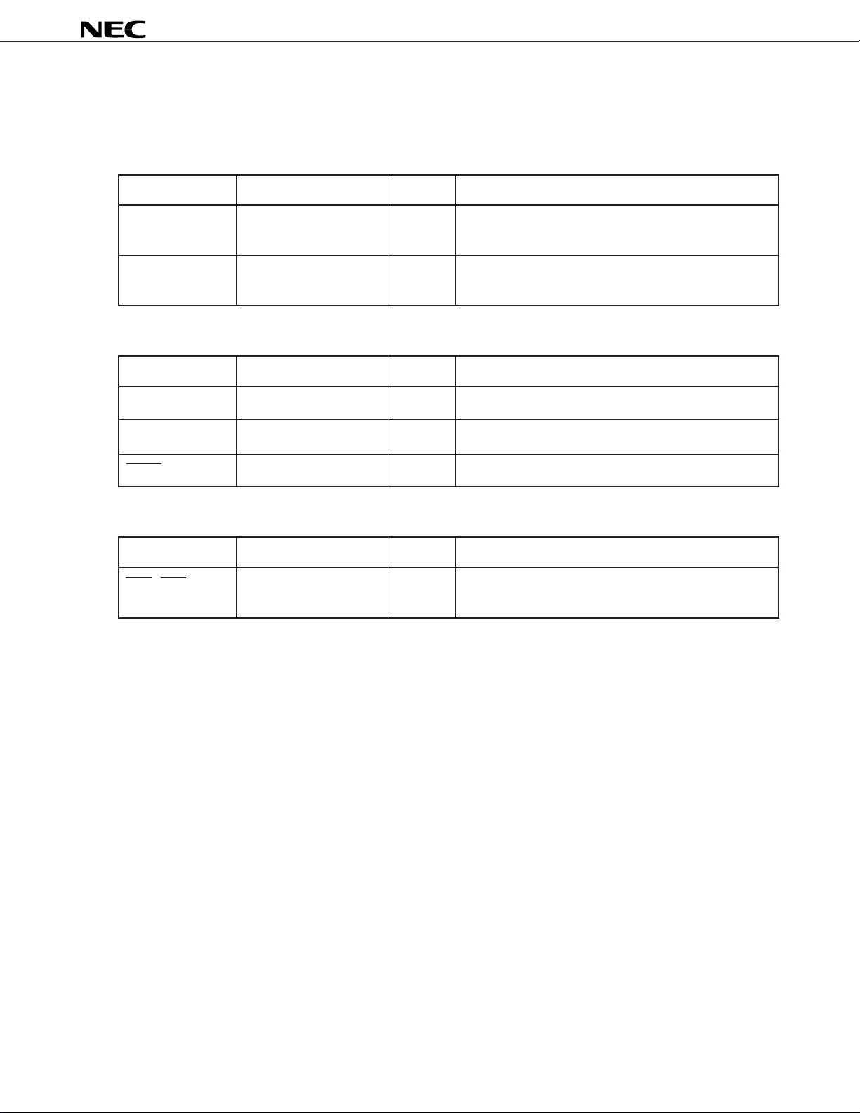
1.2 Recommended Connection for Unused Pins
µ
PD77016
Pin I/O
INT1 - INT4 I
X/Y O
DA0 - DA15 O
D0 - D15
MRD, MWR O
WAIT I
HOLDRQ I
BSTB O
HOLDAK O
SCK1, SCK2 I
SI1, SI2 I
SOEN1, SOEN2 I
SIEN1, SIEN2 I
SORQ1, SORQ2 O
SO1, SO2 O
SIAK1, SIAK2 O
HA0, HA1 I
HCS I
HRD, HWR I
Note 1
I/O
Recommended connection
connect to VDD
open
connect to VDD or GND, via a resistor
open
connect to VDD
open
connect to VDD or GND
connect to GND
open
connect to VDD or GND
connect to VDD
HRE, HWE O
HD0 - HD7
P0 - P3 I/O
ID0 - ID31 I/O
IA0 - IA15 O
PWR O
TCK I
TDO, TICE O
TMS, TDI I
CLKOUT O
Note 2
open
I/O
connect to VDD or GND, via a resistor
open
connect to GND, via a resistor
open
open(pull-up internally)
open
Notes 1. Can leave open, if no access to external data memory is
executed in the whole of program.
But in the HALT mode when the current consumption is
reduced, connect a pin as recommended connection.
2. Can leave open, if HCS, HRD, HWR are fixed to high level.
But in the HALT mode when the current consumption is
reduced, connect a pin as recommended connection.
Remark I: Input pin, O: Output pin, I/O: Input/Output pin
14
Page 15

µ
PD77016
2. FUNCTIONS
2.1 Pipeline Processing
This section describes the µPD77016 pipeline processing.
2.1.1 Outline
µ
PD77016 basic operations are executed in following 3-stage pipeline.
The
(1) instruction fetch; if
(2) Instruction decoding; id
(3) execution; ex
µ
When the
with written back to general registers. Pipeline processing actualizes programming without delay time to execute
instructions and write back data. Three successive instructions and their processing timing are shown below.
PD77016 operates a result of a instruction just executed before, the data is input to ALU in parallel
Pipeline Processing Timing
if1 id1 ex1
if2 id2 ex2
if3 id3 ex3
1 instruction cycle
2.1.2 Instructions with Delay
The following instructions have delay time in execution.
(1) Instructions to control interrupt
2 instruction cycles have been taken between instruction fetch and execution.
(2) Inter-register transfer instructions and immediate data set instructions
When data is set in data pointer, it needs 2 instruction cycles before the data is valid.
15
Page 16
µ
PD77016
2.2 Program Control Unit
Program control unit controls not only count up of program counter in normal operation, but loop, repeat,
branch, halt and interrupt.
In addition to loop stack of loop 4 level and program stack of 15 level, software stack can be used for multi-
loop and multi-interrupt/subroutine call.
µ
PD77016 has external 4 interruptions and internal 6 interruptions from peripheral, and specifies interrupt
The
enable or disable independently.
The HALT instruction causes the µPD77016 to place in low power standby mode.
When the HALT instruction is executed, power consumption decreases. HALT mode is released by interrupt
input or hardware reset input. It takes several system clock to recover.
2.3 Operation Unit
Operation unit consists of the following five parts.
– 40 bits general register × 8 for data load/store and input/output of operation data
– 16 bits × 16 bits + 40 bits → 40 bits multiply accumulator
– 40 bits Data ALU
– 40 bits barrel shifter
– SAC: shifter and count circuit.
Standard word length is 40 bits to make overflow check and adjustment easy, and to accumulate the result
of 16 bits × 16 bits multiplication correctly.
SSSSSSSS
Head room
2.3.1 General register (R0 to R7)
µ
PD77016 has eight 40 bits registers for operation input/output and load/store with memory. General
The
register consists of the following three parts.
– R0L to R7L (bit 15 to bit 0)
– R0H to R7H (bit 31 to bit 16)
– R0E to R7E (bit 39 to bit 32)
But each of RnL, RnH and RnE are treated as a register in the following conditions.
(1) General register used as 40 bits register
General registers are treated as 40 bits register, when they are used for the following aims.
(a) Operand for triminal operation (except for multiplier input)
(b) Operand for dyadic operation (except for multiplier and shift value)
(c) Operand for monadic operation (except for exponent instructions)
(d) Operand for operation
(e) Operand for conditional judge
(f) Destination for load instruction (with sign extension and 0 clear)
Result of multiplication among two's complement data
0
1313239
0
(2) General register used as 32 bits register
Bit 31 to bit 0 of general register are treated as 32 bits register, when it is used for a operand of exponent
instruction.
16
Page 17

µ
PD77016
(3) General register used as 24 bits register
Bit 39 to bit 16 of general register are treated as 24 bits register, when it is used for destination with extended
sign for a load/store instruction.
(4) General register used as 16 bits register
Bit 31 to bit 16 of general register are treated as 16 bits register, when it is used for the following aims.
(a) Signed operand for multiplier
(b) Source/destination for load/store instruction
Bit 15 to bit 0 of general register are treated as 16 bits register, when it is used for the following aims.
(c) Unsigned operand for multiplier
(d) Shift value for shift instruction
(e) Source/destination for load/store instruction
(f) Source/destination for inter-register transfer instruction
(g) Destination for immediate data set instruction
(f) Hardware loop times
(5) General register used as 8 bits register
Bit 39 to bit 32 of general register are treated as 8 bits register, when it is used for source/destination of load/
store instruction.
2.3.2 MAC: Multiply ACcumulator
MAC multiplies a pair of 16 bits data, and adds or subtract the result and 40 bits data. MAC outputs 40 bits
data.
MAC operates three types of multiplication: signed data × signed data, signed data × unsigned data and
unsigned data × unsigned data.
Result of multiplication and 40 bits data for addition can be added after 1 or 16 bits arithmetic shift right.
2.3.3 ALU: Arithmetic Logic Unit
ALU performs arithmetic operation and logic operation. Both input/output data are 40 bits.
2.3.4 BSFT: Barrel ShiFTer
BSFT performs shift right/left operation. Both input/output data are 40 bits. There are two types of shift right
operations; arithmetic shift right which sign is extended, and logic shift right which is input 0 in MSB first.
2.3.5 SAC: Shifter And Count Circuit
SAC calculates and outputs shift value for normalization. SAC is input 32 bits data and outputs the 40 bits
data. Then, bit 39 to bit 5 of output data is always 0.
2.3.6 CJC: Condition Judge Circuit
CJC judges whether condition is true or false with 40 bits input data. A conditional instruction is executed
when the result is true, and not executed when the result is false.
17
Page 18

µ
PD77016
2.4 Memory
µ
PD77016 has one instruction memory area (64K words × 32 bits) and two data memory areas (64K words
The
× 16 bits each). It adopts Harvard-type architecture, with instruction memory area and data memory areas
separated.
µ
PD77016 has 2 sets of data addressing units, which are dedicated for addressing data memory area.
The
Each addressing unit consists of four data pointers, four index registers, a modulo register and addressing ALU.
Memory areas are shown below.
X memory area addresses are specified by DP0 to DP3, and Y memory area addresses are specified by DP4
to DP7. After memory access, DPn (with the same subscript), can be modified by DNn value. Modulo operation
is performed with DMX for DP0 to DP3, with DMY for DP4 to DP7.
Data Memory Area (X/Y Memory) Instruction Memory Area
0xFFFF
0x4000
0x3FFF
0x3840
0x383F
0x3800
0x37FF
0x0800
0x07FF
0x0000
External Data Memory
(48 K words)
System
Peripheral (64 words)
System
Data RAM (2 K words)
0xFFFF
0x4000
0x3FFF
0x0800
0x07FF
0x0240
0x023F
0x0200
0x01FF
0x0100
0x00FF
0x0000
External Instruction Memory
(48 K words)
System
Internal Instruction RAM (1.5 K words)
Vector (64 words)
System
Bootup ROM (256 words)
Caution When any data is accessed or stored to system address, normal operation of the
not assured.
18
µ
PD77016 is
Page 19

µ
PD77016
2.4.1 Instruction RAM Outline
The µPD77016 has an instruction RAM (1.5 words × 32 bits). A system vector area is assigned to 64 words
of the instruction RAM. Internal RAM is initialized and rewritten by boot program.
µ
Additionally external memory expansion is available as the
instruction memory. When RAM is used as the external memory, it can be initialized and rewritten by boot
program.
Boot up ROM contains the program loading instruction code to internal and external instruction RAM.
When the external instruction memory area is accessed, instruction cycle can be 2 or more by wait function.
2.4.2 Data Memory Outline
µ
PD77016 has two data memory areas (64 words × 16 bits each) in X and Y memory areas.
The
Each memory areas consists of 2K words × 16 bits data RAM. Additionally, data memory expansion is
µ
available as the
Each data memory area includes on-chip peripheral area which consists of 64 words.
When the external data memory area is accessed, instruction cycle can be 2 or more by wait function.
2.4.3 Data Memory Addressing
There are following two types of data memory addressing.
• Direct addressing
The address is specified in the instruction field.
• Indirect addressing
The address is specified by the data pointer (DP). DP can get a bit reverse before addressing. It can update
the DP value after accessing data memory.
PD77016 has interface with the external data memory.
PD77016 has interface with the external
19
Page 20

µ
PD77016
2.5 On-chip Peripheral Circuit
µ
PD77016 includes serial interface, host interface, general input/output ports and wait cycle registers.
The
They are mapped in both X and Y memory areas, and are accessed as memory mapped I/O by the µPD77016
CPU.
2.5.1 Serial Interface Outline
µ
PD77016 has 2 channel serial interfaces. Serial I/O clock must be provided from external. Frame length
The
can be programmed independently to be 8 bits or 16 bits. MSB first or LSB first can also be selected. Data is
input/output by hand shaking for an external device, and by interrupts, polling or wait function in internal.
2.5.2 Host Interface Outline
µ
PD77016 has 8 bits parallel ports as host interface to input/output data to and from host CPU and DMA
The
controller. When an external device accesses host interface, HA0 and HA1 pins; which are host address input
µ
pins; specifies bit 15 to bit 8 and bit 7 to bit 0. The
are dedicated for input data, output data and status. The µPD77016 has three types of interface method for
internal and external data; interrupts, polling and wait function.
2.5.3 General Input/output Ports Outline
General input/output ports consist of 4 bits. User can set each port as input or output. The
two registers. One is 4 bits register for input/output data, and the other is 16 bits for control.
PD77016 includes 3 registers consisting of 16 bits, which
µ
PD77016 includes
2.5.4 Wait Cycle Register
The wait cycle registers consist of 16 bits. It is used to set wait cycle number when external memory is
accessed. 0, 1, 3, or 7 wait cycle can be set in every data area which is divided into 8, and in every X and Y
memory area which is divided into 4.
When data area is accessed, wait cycle can be also set by WAIT pin.
20
Page 21

µ
PD77016
3. INSTRUCTIONS
3.1 Outline
All µPD77016 instructions are one-word instructions, consisting of 32 bits. And they are executed in 30 ns
(min.) per instruction. There are following 9 instruction types.
(1) Trinomial instructions
: specify the Acc operation. 3 of general registers are specified optionally as the operation object.
(2) Dyadic operation instructions
: specify the Acc, ALU or shifter operation. 2 of general registers are specified optionally as the operation
object. Some instructions can specify a general register and immediate data.
(3) Monadic operation instructions
: specify operations by ALU. 1 general register is specified optionally as the operation object.
(4) Load/store instructions
: transfer 16 bits data from memory to general registers, from general registers to memory and between general
registers.
(5) Inter-register transfer instructions
: transfer data between general register and other registers.
(6) Immediate data set instructions
: set immediate data at general registers or each registers of address operation unit.
(7) Branch instructions
: specify the direction of the program flow.
(8) Hardware loop instructions
: specify times of instruction repeating.
(9) Control Instructions
: specify the control program.
21
Page 22

µ
PD77016
3.2 Instruction Set and Operation
An operation is written according to the rules for expressing. An expression of instructions having two or more
descriptions can have only one selected.
(a) Expressions and selectable registers
Expression and selectable registers are shown as follows.
Expression Selectable registers
ro, ro', ro" R0 - R7
rl, rl' R0L - R7L
rh, rh' R0H - R7H
re R0E - R7E
reh R0EH - R7EH
dp DP0 - DP7
dn DN0 - DN7
dm DMX, DMY
dpx DP0 - DP3
dpy DP4 - DP7
dpx_mod DPn, DPn++, DPn– –, DPn##, DPn%%, !DPn## (n = 0 - 3)
dpy_mod DPn, DPn++, DPn– –, DPn##, DPn%%, !DPn## (n = 4 - 7)
dp_imm DPn##imm (n = 0 - 7)
∗××× content of memory address ×××
Example When the content of DP0 register is 1000, ∗DP0 shows the content of memory
address 1000.
22
Page 23

µ
PD77016
(b) Modifying data pointers
Data pointers are modified after memory access. The results are valid immediately after instruction execution.
It is impossible to modify without memory access.
Description Operation
DPn No operation: DPn value does not change.
DPn++ DPn ← DPn+1
DPn–
– DPn ← DPn–1
DPn## DPn ← DPn + DNn: Adds DN0-DN7 corresponding to DP0-DP7
Example DP0 ← DP0 + DN0
DPn%% (n = 0 - 3) DP
(n = 4 - 7) DPn = ((DPL + DNn ) mod (DMY + 1)) + DPH
!DPn## Access memory after DPn value is bit-reversed
After memory access, DPn ← DPn + DNn
DPn##imm DPn ← DPn + imm
(c) Concurrent processing instructions
●● shows concurrent processing instruction.
Instruction names are shown in abbreviation.
TRI : Trinomial
DYAD : Dyadic
MONAD : Monadic
TRANS : Inter-register transfer
IMM : Immediate data set
BR : Branch
LOOP : Hardware loop
CTR : Control
(d) State of Overflow flag (OV)
The following marks show the
: Not affected
: 1 is set when the result of operation is overflow.
↔
n = ((DPL + DNn ) mod (DMX + 1)) + DPH
µ
PD77016 overflow flag state.
Caution If overflow does not occur after operation, OV is not reset, and keeps the state before operation.
23
Page 24

24
µ
PD77016 INSTRUCTION SET
Name Mnemonic Operation
Multiply add ro = ro + rh∗rh' ro ← ro+rh∗rh'
Multiply sub ro = ro–rh∗rh' ro ← ro–rh∗rh'
Sign unsign ro = ro + rh∗rl ro ← ro+rh∗rl
Multiply add (rl should be a plus
Trinomial
Unsign unsign ro=ro+rl∗rl' ro ← ro+rl∗rl'
Multiply add (rl and rl' should be a plus
1 bit shift Multiply add ro=(ro>>1)+rh∗rh' ro ← +rh∗rh'
16 bits shift Multiply add ro = (ro>>16)+rh∗rh' ro ← +rh∗rh'
Multiply ro=rh∗rh' ro ← rh∗rh'
Add ro"=ro+ro' ro" ← ro+ro'
Immediate add ro'=ro+imm ro' ← ro+imm (imm 1)
Sub ro"=ro–ro' ro" ← ro–ro'
integral number.)
integral number.)
Concurrent Writing Processing Flag
TRI. DYAD. MONAD. Load/ TRANS. IMM. BR. LOOP. CTL. OV
store
↔↔ ↔ ↔ ↔ ↔↔↔↔
ro
2
ro
16
2
Dyadic
Immediate sub ro'=ro–imm ro' ← ro–imm (imm 1)
Arithmetic right shift ro'=ro SRA rl ro' ← ro >> rl
Immediate arithmetic ro'=ro SRA imm ro' ← ro >> imm
right shift
Logic right shift ro'=ro SRL rl ro' ← ro >> rl
Immediate Logic right shift ro'=ro SRL imm ro' ← ro >> imm
Logic left shift ro'=ro SLL rl ro' ← ro << rl
Immediate logic left shift ro'=ro SLL imm ro' ← ro << imm
µ
PD77016
Page 25

Name Mnemonic Operation
And ro" = ro & ro' ro" ← ro & ro'
Immediate and ro' = ro & imm ro' ← ro & imm
Or ro" = ro | ro' ro" ← ro | ro'
Concurrent Writing Processing Flag
TRI. DYAD. MONAD. Load/ TRANS. IMM. BR. LOOP. CTL. OV
store
25
Dyadic
Monadic
Immediate or ro' = ro | imm ro' ← ro | imm
Exclusive or ro" = ro ^ ro' ro" ← ro ^ ro'
Immediate exclusive or ro = ro ^ imm ro ← ro ^ imm
Less than ro" = LT(ro, ro') if(ro<ro')
Clear CLR(ro) ro ← 0x0000000000
Increment ro' = ro + 1 ro' ← ro + 1
Decrement ro' = ro – 1 ro' ← ro – 1
Absolute ro' = ABS (ro) if (ro<0)
One's complement ro' =
Two's complement ro' = –ro ro' ← –ro
Clip ro' = CLIP (ro) if (ro>0x007FFFFFFF)
Round ro' = ROUND (ro) if (ro>0x007FFF0000)
Exponent ro' = EXP (ro) ro' ← log
Substitution ro' = ro ro' ← ro
~
ro ro' ←
{ro" ← 0x0000000001}
else {ro" ← 0x0000000000}
{ro' ← –ro}
else {ro' ← ro}
~
ro
{ro' ← 0x007FFFFFFF]
else if, (ro<0xFF80000000)
{ro' ← 0xFF80000000}
else {ro' ← ro}
{ro' ← 0x007FFF0000}
else if, (ro>0xFF80000000)
{ro' ← 0xFF80000000}
else {ro' ←
(ro + 0x8000) & 0xFFFFFF0000}
1
2
( )
ro
↔↔ ↔ ↔↔ ↔
µ
PD77016
Page 26

26
Name Mnemonic Operation
Cumulation ro'+ = ro ro' ← ro'+ro
Degression ro'– = ro ro' ← ro'–ro
Concurrent Writing Processing Flag
TRI. DYAD. MONAD. Load/ TRANS. IMM. BR. LOOP. CTL. OV
store
↔↔ ↔
Monadic
Load/store
Division ro'/ = ro if (sign(ro')==sign(ro))
{ro' ← (ro'–ro)<<1}
else
{ro' ← (ro'+ro)<<1}
if (sign(ro')==0
{ro' ← ro'+1}
Parallel load/store ro=∗dpx_mod ro'=∗dpy_mod ro ← ∗dpx, ro' ← ∗dpy
Note1, Note2.
ro=∗dpx_mod ∗dpy_mod=rh ro ← ∗dpx, ∗dpy ← rh
∗dpx_mod=rh ro=∗dpy_mod ∗dpx ← rh, ro ← ∗dpy
∗dpx_mod=rh ∗dpy_mod=rh' ∗dpx ← rh, ∗dpy ← rh'
Section load/store dest=∗dpx_mod dest'=∗dpy_mod dest ← ∗dpx, dest' ← ∗dpy
Note1, Note2, Note 3.
dest=∗dpx_mod ∗dpy_mod=source dest ← ∗dpx, ∗dpy ← source
∗dpx_mod=source dest=∗dpy_mod ∗dpx ← source, dest ← ∗dpy
∗dpx_mod=source ∗dpy_mod=source' ∗dpx ← source, ∗dpy ← source'
Note 1. One or both of a mnemonic pair can be written.
2. After execution of load/store, data is modified by mod.
3. One of following mnemonic should be selected: dest, dest' = {ro, reh, re, rh, rl}, source, source' = {re, rh, rl}.
µ
PD77016
Page 27

Load/store
Name Mnemonic Operation
Direct addressing dest = ∗addr dest ← ∗addr
load/store Note 1.
∗addr = source ∗addr ← source
Immediate index dest = ∗dp_imm dest ← ∗dp
load/store Note 2.
∗dp_imm = source ∗dp ← source
Concurrent Writing Processing Flag
TRI. DYAD. MONAD. Load/ TRANS. IMM. BR. LOOP. CTL. OV
store
Inter-register
transfer
Immediate
data set
Note 1. One of following mnemonic should be selected: dest = {ro, reh, re, rh, rl}, source = {re, rh, rl}, add = .
Inter-register transfer dest = rl dest ← rl
Note 3.
rl = source rl ← source
Immediate data set rl = imm rl ← imm
(provided imm = 0-0xFFFF)
dp = imm dp ← imm
(provided imm = 0-0xFFFF)
dn = imm dn ← imm
(provided imm = 0-0xFFFF)
dm = imm dm ← imm
(provided imm = 1-0xFFFF)
2. One of following mnemonic should be selected: dest = {ro, reh, re, rh, rl}, source = {re, rh, rl}.
0: X-0xFFFF:X memory
0: Y-0xFFFF:Y memory
3. Any register except general registers should be selected as dest or source.
µ
PD77016
27
Page 28

28
Branch
Hardware
loop
Control
Name Mnemonic Operation
Jump JMP imm PC ← imm
Inter-register indirect jump JMP dp PC ← dp
Subroutine call CALL imm SP ← SP + 1
STK ← PC +
PC ← imm
Inter-register indirect CALL dp SP ← SP + 1
subroutine call STK ← PC + 1
PC ← dp
Return RET PC ← STK
SP ← SP – 1
Return from interrupt RETI PC ← STK
STK ← SP – 1 Restore the
interrupt enable flag
Repeat REP count start RC ← count
RF ← 0
repeat PC ← PC
RC ← RC – 1
end PC ← PC + 1
RF ← 1
Loop LOOP count start RC ← count
(Mnemonics more than two lines) RF ← 0
repeat PC ← PC
RC ← RC – 1
end PC ← PC + 1
RF ← 1
Loop pop LPOP LC ← LSR3
LE ← LSR2
LS ← LSR1
LSP ← LSP–1
No operation NOP PC ← PC + 1
Halt HALT CPU stop
If IF (ro cond) Conditional judge
Forget interrupt FINT Forget interrupt request
Concurrent Writing Processing Flag
TRI. DYAD. MONAD. Load/ TRANS. IMM. BR. LOOP. CTL. OV
store
µ
PD77016
Page 29

µ
PD77016
4. ELECTRICAL SPECIFICATIONS
Absolute maximum ratings (TA = +25 ˚C)
Parameters Symbol Conditions Ratings Unit
Power supply voltage VDD –0.5 to +7.0 V
Input voltage VI –0.5 to VDD + 0.5 V
Output voltage VO –0.5 to VDD + 0.5 V
Storage temperature Tstg –65 to +150 ˚C
Operating ambient temperature TA –40 to +85 ˚C
Caution Exposure to Absolute Maximum Ratings for extended periods may affect device reliability;
exceeding the ratings could cause permanent damage. The parameters apply independently.
The device should be operated within the limits specified under DC and AC Characteristics.
Capacitance (T
Input capacitance CI 15 pF
Output capacitance CO 15 pF
A = +25 ˚C, VDD = 0 V)
Parameters Symbol Conditions MIN. TYP. MAX. Unit
fc = 1 MHz
Unmeasured pins returned to 0
V.
DC characteristics (TA=–40 to +85 ˚C, VDD = 5 V ±10 %)
Parameters Symbol Conditions MIN. TYP. MAX. Unit
High level input voltage
Low level input voltage
High level CLKIN voltage
Low level CLKIN voltage
High level output voltage
Low level output voltage
Low level input current
High level input leak current
Low level input leak current
Power supply current
VIH
VIHC
VIL
VILC
VIHX
VILX
VOH
VOL
IIL
ILIH
ILIL
IDD
IDDH
IDDS
except for RESET, CLKIN,
INT1 - INT4, WAIT, HCS,
HRD, HWR, TCK, TDI, TMS
RESET, INT1 - INT4, WAIT, HCS,
HRD, HWR, TCK, TDI, TMS
except for RESET, CLKIN,
INT1 - INT4, WAIT, HCS,
HRD, HWR, TCK, TDI, TMS
RESET, INT1 - INT4, WAIT, HCS,
HRD, HWR, TCK, TDI, TMS
IOH = –2.5 mA
IOL = 2.5 mA
TDI, TMS, VI = 0 V
VI = VDD
except for TDI, TMS, VI = 0 V
Note
Active mode, tcCI = 15 ns
VIH = VDD, VIL = 0 V, no load
HALT mode, tcCI = 15 ns,
VIH = VDD, VIL = 0 V, no load
CLKIN = 0 V
VIH = VDD, VIL = 0 V, no load
2.2
0.7VDD
–0.5
–0.5
0.8VDD
–0.5
0.8VDD
140
80
10
VDD + 0.5
VDD + 0.5
+0.8
0.2VDD
VDD + 0.5
0.2VDD
0.4
–400
10
–10
300
V
V
V
V
V
V
V
V
µ
µ
µ
mA
mA
µ
A
A
A
A
Note The TYP. value is measured when a general program is executed, and VDD = 5 V conditon. The MAX.
value is measured when a special program that max. switching required is executed, and VDD = 5.5 V
condition
.
29
Page 30

Measurement Standards Common to Switching Characteristics
0.8 V
0.5 V
0.2 V
DD
DD
DD
Test pointsCLKIN
0.8 V
0.5 V
0.2 V
µ
PD77016
DD
DD
DD
(except for CLKIN)
Input
2.2 V
1.5 V
0.8 V
2.2 V
1.5 V
0.8 V
Test points
Test pointsOutput
2.2 V
1.5 V
0.8 V
2.2 V
1.5 V
0.8 V
AC Characteristics (TA = –40 to +85 ˚C, VDD = 5 V ±10%, CL = 30 pF)
Clock
Required Timing Condition
Parameters Symbol Conditions MIN. TYP. MAX. Unit
CLKIN cycle time tcCI 15 500 ns
CLKIN high level width t wCIH 6.75 0.55 tcCI ns
CLKIN low level width twCIL 6.75 0.55 tcCI ns
CLKIN rise/fall time trfCI 6ns
Switching Characteristics
Parameters Symbol Conditions MIN. TYP. MAX. Unit
CLKOUT cycle time tcCO 2tcCI ns
CLKOUT level width twCO tcCI – 3 ns
CLKOUT rise/fall time trfCO 3ns
30
Page 31

µ
PD77016
Reset, Interrupt
Required Timing Condition
Parameters Symbol Conditions MIN. TYP. MAX. Unit
RESET low level width tw(RL) 4tcCO ns
RESET recovery time trec(R) 4tcCO ns
INT1-INT4 low level width tw(INTL) 3tcCO ns
INT1-INT4 recovery time trec(INT) 3tcCO ns
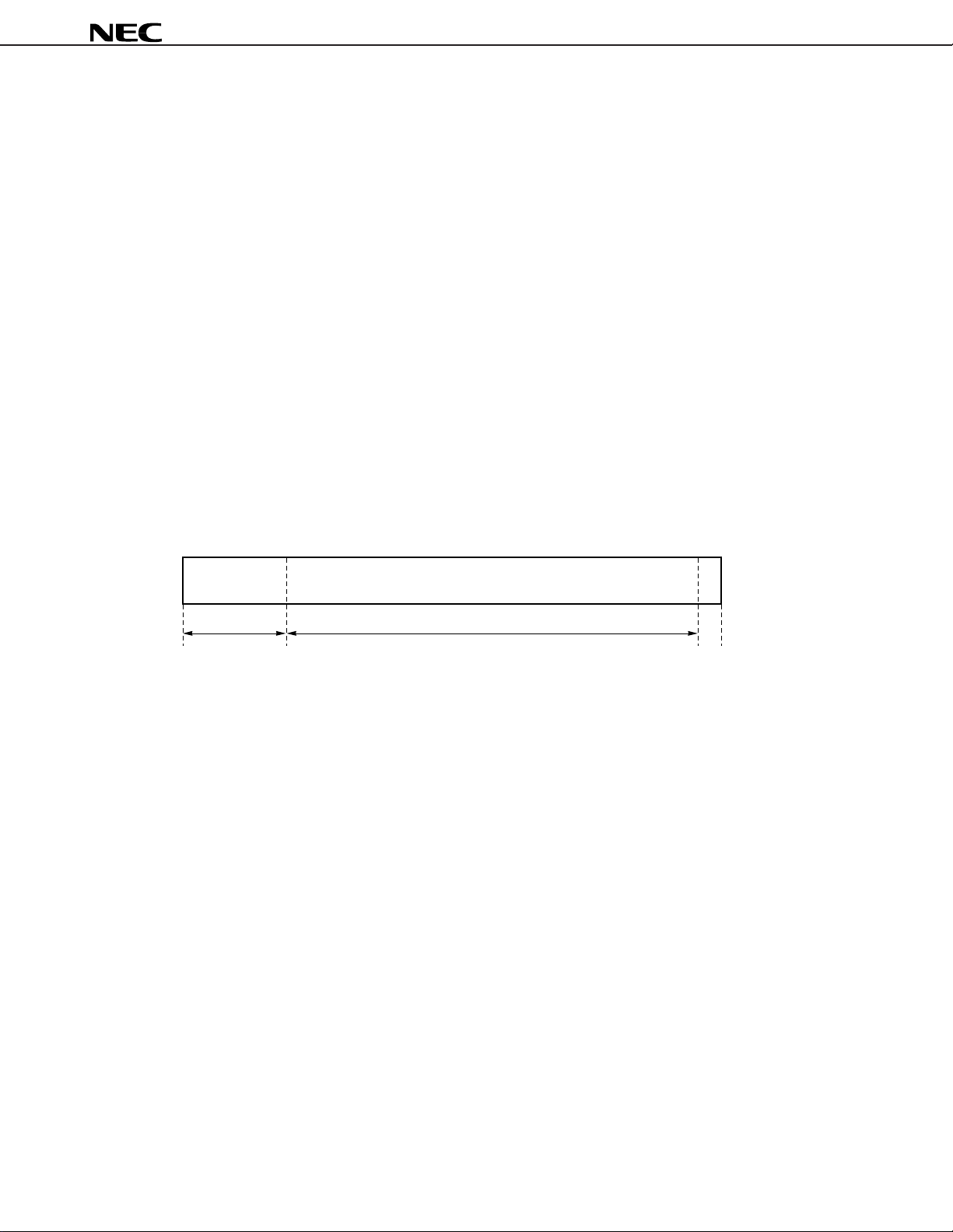
Clock Input/Output Timing
t
CLKIN
t
wCIH
cCI
t
wCIL
t
cCO
t
wCO
t
rfCI
t
wCO
t
rfCI
t
rfCO
t
rfCO
CLKOUT
Reset, Interrupt Timing
RESET
Interrupt Timing
INT1 - INT4
t
w(RL)
t
w(INTL)
t
rec(R)
t
rec(INT)
31
Page 32

µ
PD77016
External Data Memory Access
Required Timing Condition
Parameters Symbol Conditions MIN. TYP. MAX. Unit
Read data setup time tsuDDRD 14 ns
Read data hold time thDDRD 0ns
WAIT setup time tsuWA 8ns
WAIT hold time thWA 0ns
Switching Characteristics
Parameters Symbol Conditions MIN. TYP. MAX. Unit
Address output delay time tdDA 06ns
MRD output delay time tdDR 08ns
MRD hold time thDR 08ns
Write data setup time tsDDWD
Write data output hold time thDDWD 015ns
MWR output delay time tdDW twCIH – 4 ns
MWR setup time tsuDW twCIL – 4 ns
MWR low level width twDWL tcCI – 4 ns
MWR high level width twDWH tcCI – 4 ns
tcCI + twCIH –
+ tcDW
Note
Note
15 + tcDW
ns
Note tcDW: Data wait cycle
32
Page 33

External Data Memory Read Operation
CLKOUT
tdDA
DA0 DA15,
X/Y
µ
PD77016
D0 - D15
tdDR
MRD
tsuWA
WAIT
External Data Memory Write Operation
CLKOUT
thWA
tsuWA thWA
tsuDDRD
thDDRD
thDR
DA0 - DA15,
X/Y
D0 - D15
MWR
WAIT
t
dDA
t
sDDWD
Hi-Z Hi-Z
t
t
suWA
dDW
t
wDWL
t
hWA
t
suWA
t
hWA
t
wDWH
t
suDW
t
hDDWD
33
Page 34

µ
PD77016
External Instruction Memory Access
Required Timing Condition
Parameters Symbol Conditions MIN. TYP. MAX. Unit
ID setup time (to CLKOUT ↑)tsuID 14 ns
ID hold time (to CLKOUT ↑)thID 0ns
Switching Characteristics
Parameters Symbol Conditions MIN. TYP. MAX. Unit
IA output delay time tdIA 10 ns
IA hold time thIA 06ns
ID write setup time tsIDW
ID write hold time thIDW 0ns
PWR output delay time tdIW 10 ns
Address → PWR setup time td(IAV-IWV) tcCI + twCIH ns
PWR setup time tsuIW twCIL – 4 ns
PWR width twIW tcCO – 4 ns
tcCI + twCIH
– 15
– 4
+ tcIW
ns
Remark tcIW: Instruction wait cycle
34
Page 35

External Instruction Memory Read Operation
CLKOUT
µ
PD77016
t
t
dIA
hIA
IA0 - IA15
Hi-Z
ID0 - ID31
PWR
Hi-Z
RESET
External Instruction Memory Write Operation
t
suID
t
dIW
t
hID
CLKOUT
IA0 - IA15
ID0 - ID31
PWR
t
hIA
t
t
hIDW
Hi-Z
suIW
Hi-Z
t
d(IAV-IWV)
t
wIW
t
sIDW
35
Page 36

µ
PD77016
Bus Arbitration
Required Timing Condition
Parameters Symbol Conditions MIN. TYP. MAX. Unit
HOLDRQ setup time tsuHRQ 8ns
HOLDRQ hold time thHRQ 0ns
Switching Characteristics
Parameters Symbol Conditions MIN. TYP. MAX. Unit
BSTB hold time thBS 06ns
BSTB output delay time tdBS 06ns
HOLDAK output delay time tdHAK 06ns
HOLDAK hold time thHAK 06ns
Data hold time when bus arbitration th(BS-D) 15 ns
Data valid time after bus arbitration tv(BS-D) 15 ns
36
Page 37

Bus Arbitration Timing (Bus idle)
CLKOUT
BSTB
HOLDRQ
HOLDAK
X/Y, DA0 - DA15,
MRD, MWR
(Bus busy) Bus idle
thBS
suHRQ
t
t
dBS
tdHAK
th(BS-D)
Bus release Bus idle (Bus busy)
thHRQ tsuHRQ
thHAK
tv(BS-D)
Hi-Z
thHRQ
µ
PD77016
37
Page 38

38
Bus Arbitration Timing (Bus busy)
CLKOUT
BSTB
HOLDRQ
HOLDAK
X/Y, DA0 - DA15,
MRD, MWR
(Bus busy) Bus busy
suHRQ
t
Bus idle Bus idle (Bus busy)
t
hBS
t
dBS
Bus release
t
hHRQ
t
dHAK
t
h(BS-D)
t
suHRQ
Hi-Z
t
hHAK
t
v(BS-D)
t
hHRQ
µ
PD77016
Page 39

Bus Arbitration Timing (Bus slave)
CLKOUT
BSTB
HOLDRQ
Load/store External Memory
Bus idle Bus hold Bus idle
39
X/Y, DA0 - DA15,
MRD, MWR
HOLDAK
Hi-ZHi-Z
µ
PD77016
Page 40

µ
PD77016
Serial Interface
Required Timing Condition
Parameters Symbol Conditions MIN. TYP. MAX. Unit
SCK input cycle time tcSC 2tcCO ns
SCK input high/low level width twSC 25 ns
SCK input rise/fall time trfSC 320ns
SOEN recovery time trecSOE 10 ns
SOEN hold time thSOE 5ns
SIEN recovery time trecSIE 10 ns
SIEN hold time thSIE 5ns
SI setup time tsuSI 10 ns
SI hold time thSI 0ns
Switching Characteristics
Parameters Symbol Conditions MIN. TYP. MAX. Unit
SORQ output delay time tdSOR 030ns
SORQ hold time thSOR 030ns
SO valid time tvSO 030ns
SO hold time thSO 60 ns
SIAK output delay time tdSIA 030ns
SIAK hold time thSIA 030ns
Notes for Serial Clock
Serial clock inputs SCK1 and SCK2 are sensitive to any kind of interfering signals (noise on power supply,
induced voltage, etc.). Spurious signals can cause malfunction of the device. Special care for the serial clock
design should be taken. Careful grounding, decoupling and short wiring of SCK1 and SCK2 are recommended.
Intersection of SCK1 and SCK2 with other serial interface lines or close wiring to lines carrying high frequency
signals or large changing currents should be avoided.
It considers for the serial clock to make a waveform stable especially about the rising and falling.
Example 1. good example
Straight rising form and falling
form
Example 2. no good example
It doesn’t bound. It doesn’t make
noise one above another.
Example 3. no good example
It doesn’t make a stair stepping.
40
Page 41

Serial Output Timing 1
t
wSC
SCK1,
SCK2
t
dSOR
SORQ1,
SORQ2
SOEN1,
SOEN2
t
cSC
t
recSOE
t
rfSC
t
wSC
t
hSOR
t
recSOE
t
hSOE
t
hSOE
t
rfSC
41
SO1,
SO2
Hi-Z
t
t
vSO
vSO
1st Last
hSO
t
Hi-Z
µ
PD77016
Page 42

42
Serial Output Timing 2 (Continual output)
t
cSC
t
wSC
SCK1,
SCK2
SORQ1,
SORQ2
SOEN1,
SOEN2
t
wSC
t
dSOR
t
recSOE
t
hSOE
rfSC
t
t
hSOR
t
vSO
t
rfSC
SO1,
SO2
Last
1st Last
Hi-Z
µ
PD77016
Page 43

Serial Input Timing 1
SCK1,
SCK2
t
dSIA
SIAK1,
SIAK2
SIEN1,
SIEN2
t
wSC
t
recSIE
t
cSC
t
wSC
t
hSIE
t
recSIE
t
hSIE
t
hSIA
t
suSI
t
hSI
t
rfSC
t
rfSC
43
SI1,
SI2
1st
2nd
3rd
µ
PD77016
Page 44

44
Serial Input Timing 2 (Continual input)
t
cSC
t
wSC
SCK1,
SCK2
SIAK1,
SIAK2
SIEN1,
SIEN2
t
wSC
t
dSIA
t
recSIE
t
hSIE
t
hSIA
t
rfSC
t
suSI
t
hSI
t
rfSC
SI1,
SI2
LastLast–1 2nd
1st
3rd
µ
PD77016
Page 45

µ
PD77016
Host Interface
Required Timing Condition
Parameters Symbol Conditions MIN. TYP. MAX. Unit
HRD delay time tdHR 0ns
HRD width twHR 2tcCO ns
HCS, HA0, HA1 read hold time thHCAR 5ns
HCS, HA0, HA1 write hold time thHCAW 5ns
HRD, HWR recovery time trecHS 2tcCO ns
HWR delay time tdHW 0ns
HWR width twHW 2tcCO ns
HWR hold time thHDW 5ns
HWR setup time tsuHDW 20 ns
Switching Characteristics
Parameters Symbol Conditions MIN. TYP. MAX. Unit
HRE, HWE output delay time tdHE 30 ns
HRE, HWE hold time thHE 20 ns
HRD valid time tvHDR 30 ns
HRD hold time thHDR 0ns
45
Page 46

46
Host Read Interface Timing
CLKOUT
HCS, HA0, HA1
HRD
HD0 - HD7
t
hHCAR
t
dHR
t
vHDR
t
wHR
t
hHDR
t
recHS
Hi-ZHi-Z
HRE
t
dHE
t
hHE
µ
PD77016
Page 47

Host Write Interface Timing
CLKOUT
HCS, HA0, HA1
HWR
HD0 - HD7
t
dHW
t
wHW
t
suHDW
t
hHCAW
t
hHDW
t
recHS
47
HWE
t
dHE
t
hHE
µ
PD77016
Page 48

µ
PD77016
General Input/Output Ports
Required Timing Condition
Parameters Symbol Conditions MIN. TYP. MAX. Unit
Port input setup time tsuPI 10 ns
Port input hold time thPI 10 ns
Switching Characteristics
Parameters Symbol Conditions MIN. TYP. MAX. Unit
Port output delay time tdPO 030ns
General Input/Output Ports Timing
CLKOUT
P0 - P3
(Output)
P0 - P3
(Input)
t
dPO
t
suPI
t
hPI
48
Page 49

µ
PD77016
Debugging Interface (JTAG)
Required Timing Condition
Parameters Symbol Conditions MIN. TYP. MAX. Unit
TCK cycle time tcTCK 4tcCO ns
TCK high level width twTCKH 50 ns
TCK low level width twTCKL 50 ns
TCK rise/fall time trfTCK 320ns
TMS, TDI setup time tsuDI 10 ns
TMS, TDI hold time thDI 15 ns
Input pin setup time tsuJIN 10 ns
Input pin hold time thJIN
Switching Characteristics
Parameters Symbol Conditions MIN. TYP. MAX. Unit
TDO output delay time tdDO 030ns
Output pin output delay time tdJOUT 30 ns
0
ns
Debugging Interface Timing
t
cTCK
t
wTCKH
TCK
TMS,
TDI
dDO
t
TDO
Capture
state
t
wTCKL
t
rfTCK
t
suDI
t
hDI
Valid Valid Valid
t
suJIN
hJIN
Valid
t
t
rfTCK
t
dJOUT
Update
state
Remark For the details of JTAG, refer to “IEEE1149.1.”
49
Page 50

5. PACKAGE DRAWING
160 PIN PLASTIC QFP (FINE PITCH) ( 24)
A
B
µ
PD77016
120
121
160
F
G
1
H
M
I
P
N
NOTE
Each lead centerline is located within 0.10 mm (0.004 inch) of
its true position (T.P.) at maximum material condition.
81
40
80
41
detail of lead end
C D
S
J
K
M
L
ITEM MILLIMETERS INCHES
26.0±0.2
A
24.0±0.2
B
24.0±0.2
C
26.0±0.2
D
2.25
F
2.25
G
+0.05
0.22
H
I
J
K
L
M
N
P
–0.04
0.10
0.5 (T.P.)
1.0±0.2
0.5±0.2
+0.03
0.17
–0.07
0.10
2.7
0.4±0.1Q
+7°
3°R3°
–3°
3.3 MAX.S 0.130 MAX.
S160GM-50-JMD,KMD
Q
+0.008
1.024
–0.009
0.945±0.008
0.945±0.008
+0.008
1.024
–0.009
0.089
0.089
0.009±0.002
0.004
0.020 (T.P.)
+0.009
0.039
–0.008
+0.008
0.020
+0.001
0.007
0.004
0.106
+0.004
0.016
–0.005
+7°
–3°
R
–0.009
–0.003
50
Page 51

µ
PD77016
6. RECOMMENDED SOLDERING CONDITIONS
When soldering this product, it is highly recommended to observe the conditions as shown below. If other
soldering processes are used, or if the soldering is performed under different conditions, please make sure to
consult with our sales offices.
For more details, refer to our document “SEMICONDUCTOR DEVICE MOUNTING TECHNOLOGY MANUAL”
(C10535E).
Surface mount device
µ
PD77016GM-KMD: 160-pin plastic QFP (FINE PITCH) (24 × 24 mm)
Process Conditions Symbol
Infrared ray reflow Peak temperature: 235 °C or below (Package surface temperature), IR35-207-1
Reflow time: 30 seconds or less (at 210 °C or higher),
Maximum number of reflow processes: 1 time,
Exposure limit
afterwards).
VPS Peak temperature: 215 °C or below (Package surface temperature), VP15-207-1
Reflow time: 40 seconds or less (at 200 °C or higher),
Maximum number of reflow processes: 1 time,
Exposure limit
afterwards).
Partial heating method Pin temperature: 300 °C or below, –
Heat time: 3 seconds or less (Per each side of the device).
Note
: 7 days (20 hours pre-baking is required at 125 °C
Note
: 7 days (20 hours pre-baking is required at 125 °C
Note Maximum allowable time from taking the soldering package out of dry pack to soldering.
Storage conditions: 25 °C and relative humidity of 65 % or less.
Caution Apply only one kind of soldering condition to a device, except for “partial heating method”,
or the device will be damaged by heat stress.
51
Page 52

[MEMO]
µ
PD77016
52
Page 53

[MEMO]
µ
PD77016
53
Page 54

[MEMO]
µ
PD77016
54
Page 55

NOTES FOR CMOS DEVICES
1 PRECAUTION AGAINST ESD FOR SEMICONDUCTORS
Note: Strong electric field, when exposed to a MOS device, can cause destruction
of the gate oxide and ultimately degrade the device operation. Steps must
be taken to stop generation of static electricity as much as possible, and
quickly dissipate it once, when it has occurred. Environmental control must
be adequate. When it is dry, humidifier should be used. It is recommended
to avoid using insulators that easily build static electricity. Semiconductor
devices must be stored and transported in an anti-static container, static
shielding bag or conductive material. All test and measurement tools
including work bench and floor should be grounded. The operator should
be grounded using wrist strap. Semiconductor devices must not be touched
with bare hands. Similar precautions need to be taken for PW boards with
semiconductor devices on it.
µ
PD77016
2 HANDLING OF UNUSED INPUT PINS FOR CMOS
Note: No connection for CMOS device inputs can be cause of malfunction. If no
connection is provided to the input pins, it is possible that an internal input
level may be generated due to noise, etc., hence causing malfunction. CMOS
device behave differently than Bipolar or NMOS devices. Input levels of
CMOS devices must be fixed high or low by using a pull-up or pull-down
circuitry. Each unused pin should be connected to VDD or GND with a
resistor, if it is considered to have a possibility of being an output pin. All
handling related to the unused pins must be judged device by device and
related specifications governing the devices.
3 STATUS BEFORE INITIALIZATION OF MOS DEVICES
Note: Power-on does not necessarily define initial status of MOS device. Produc-
tion process of MOS does not define the initial operation status of the device.
Immediately after the power source is turned ON, the devices with reset
function have not yet been initialized. Hence, power-on does not guarantee
out-pin levels, I/O settings or contents of registers. Device is not initialized
until the reset signal is received. Reset operation must be executed immediately after power-on for devices having reset function.
55
Page 56

µ
PD77016
[MEMO]
No part of this document may be copied or reproduced in any form or by any means without the prior written
consent of NEC Corporation. NEC Corporation assumes no responsibility for any errors which may appear in
this document.
NEC Corporation does not assume any liability for infringement of patents, copyrights or other intellectual property
rights of third parties by or arising from use of a device described herein or any other liability arising from use
of such device. No license, either express, implied or otherwise, is granted under any patents, copyrights or other
intellectual property rights of NEC Corporation or others.
While NEC Corporation has been making continuous effort to enhance the reliability of its semiconductor devices,
the possibility of defects cannot be eliminated entirely. To minimize risks of damage or injury to persons or
property arising from a defect in an NEC semiconductor device, customers must incorporate sufficient safety
measures in its design, such as redundancy, fire-containment, and anti-failure features.
NEC devices are classified into the following three quality grades:
"Standard", "Special", and "Specific". The Specific quality grade applies only to devices developed based on a
customer designated "quality assurance program" for a specific application. The recommended applications of
a device depend on its quality grade, as indicated below. Customers must check the quality grade of each device
before using it in a particular application.
Standard: Computers, office equipment, communications equipment, test and measurement equipment,
audio and visual equipment, home electronic appliances, machine tools, personal electronic
equipment and industrial robots
Special: Transportation equipment (automobiles, trains, ships, etc.), traffic control systems, anti-disaster
systems, anti-crime systems, safety equipment and medical equipment (not specifically designed
for life support)
Specific: Aircrafts, aerospace equipment, submersible repeaters, nuclear reactor control systems, life
support systems or medical equipment for life support, etc.
The quality grade of NEC devices is "Standard" unless otherwise specified in NEC's Data Sheets or Data Books.
If customers intend to use NEC devices for applications other than those specified for Standard quality grade,
they should contact an NEC sales representative in advance.
Anti-radioactive design is not implemented in this product.
M4 96.5
2
 Loading...