

Page 1

DATA SHEET
MOS INTEGRATED CIRCUIT
µ
PD75P3036
4-BIT SINGLE-CHIP MICROCONTROLLER
The µPD75P3036 replaces the µPD753036’s internal mask ROM with a one-time PROM or EPROM.
µ
Because the
development using the
PD75P3036 supports programming by users, it is suitable for use in prototype testing for system
µ
PD753036 and for use in small-scale production.
*
Caution The
Detailed descriptions of functions are provided in the following document. Be sure to read the document
before designing.
FEATURES
• Compatible with
µ
PD75P3036KK-T is not designed to guarantee the reliability required for use in mass-
production. Please use it only for performance evaluation during testing and test production runs.
µ
PD753036 User’s Manual : U10201E
µ
PD753036
• Internal PROM: 16384 × 8 bits
µ
PD75P3036KK-T : Reprogrammable (ideally suited for system evaluation)
•
µ
PD75P3036GC, 75P3036GK : One-time programmable (ideally suited for small-scale production)
•
• Internal RAM: 768 × 4 bits
• Can operate in the same power supply voltage as the mask version
DD = 1.8 to 5.5 V
•V
µ
PD753036
• LCD controller/driver
• A/D converter
Caution Mask-option pull-up resistors are not provided in this device.
ORDERING INFORMATION
Part Number Package Internal PROM Quality Grade
µ
PD75P3036GC-3B9 80-pin plastic QFP One-time PROM Standard
µ
PD75P3036GK-BE9 80-pin plastic TQFP One-time PROM Standard
µ
PD75P3036KK-T 80-pin ceramic WQFN EPROM Not applicable
*
Please refer to "Quality Grades on NEC Semiconductor Devices" (Document No. C11531E) published by
NEC Corporation to know the specification of quality grade on the devices and its recommended applications.
In this document, the term PROM is used in parts common to one-time PROM versions and EPROM versions.
The information in this document is subject to change without notice.
Document No. U11575EJ1V0DS00 (1st edition)
(Previous No. IP-3657)
Date Published November 1996 P
Printed in Japan
(14 × 14 mm, 0.65-mm pitch)
(fine pitch) (12 × 12 mm, 0.5-mm pitch)
The mark shows major revised points.
*
©
1996
Page 2
Functional Outline
Parameter Function
Instruction execution time • 0.95, 1.91, 3.81, 15.3 µs (main system clock: during 4.19-MHz operation)
• 0.67, 1.33, 2.67, 10.7 µs (main system clock: during 6.0-MHz operation)
• 122 µs (subsystem clock: during 32.768-kHz operation)
Internal memory PROM 16384 × 8 bits
RAM 768 × 4 bits
General purpose register • 4-bit operation: 8 × 4 banks
• 8-bit operation: 4 × 4 banks
Input/ CMOS input 8 On-chip pull-up resistors can be specified by using software: 27
output
port
*
LCD controller/driver • Segment selection: 12/16/20 segments (can be changed to bit port output
Timer 5 channels
Serial interface • 3-wire serial I/O mode ... MSB or LSB can be selected for transferring first bit
A/D converter 8-bit resolution: 8 channels
Bit sequential buffer (BSB) 16 bits
Clock output (PCL) • Φ, 524, 262, 65.5 kHz (main system clock: during 4.19-MHz operation)
Buzzer output (BUZ) • 2, 4, 32 kHz (main system clock: during 4.19-MHz operation
Vectored interrupt External: 3, Internal: 5
Test input External: 1, Internal: 1
System clock oscillator • Ceramic or crystal oscillator for main system clock oscillation
Standby function STOP/HALT mode
Power supply voltage VDD = 1.8 to 5.5 V
Package • 80-pin plastic QFP (14 × 14 mm)
CMOS input/output 20
Bit port output 8 Also used for segment pins
N-ch open-drain 8 13 V withstand voltage
input/output pins
Total 44
in unit of 4; max. 8)
• Display mode selection: Static, 1/2 duty (1/2 bias), 1/3 duty (1/2 bias),
1/3 duty (1/3 bias), 1/4 duty (1/3 bias)
• 8-bit timer/event counter: 3 channels
(16-bit timer/event counter, carrier generator, timer with gate)
• Basic interval/watchdog timer: 1 channel
• Watch timer: 1 channel
• 2-wire serial I/O mode
• SBI mode
• Φ, 750, 375, 93.8 kHz (main system clock: during 6.0-MHz operation)
or subsystem clock: during 32.768-kHz operation)
• 2.86, 5.72, 45.8 kHz (main system clock: during 6.0-MHz operation)
• Crystal oscillator for subsystem clock oscillation
• 80-pin plastic TQFP (fine pitch) (12 × 12 mm)
• 80-pin ceramic WQFN
*
µ
PD75P3036
2
Page 3

µ
PD75P3036
CONTENTS
1. PIN CONFIGURATION (Top View) ............................................................................................... 4
2. BLOCK DIAGRAM ......................................................................................................................... 6
3. PIN FUNCTIONS ............................................................................................................................ 7
3.1 Port Pins ................................................................................................................................................ 7
3.2 Non-port Pins ........................................................................................................................................ 9
3.3 Pin Input/Output Circuits......................................................................................................................11
3.4 Recommended Connection of Unused Pins ...................................................................................... 14
4. Mk I MODE AND Mk II MODE SELECTION FUNCTION .............................................................. 15
4.1 Difference between Mk I Mode and Mk II Mode .................................................................................. 15
4.2 Setting of Stack Bank Selection Register (SBS) ................................................................................ 16
5. DIFFERENCES BETWEEN µPD75P3036 AND µPD753036 ........................................................ 17
*
*
*
*
6. PROGRAM COUNTER (PC) AND MEMORY MAP ....................................................................... 18
6.1 Program Counter (PC) .......................................................................................................................... 18
6.2 Program Memory (PROM) .................................................................................................................... 18
6.3 Data Memory (RAM) .............................................................................................................................. 20
7. INSTRUCTION SET ....................................................................................................................... 21
8. PROM (PROGRAM MEMORY) WRITE AND VERIFY .................................................................. 30
8.1 Operation Modes for Program Memory Write/Verify ......................................................................... 30
8.2 Program Memory Write Procedure ...................................................................................................... 31
8.3 Program Memory Read Procedure ...................................................................................................... 32
9. PROGRAM ERASURE (µPD75P3036KK-T ONLY) ...................................................................... 33
10. OPAQUE FILM ON ERASURE WINDOW (µPD75P3036KK-T ONLY)......................................... 33
11. ONE-TIME PROM SCREENING .................................................................................................... 33
12. ELECTRICAL SPECIFICATIONS .................................................................................................. 34
13. CHARACTERISTIC CURVES (FOR REFERENCE ONLY) ........................................................... 49
*
14. PACKAGE DRAWINGS ................................................................................................................. 51
15. RECOMMENDED SOLDERING CONDITIONS ............................................................................. 54
APPENDIX A. FUNCTION LIST OF µPD75336, 753036, AND 75P3036 .......................................... 55
APPENDIX B. DEVELOPMENT TOOLS ............................................................................................ 56
APPENDIX C. RELATED DOCUMENTS ............................................................................................ 60
3
Page 4
1. PIN CONFIGURATION (Top View)
• 80-pin plastic QFP (14 × 14 mm)
µ
PD75P3036GC-3B9
• 80-pin plastic TQFP (fine pitch) (12 × 12 mm)
µ
PD75P3036GK-BE9
• 80-pin ceramic WQFN
µ
PD75P3036KK-T
P73/KR7
P72/KR6
P71/KR5
P70/KR4
P63/KR3
P62/KR2
P61/KR1
P60/KR0
RESET72X271X170VPP69XT268XT167VDD66AVREF65AVSS64AN563AN462AN3
µ
PD75P3036
S31/BP7
S30/BP6
S29/BP5
S28/BP4
S27/BP3
S26/BP2
S25/BP1
S24/BP0
S23
S22
S21
S20
S19
S18
S17
S16
S15
S14
S13
S12
80
79
78
1
2
3
4
5
6
7
8
9
10
11
12
13
14
15
16
17
18
19
20
77
24
COM021COM122COM223COM3
76
25
75
VLC026VLC127VLC2
BIAS
74
73
28
33
32
VSS
P40/D029P41/D130P42/D231P43/D3
37
38
39
P50/D434P51/D535P52/D636P53/D7
P00/INT4
61
60
59
58
57
56
55
54
53
52
51
50
49
48
47
46
45
44
43
42
41
40
P01/SCK
P02/SO/SB0
AN2
AN1
AN0
P83/AN7
P82/AN6
P81/TI2
P80/TI1
P33/MD3
P32/MD2
P31/SYNC/MD1
P30/LCDCL/MD0
P23/BUZ
P22/PCL/PTO2
P21/PTO1
P20/PTO0
P13/TI0
P12/INT2
P11/INT1
P10/INT0
P03/SI/SB1
Caution Connect the V
4
PP pin directly to VDD.
Page 5

µ
PD75P3036
PIN IDENTIFICATIONS
P00 to P03 : Port0 S12 to S31 : Segment Output 12-31
P10 to P13 : Port1 COM0 to COM3 : Common Output 0-3
P20 to P23 : Port2 V
P30 to P33 : Port3 BIAS : LCD Power Supply Bias Control
P40 to P43 : Port4 LCDCL : LCD Clock
P50 to P53 : Port5 SYNC : LCD Synchronization
P60 to P63 : Port6 TI0 to TI2 : Timer Input 0-2
P70 to P73 : Port7 PTO0 to PTO2 : Programmable Timer Output 0-2
P80 to P83 : Port8 BUZ : Buzzer Clock
BP0 to BP7 : Bit Port0-7 PCL : Programmable Clock
KR0 to KR7 : Key Return 0-7 INT0, INT1, INT4 : External Vectored Interrupt 0, 1, 4
SCK : Serial Clock INT2 : External Test Input 2
SI : Serial Input X1, X2 : Main System Clock Oscillation 1, 2
SO : Serial Output XT1, XT2 : Subsystem Clock Oscillation 1, 2
SB0, SB1 : Serial Bus 0,1 RESET : Reset
REF : Analog Reference VPP : Programming Power Supply
AV
SS : Analog Ground VDD : Positive Power Supply
AV
AN0-AN7 : Analog Input 0-7 V
MD0 to MD3 : Mode Selection 0-3
D0 to D7 : Data Bus 0-7
LC0 to VLC2 : LCD Power Supply 0-2
SS : Ground
5
Page 6
2. BLOCK DIAGRAM
µ
PD75P3036
TI1/P80
PTO1/P21
TI2/P81
PTO2/PCL/P22
SI/SB1/P03
SO/SB0/P02
TI0/P13
PTO0/P20
AN0-AN5
AN6/P82
AN7/P83
AV
REF
AV
SS
8-BIT
TIMER/EVENT
COUNTER #1
8-BIT
TIMER/EVENT
COUNTER #2
BUZ/P23
SCK/P01
INT0/P10
INT1/P11
INT4/P00
INT2/P12
KR0/P60-
KR7/P73
8-BIT
TIMER/EVENT
COUNTER #0
INTT0
8
A/D
CONVERTER
BASIC
INTERVAL
TIMER/
WATCHDOG
TIMER
INTBT
INTT1
CASCADED
16-BIT
TIMER/
EVENT
COUNTER
INTT2
WATCH
TIMER
INTW
CLOCKED
SERIAL
INTERFACE
INTCSI
INTERRUPT
CONTROL
8
BIT SEQ.
BUFFER (16)
TOUT0
f
LCD
TOUT0
PROGRAM
COUNTER
(14)
PROM
PROGRAM
MEMORY
16384 x 8 BITS
CLOCK
OUTPUT
CONTROL
CLOCK
DIVIDER
PCL/P22
DECODE
CONTROL
N
fx/2
SYSTEM CLOCK
GENERATOR
ALU
AND
CPU CLOCK Φ
MAINSUB
X2X1XT2XT1
CY
GENERAL
REG.
RAM
DATA
MEMORY
768 x 4 BITS
STAND BY
CONTROL
SP (8)
SBS
BANK
V
PP
4
4
4
4
4
P00-P03
P10-P13
P20-P23
P30/MD0P33/MD3
P40/D0P43/D3
P50/D4P53/D7
PORT0 4
PORT1
PORT2
PORT3
PORT4
PORT5
PORT6 P60-P634
PORT7 P70-P734
PORT8
P80-P834
S12-S2312
S24/BP0-
8
S31/BP7
LCD
CONTROLLER/
4
COM0COM3
DRIVER
LC0-VLC2
3
V
f
LCD
BIAS
LCDCL/P30
SYNC/P31
V
SS
RESETV
DD
6
Page 7
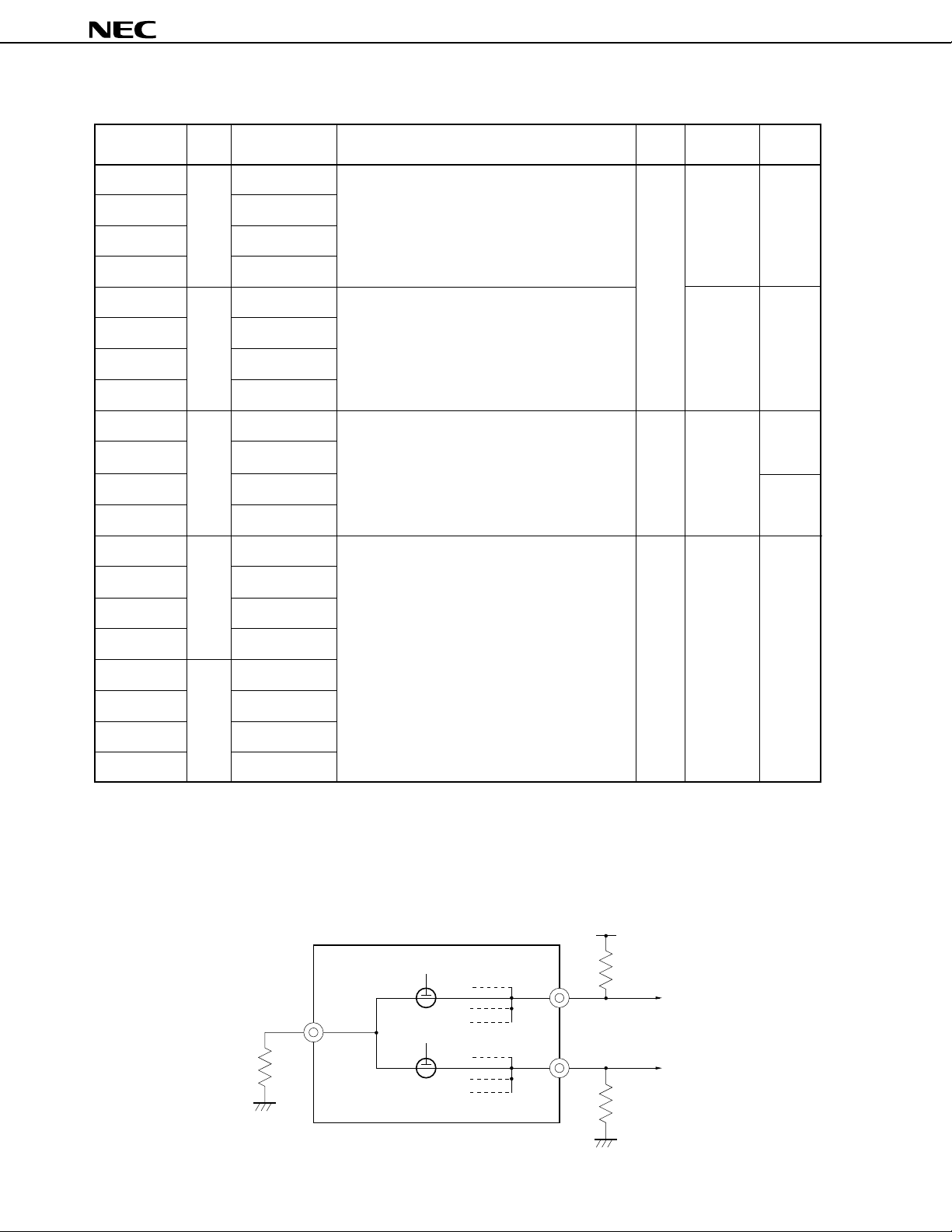
3. PIN FUNCTIONS
3.1 Port Pins (1/2)
µ
PD75P3036
Pin name I/O Alternate Function 8-bit Status I/O circuit
function I/O after reset type
P00 Input INT4 This is a 4-bit input port (PORT0). No Input <B>
Connection of an on-chip pull-up resistor can be
P01 I/O SCK specified in 3-bit units by software for P01 to P03. <F>-A
P02 I/O SO/SB0 <F>-B
P03 I/O SI/SB1 <M>-C
P10 Input INT0 This is a 4-bit input port (PORT1). No Input <B>-C
Connection of an on-chip pull-up resistor can be
P11 INT1 specified in 4-bit units by software.
P10/INT0 can select noise elimination circuit.
P12 INT2
P13 TI0
P20 I/O PTO0 This is a 4-bit I/O port (PORT2). No Input E-B
Connection of an on-chip pull-up resistor can be
P21 PTO1 specified in 4-bit units by software.
P22 PCL/PTO2
P23 BUZ
P30 I/O LCDCL/MD0 This is a programmable 4-bit I/O port (PORT3). No Input E-B
Input and output can be specified in bit units.
P31 SYNC/MD1 Connection of an on-chip pull-up resistor can be
specified in 4-bit units by software.
P32 MD2
Note 1
*
*
P33 MD3
Note 2
P40
P41
P42
P43
P50
P51
P52
P53
Note 2
Note 2
Note 2
Note 2
Note 2
Note 2
Note 2
I/O D0 This is an N-ch open-drain 4-bit I/O port (PORT4). Yes High M-E
When set to open-drain, voltage is 13 V. impedance
D1 Also functions as data I/O pin (lower 4 bits)
for program memory (PROM) write/verify.
D2
D3
I/O D4 This is an N-ch open-drain 4-bit I/O port (PORT5). High M-E
When set to open-drain, voltage is 13 V. impedance
D5 Also functions as data I/O pin (upper 4 bits)
for program memory (PROM) write/verify.
D6
D7
Notes 1. Circuit types enclosed in brackets indicate Schmitt trigger input.
2. Low level input leakage current increases when input instructions or bit manipulate instructions are executed.
7
Page 8
3.1 Port Pins (2/2)
µ
PD75P3036
Pin name I/O Alternate Function 8-bit Status I/O circuit
function I/O after reset type
P60 I/O KR0 This is a programmable 4-bit I/O port (PORT6). Yes Input <F>-A
Input and output can be specified in bit units.
P61 KR1 Connection of an on-chip pull-up resistor can be
specified in 4-bit units by software.
P62 KR2
P63 KR3
P70 I/O KR4 This is a 4-bit I/O port (PORT7). Input <F>-A
Connection of an on-chip pull-up resistor can be
P71 KR5 specified in 4-bit units by software.
P72 KR6
P73 KR7
P80 I/O TI1 This is a 4-bit I/O port (PORT8). No Input <E>-E
Connection of an on-chip pull-up resistor can be
P81 TI2 specified in 4-bit units by software.
P82 AN6 Y-B
P83 AN7
BP0 Output S24 These pins are also used as 1-bit I/O port (BIT No Note 2 H-A
PORT) segment output pin.
BP1 S25
Note 1
BP2 S26
BP3 S27
BP4 Output S28
BP5 S29
BP6 S30
BP7 S31
Notes 1. Circuit types enclosed in brackets indicate Schmitt trigger input.
LC1 as an input source.
*
2. BP0 through BP7 select V
However, the output levels change depending on the external circuit of BP0 through BP7 and V
Example Because BP0 through BP7 are mutually connected inside the
*
BP7 are determined by R
LC1
V
R
1
1, R2, and R3.
PD75P3036
µ
ON
ON
LC1.
µ
PD75P3036, the output levels of BP0 through
V
DD
R
2
BP0
BP1
R
3
8
Page 9
3.2 Non-port Pins (1/2)
µ
PD75P3036
Pin name I/O Alternate Function Status I/O circuit
function after reset type
TI0 Input P13 External event pulse input to timer/event counter Input <B>-C
TI1 P80 <E>-E
TI2 P81
PTO0 Output P20 Timer/event counter output Input E-B
PTO1 P21
PTO2 P22/PCL
PCL Output P22/PTO2 Clock output Input E-B
BUZ Output P23 Frequency output (for buzzer or system clock trimming) Input E-B
SCK I/O P01 Serial clock I/O Input <F>-A
SO/SB0 I/O P02 Serial data output Input <F>-B
Serial data bus I/O
SI/SB1 I/O P03 Serial data input Input <M>-C
Serial data bus I/O
INT4 Input P00 Edge detection vectored interrupt input Input <B>
(valid for detecting both rising and falling edges)
INT0 Input P10 Edge detection vectored interrupt input Noise elimination Input <B>-C
(detected edge is selectable) circuit
INT0/P10 can select noise elimination /asynchronous
circuit. is selectable
INT1 P11 Asynchronous
INT2 Input P12 Rising edge detection test input Asynchonous Input <B>-C
KR0 to KR3 Input P60 to P63 Parallel falling edge detection test input Input <F>-A
KR4 to KR7 Input P70 to P73 Parallel falling edge detection test input Input <F>-A
X1 Input — Ceramic/crystal oscillation circuit connection for main system — —
clock. If using an external clock, input to X1 and input
X2 — — inverted phase to X2.
XT1 Input — Crystal oscillation circuit connection for subsystem clock. — —
If using an external clock, input to XT1 and input inverted
XT2 — — phase to XT2.
RESET Input — System reset input (low level active) — <B>
MD0 I/O P30/LCDCL Mode selection for program memory (PROM) write/verify Input E-B
MD1 P31/SYNC
MD2, MD3 P32, P33
D0 to D3 I/O P40 to P43 Data bus for program memory (PROM) write/verify Input M-E
D4 to D7 P50 to P53
V
PP — — Programmable power supply voltage for program memory — —
(PROM) write/verify.
For normal operation, connect to VDD.
Apply +12.5 V for PROM write/verify.
V
DD — — Positive power supply — —
VSS — — Ground — —
XT1 can be used as a 1-bit (test) input.
Note
Note Circuit types enclosed in brackets indicate Schmitt trigger input.
9
Page 10
µ
PD75P3036
3.2 Non-port Pins (2/2)
Pin name I/O Alternate Function Status I/O circuit
function after reset type
S12 to S23 Output — Segment signal output Note 1 G-A
S24 to S31 Output BP0 to BP7 Segment signal output Note 1 H-A
COM0 to COM3
V
LC0 to VLC2 — — Power source for LCD driver — —
BIAS Output — Output for external split resistor cut High —
LCDCL
Note 2
SYNC
AN0 to AN5 Input — Analog signal input for A/D converter Input Y
AN6 P82 Y-B
AN7 P83
AV
REF — — A/D converter reference voltage — Z-N
AV
SS — — A/D converter reference GND potential — Z-N
Output — Common signal output Note 1 G-B
impedance
Note 2
Output P30/MD0 Clock output for driving external expansion driver Input E-B
Output P31/MD1 Clock output for synchronization of external expansion driver Input E-B
Notes 1. The VLCX (X = 0, 1, 2) shown below are selected as the input source for the display outputs.
S12 to S31: V
LC1, COM0 to COM2: VLC2, COM3: VLC0
2. These pins are provided for future system expansion. Currently, only P30 and P31 are used.
10
Page 11
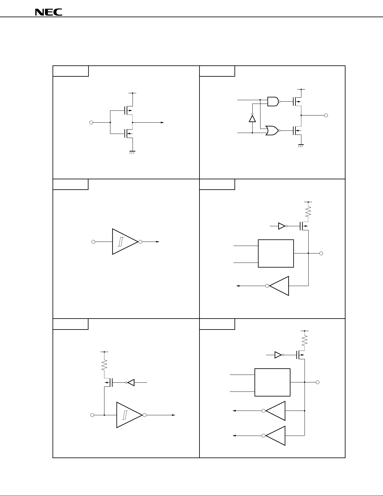
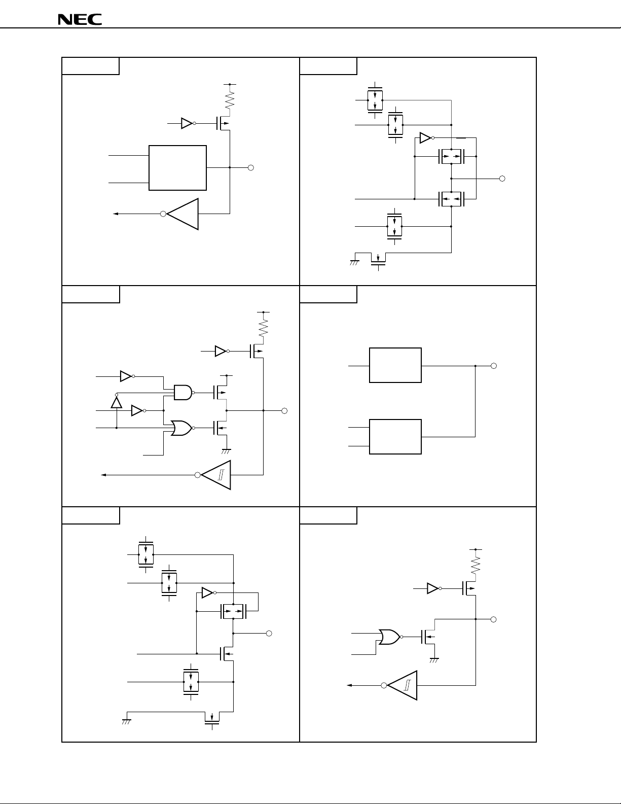
3.3 Pin Input/Output Circuits
µ
The input/output circuits for the
TYPE A TYPE D
PD75P3036’s pins are shown in schematic form below.
µ
PD75P3036
(1/3)
VDD
P-ch
IN
N-ch
CMOS standard input buffer
IN
VDD
data
output
disable
Push-pull output that can be set to output high-impedance
(with both P-ch and N-ch OFF).
TYPE E-BTYPE B
P.U.R.
enable
data
Type D
output
disable
P-ch
N-ch
VDD
P.U.R.
P-ch
IN/OUT
OUT
Schmitt trigger input with hysteresis characteristics.
TYPE B-C TYPE E-E
VDD
P.U.R.
data
output
disable
P-ch
IN
P.U.R. : Pull-Up Resistor
P.U.R.
enable
Type A
P.U.R. : Pull-Up Resistor
P.U.R.
enable
Type D
Type A
Type B
P.U.R. : Pull-Up Resistor
VDD
P.U.R.
P-ch
IN/OUT
11
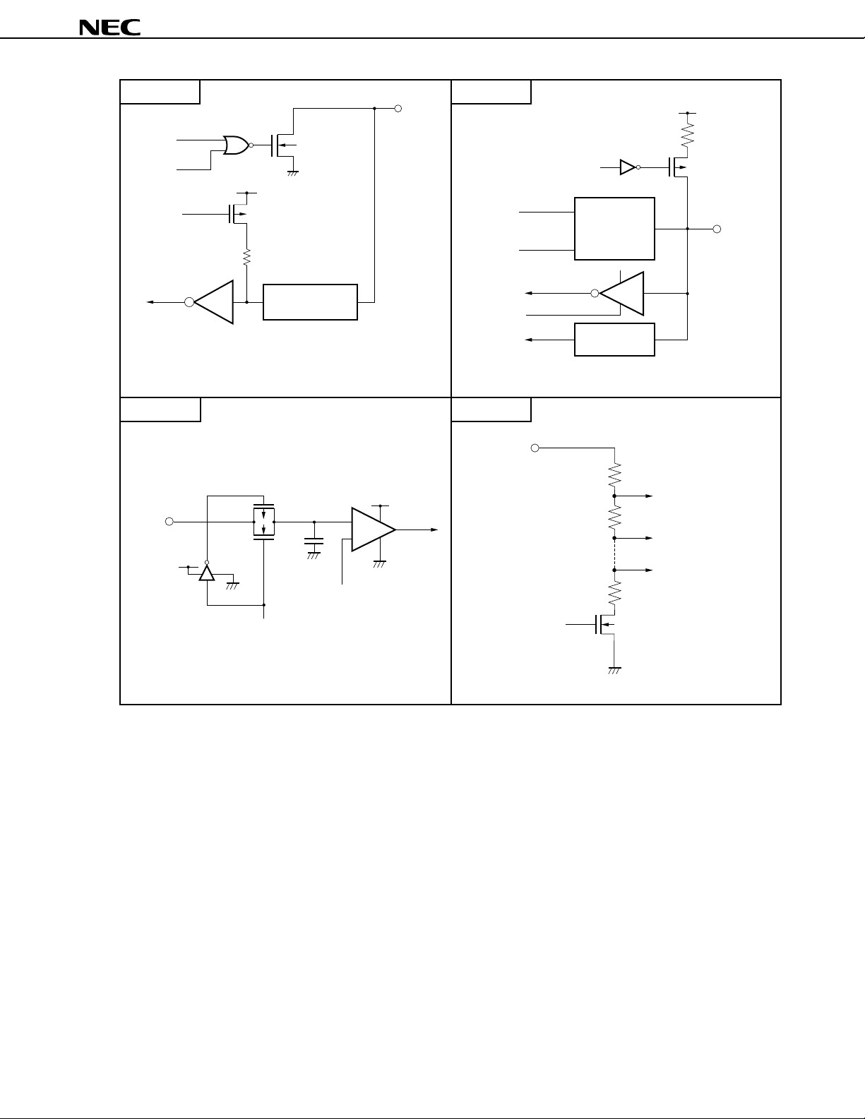
Page 12
TYPE F-A TYPE G-B
VDD
P.U.R.
µ
PD75P3036
(2/3)
*
V
LC0
output
disable
output
disable
(P)
data
output
disable
data
P.U.R.
enable
Type D
Type B
P.U.R. : Pull-Up Resistor
P.U.R.
enable
output
disable
(N)
VDD
P-ch
P-ch
N-ch
IN/OUT
VDD
P.U.R.
P-ch
IN/OUT
VLC1
COM or SEG
TYPE H-ATYPE F-B
V
SEG
data
Bit Port
data
output
disable
data
LC2
*
N-ch
Type G-A
Type E-B
P-ch
N-ch
N-ch
OUT
P-ch
IN/OUT
P.U.R. : Pull-Up Resistor
TYPE G-A TYPE M-C
*
LC0
V
VLC1
SEG
data
V
LC2
N-chP-ch
OUT
N-ch
N-ch
12
data
output
disable
P.U.R.
enable
N-ch
P.U.R. : Pull-Up Resistor
VDD
P.U.R.
P-ch
IN/OUT
Page 13
TYPE M-E TYPE Y-B
*
IN/OUT
µ
PD75P3036
VDD
(3/3)
data
output
disable
input
instruction
Note
IN
N-ch
(+13 V
withstand
V
DD
P-ch
P.U.R.
The pull-up resistor operates only when an input
instruction is executed (current flows from V
the pin when the pin is low).
P-ch
N-ch
V
DD
SS
AV
input
enable
voltage)
Note
Voltage limitation
circuit
Sampling C
reference voltage
(from voltage tap of
series resistor string)
(+13 V withstand
voltage)
DD to
VDD
+
–
AVSS
TYPE Z-NTYPE Y
data
output
disable
Note
port
input
P.U.R. : Pull-Up Resistor
*
AVREF
P.U.R.
enable
Type D
Type A
Type Y
N-chADEN
P-ch
IN/OUT
reference
voltage
Note Becomes active when an input instruction is executed.
AVSS
13
Page 14
3.4 Recommended Connection of Unused Pins
*
Pin Recommended connection
P00/INT4 Connect to VSS or VDD
P01/SCK Connect to VSS or VDD via a resistor individually
P02/SO/SB0
P03/SI/SB1 Connect to V
P10/INT0 to P12/INT2
P13/TI0
P20/PTO0 Input status : connect to V
P21/PTO1 Output status: open
P22/PTO2/PCL
P23/BUZ
P30/LCDCL
P31/SYNC
P32, P33
P40 to P43 Connect to V
P50 to P53
P60/KR0 to P63/KR3
P70/KR4 to P73/KR7
P80/TI1
P81/TI2
P82/AN6
P83/AN7
S12 to S23 Open
S24/BP0 to S31/BP7
COM0 to COM3
V
LC0 to VLC2 Connect to VSS
BIAS Connect to VSS only when VLC0 to VLC2 are all not used.
Note
XT1
Note
XT2
AN0 to AN5 Connect to V
VPP Connect to VDD directly
Connect to VSS or VDD
Input status : connect to VSS or VDD via a resistor individually.
Output status: open
In other cases, leave open.
Connect to VSS or VDD
Open
SS
SS
SS or VDD
SS or VDD via a resistor individually.
µ
PD75P3036
14
Note When the subsystem clock is not used, set SOS.0 to 1 (so as not to use
the internal feedback resistor).
Page 15
µ
PD75P3036
4. Mk I MODE AND Mk II MODE SELECTION FUNCTION
Setting a stack bank selection (SBS) register for the µPD75P3036 enables the program memory to be switched between
µ
Mk I mode and Mk II mode. This function is applicable when using the
PD75P3036 to evaluate the µPD753036.
When the SBS bit 3 is set to 1 : sets Mk I mode (supports Mk I mode for
When the SBS bit 3 is set to 0 : sets Mk II mode (supports Mk II mode for
4.1 Difference between Mk I Mode and Mk II Mode
Table 4-1 lists points of difference between the Mk I mode and the Mk II mode for the
Table 4-1. Difference between Mk I Mode and Mk II Mode
Item Mk I Mode Mk II Mode
Program counter PC
Program memory (bytes) 16384
Data memory (bits) 768 x 4
Stack Stack bank Selectable via memory banks 0 to 2
No. of stack bytes 2 bytes 3 bytes
Instruction BRA !addr1 instruction Not available Available
CALLA !addr1 instruction
Instruction CALL !addr instruction 3 machine cycles 4 machine cycles
execution time CALLF !faddr instruction 2 machine cycles 3 machine cycles
Supported mask ROM versions When set to Mk I mode for
13-0
µ
µ
PD753036)
µ
PD753036)
µ
PD75P3036.
PD753036 When set to Mk II mode for µPD753036
*
Caution The Mk II mode supports a program area exceeding 16 Kbytes for the 75X and 75XL series.
Therefore, this mode is effective for enhancing software compatibility with products exceeding 16
Kbytes.
When the Mk II mode is selected, the number of stack bytes used during execution of subroutine
call instructions increases by one byte per stack compared to the Mk I mode. When the CALL !addr
and CALLF !faddr instructions are used, the machine cycle becomes longer by one machine cycle.
Therefore, use the Mk I mode if the RAM efficiency and processing performance are more important
than software compatibility.
15
Page 16
µ
PD75P3036
4.2 Setting of Stack Bank Selection Register (SBS)
Use the stack bank selection register to switch between Mk I mode and Mk II mode. Figure 4-1 shows the format for doing
this.
The stack bank selection register is set using a 4-bit memory manipulation instruction. When using the Mk I mode, be
Note
sure to initialize the stack bank selection register to 10xxB
Note
be sure to initialize it to 00xxB
.
at the beginning of the program. When using the Mk II mode,
Note Set the desired value for xx.
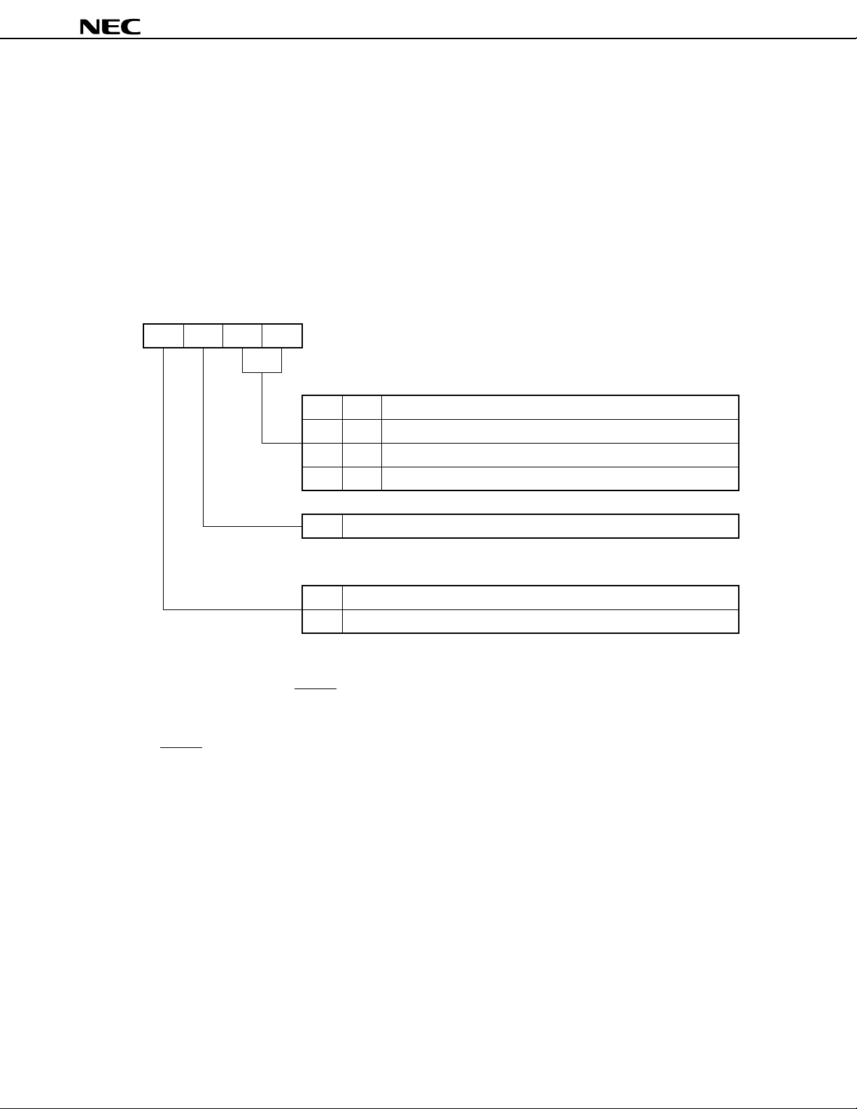
Figure 4-1. Format of Stack Bank Selection Register
Address 3 2 1 0
SBS3 SBS2 SBS1 SBS0F84H
Symbol
SBS
Stack area specification
0
0
Memory bank 0
0
1
Memory bank 1
1
0
Memory bank 2
1
1
Setting prohibited
0 Be sure to enter “0” for bit 2.
Mode selection specification
01Mk II mode
Mk I mode
Cautions 1. SBS3 is set to “1” after RESET input, and consequently the CPU operates in Mk I mode. When using
instructions for Mk II mode, set SBS3 to “0” and set Mk II mode before using the instructions.
2. When using Mk II mode, execute a subroutine call instruction and an interrupt instruction after
RESET input and after setting the stack bank selection register.
16
Page 17
µ
PD75P3036
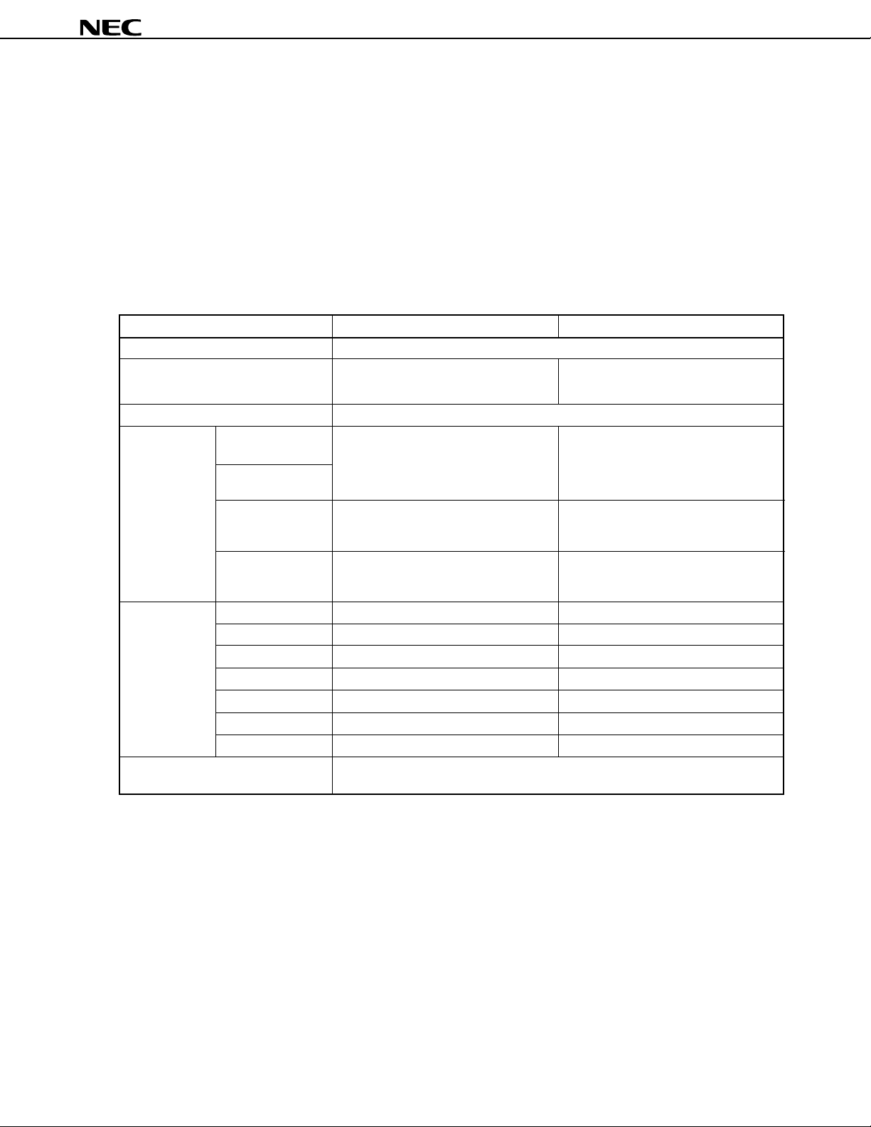
5. DIFFERENCES BETWEEN µPD75P3036 AND µPD753036
The µPD75P3036 replaces the internal mask ROM in the program memory of the µPD753036 with a one-time PROM or
µ
EPROM. The
supports the Mk II mode in the
Table 5-1 lists differences among the
products before using them with PROMs for debugging or prototype testing of application systems or, later, when using
them with a mask ROM for full-scale production.
As to CPU function and on-chip hardware, see the User’s Manual.
PD75P3036’s Mk I mode supports the Mk I mode in the µPD753036 and the µPD75P3036’s Mk II mode
µ
PD753036.
µ
PD75P3036 and the µPD753036. Be sure to check the differences among these
µ
Table 5-1. Differences between
PD75P3036 and µPD753036
Item
Program counter 14 bits
Program memory (bytes) 16384 16384
Mask ROM One-time PROM, EPROM
Data memory (x 4 bits) 768
Mask option Pull-up resistor of Yes (can specify whether to incorporate No (don’t incorporate on-chip)
ports 4, 5 on-chip or not)
Split resistor for LCD
driving power supply
Selection of Yes (can select either 2
oscillation
stabilization wait time
Selection of Yes (can select either use enabled or use No (use enabled)
subsystem clock disabled)
feedback resistor
Pin configuration Pin No. 29 to 32 P40 to P43 P40/D0 to P43/D3
Pin No. 34 to 37 P50 to P53 P50/D4 to P53/D7
Pin No. 50 P30/LCDCL P30/LCDCL/MD0
Pin No. 51 P31/SYNC P31/SYNC/MD1
Pin No. 52 P32 P32/MD2
Pin No. 53 P33 P33/MD3
Pin No. 69 IC V
Other Noise resistance and noise radiation may differ due to the different circuit sizes and mask
layouts.
µ
PD753036
17
/fX or 215/fX)
Note
µ
No (fixed to 215/fX)
PP
PD75P3036
Note
Note 217/fX is 21.8 ms during 6.0-MHz operation, and 31.3 ms during 4.19-MHz operation.
15
/fX is 5.46 ms during 6.0-MHz operation, and 7.81 ms during 4.19-MHz operation.
2
Caution Noise resistance and noise radiation are different in PROM and mask ROM versions. In transferring to
mask ROM versions from the PROM version in a process between prototype development and full
production, be sure to fully evaluate the mask ROM version’s CS (not ES).
17
Page 18

µ
PD75P3036
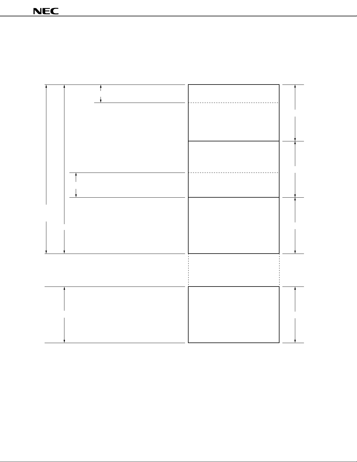
6. PROGRAM COUNTER (PC) AND MEMORY MAP
6.1 Program Counter (PC) ... 14 bits
This is a 14-bit binary counter that stores program memory address data.
Figure 6-1. Configuration of Program Counter
PC13 PC12 PC11 PC10 PC9 PC8 PC7 PC6 PC5 PC4 PC3 PC2 PC1 PC0 PC
6.2 Program Memory (PROM) ... 16384 x 8 bits
The program memory consists of 16384 x 8-bit one-time PROM or EPROM.
• Addresses 0000H and 0001H
Vector table wherein the program start address and the values set for the RBE and MBE at the time a RESET signal is
generated are written. Reset start is possible from any address.
• Addresses 0002H to 000DH
Vector table wherein the program start address and the values set for the RBE and MBE by each vectored interrupt are
written. Interrupt processing can start from any address.
• Addresses 0020H to 007FH
Note
Table area referenced by the GETI instruction
Note The GETI instruction realizes a 1-byte instruction on behalf of any 2-byte/3-byte instruction, or two 1-byte
instructions. It is used to decrease the number of program steps.
.
18
Page 19

µ
PD75P3036
Figure 6-2 shows the addressing ranges for the program memory, branch instruction and the subroutine call instruction.
Figure 6-2. Program Memory Map
765 0
MBE
RBE
0000H
0002H
0004H
0006H
0008H
000AH
MBE
MBE
MBE
MBE
MBE
Internal reset start address (upper 6 bits)
Internal reset start address (lower 8 bits)
RBE
INTBT/INT4 start address (upper 6 bits)
INTBT/INT4 start address (lower 8 bits)
RBE
INT0 start address (upper 6 bits)
INT0 start address (lower 8 bits)
RBE
INT1 start address (upper 6 bits)
INT1 start address (lower 8 bits)
RBE
INTCSI start address (upper 6 bits)
INTCSI start address (lower 8 bits)
RBE
INTT0 start address (upper 6 bits)
CALLF
!faddr instruction
entry address
!caddr instruction
BRCB
branch address
Branch address
for the following
instructions
• BR BCXA
• BR BCDE
• BR !addr
• BRA !addr1
• CALLA !addr1
Note
Note
000CH
0020H
007FH
0080H
07FFH
0800H
0FFFH
1000H
1FFFH
2000H
2FFFH
3000H
3FFFH
MBE
INTT0 start address (lower 8 bits)
RBE
INTT1, INTT2 start address (upper 6 bits)
INTT1, INTT2 start address (lower 8 bits)
Reference table for GETI instruction
CALL !addr instruction
BR $addr instruction
relative branch address
BRCB
!caddr instruction
branch address
BRCB
!caddr instruction
branch address
BRCB
!caddr instruction
branch address
subroutine
entry address
Branch/call
address
by GETI
(–15 to –1,
+2 to +16)
*
Note Can be used only in the Mk II mode.
Remark For instructions other than those noted above, the BR PCDE and BR PCXA instructions can be used to branch
to addresses with changes in the PC’s lower 8 bits only.
19
Page 20
µ
PD75P3036
6.3 Data Memory (RAM) ... 768 x 4 bits
Figure 6-3 shows the data memory configuration.
Data memory consists of a data area and a peripheral hardware area. The data area consists of 768 x 4-bit static RAM.
Figure 6-3. Data Memory Map
Data area
static RAM
(768 x 4)
Display data memory
Stack area
Note
General-purpose register area
Data memory
000H
(32 x 4)
01FH
020H
256 x 4
(224 x 4)
0FFH
100H
256 x 4
(236 x 4)
1EBH
1ECH
(20 x 4)
1FFH
200H
256 x 4
Memory bank
0
1
2
2FFH
F80H
Peripheral hardware area
FFFH
Note Memory bank 0, 1, or 2 can be selected as the stack area.
Not incorporated
128 x 4
15
20
Page 21

µ
PD75P3036
7. INSTRUCTION SET
(1) Representation and coding formats for operands
In the instruction’s operand area, use the following coding format to describe operands corresponding to the instruction’s
operand representations (for further description, see the RA75X Assembler Package User’s Manual—Language
(EEU-1363)). When there are several codes, select and use just one. Codes that consist of uppercase letters and + or
– symbols are key words that should be entered as they are.
For immediate data, enter an appropriate numerical value or label.
Enter register flag symbols as label descriptors instead of mem, fmem, pmem, bit, etc. (for further description, see the
User’s Manual). The number of labels that can be entered for fmem and pmem are restricted.
Representation Coding format
reg X, A, B, C, D, E, H, L
reg1 X, B, C, D, E, H, L
rp XA, BC, DE, HL
rp1 BC, DE, HL
rp2 BC, DE
rp’ XA, BC, DE, HL, XA’, BC’, DE’, HL’
rp’1 BC, DE, HL, XA’, BC’, DE’, HL’
rpa HL, HL+, HL–, DE, DL
rpa1 DE, DL
n4 4-bit immediate data or label
n8 8-bit immediate data or label
mem 8-bit immediate data or label
bit 2-bit immediate data or label
fmem FB0H-FBFH, FF0H-FFFH immediate data or label
pmem FC0H-FFFH immediate data or label
addr 0000H-3FFFH immediate data or label
addr1 0000H-3FFFH immediate data or label
caddr 12-bit immediate data or label
faddr 11-bit immediate data or label
taddr 20H-7FH immediate data (however, bit0 = 0) or label
PORTn PORT0-PORT8
IEXXX IEBT, IECSI, IET0-IET2, IE0-IE2, IE4, IEW
RBn RB0-RB3
MBn MB0-MB2, MB15
Note
Note When processing 8-bit data, only even-numbered addresses can be entered.
21
Page 22

(2) Operation legend
A : A register; 4-bit accumulator
B : B register
C : C register
D : D register
E : E register
H : H register
L : L register
X : X register
XA : Register pair (XA); 8-bit accumulator
BC : Register pair (BC)
DE : Register pair (DE)
HL : Register pair (HL)
XA’ : Expansion register pair (XA’)
BC’ : Expansion register pair (BC’)
DE’ : Expansion register pair (DE’)
HL’ : Expansion register pair (HL’)
PC : Program counter
SP : Stack pointer
CY : Carry flag; bit accumulator
PSW : Program status word
MBE : Memory bank enable flag
RBE : Register bank enable flag
PORTn : Port n (n = 0 to 8)
IME : Interrupt master enable flag
IPS : Interrupt priority selection register
IEXXX : Interrupt enable flag
RBS : Register bank selection register
MBS : Memory bank selection register
PCC : Processor clock control register
. : Delimiter for address and bit
(XX) : The contents addressed by XX
XXH : Hexadecimal data
µ
PD75P3036
22
Page 23

(3) Description of symbols used in addressing area
MB = MBE • MBS
*1
MB = 0
*2
MBE = 0 :
*3
MBE = 1 :
MB = 15, fmem = FB0H-FBFH, FF0H-FFFH
*4
MB = 15, pmem = FC0H-FFFH
*5
addr = 0000H-3FFFH
*6
addr, addr1 =*7(Current PC) –15 to (Current PC) –1
caddr =0000H-0FFFH (PC
*8
MBS = 0-2, 15
MB = 0 (000H-07FH)
MB = 15 (F80H-FFFH)
MB = MBS
MBS = 0-2, 15
(Current PC) +2 to (Current PC) +16
13, 12 = 00B: Mk I or Mk II mode) or
1000H-1FFFH (PC13, 12 = 01B: Mk I or Mk II mode) or
2000H-2FFFH (PC13, 12 = 10B: Mk I or Mk II mode) or
3000H-3FFFH (PC13, 12 = 11B: Mk I or Mk II mode)
µ
PD75P3036
Data memory
addressing
Program memory
addressing
faddr = 0000H-07FFH
*9
taddr = 0020H-007FH
*10
addr1 = 0000H-3FFFH
*11
Remarks 1. MB indicates access-enabled memory banks.
2. In area *2, MB = 0 for both MBE and MBS.
3. In areas *4 and *5, MB = 15 for both MBE and MBS.
4. Areas *6 to *11 indicate corresponding address-enabled areas.
(4) Description of machine cycles
S indicates the number of machine cycles required for skipping of skip-specified instructions. The value of S varies as
shown below.
• No skip .....................................................................S = 0
• Skipped instruction is 1-byte or 2-byte instruction.... S = 1
Note
• Skipped instruction is 3-byte instruction
..............S = 2
Note 3-byte instructions: BR !addr, BRA !addr1, CALL !addr, CALLA !addr1
Caution The GETI instruction is skipped for one machine cycle.
One machine cycle equals one cycle (= t
CY) of the CPU clock Φ. Use the PCC setting to select among four cycle times.
23
Page 24

µ
PD75P3036
Instruction Mnemonic Operand
group
Transfer MOV A, #n4 1 1 A<-n4 String-effect A
reg1, #n4 2 2 reg1<-n4
XA, #n8 2 2 XA<-n8 String-effect A
HL, #n8 2 2 HL<-n8 String-effect B
rp2, #n8 2 2 rp2<-n8
A, @HL 1 1 A<-(HL) *1
A, @HL+ 1 2+S A<-(HL), then L<-L+1 *1 L=0
A, @HL– 1 2+S A<-(HL), then L<-L–1 *1 L=FH
A, @rpa1 1 1 A<-(rpa1) *2
XA, @HL 2 2 XA<-(HL) *1
@HL, A 1 1 (HL)<-A *1
@HL, XA 2 2 (HL)<-XA *1
A, mem 2 2 A<-(mem) *3
XA, mem 2 2 XA<-(mem) *3
mem, A 2 2 (mem)<-A *3
mem, XA 2 2 (mem)<-XA *3
A, reg1 2 2 A<-reg1
XA, rp’ 2 2 XA<-rp’
reg1, A 2 2 reg1<-A
rp’1, XA 2 2 rp’1<-XA
XCH A, @HL 1 1 A<->(HL) *1
A, @HL+ 1 2+S A<->(HL), then L<-L+1 *1 L=0
A, @HL– 1 2+S A<->(HL), then L<-L–1 *1 L=FH
A, @rpa1 1 1 A<->(rpa1) *2
XA, @HL 2 2 XA<->(HL) *1
A, mem 2 2 A<->(mem) *3
XA, mem 2 2 XA<->(mem) *3
A, reg1 1 1 A<->reg1
XA, rp’ 2 2 XA<->rp’
Table MOVT XA, @PCDE 1 3 XA<-(PC
reference XA, @PCXA 1 3 XA<-(PC13-8+XA)ROM
XA, @BCDE 1 3 XA<-(BCDE)ROM
XA, @BCXA 1 3 XA<-(BCXA)ROM
No. of Machine
bytes cycle area
Operation
13-8+DE)ROM
Note
Note
Addressing
*6
*6
Skip
condition
Note Only the lower 2 bits in the B register are valid.
24
Page 25

µ
PD75P3036
Instruction Mnemonic Operand
group
Bit transfer MOV1 CY, fmem.bit 2 2 CY<-(fmem.bit) *4
CY, pmem.@L 2 2 CY<-(pmem
CY, @H+mem.bit 2 2 CY<-(H+mem
fmem.bit, CY 2 2 (fmem.bit)<-CY *4
pmem.@L, CY 2 2 (pmem
@H+mem.bit, CY 2 2 (H+mem
Arithmetic/ ADDS A, #n4 1 1+S A<-A+n4 carry
logical XA, #n8 2 2+S XA<-XA+n8 carry
operation A, @HL 1 1+S A<-A+(HL) *1 carry
XA, rp’ 2 2+S XA<-XA+rp’ carry
rp’1, XA 2 2+S rp’1<-rp’1+XA carry
ADDC A, @HL 1 1 A, CY<-A+(HL)+CY *1
XA, rp’ 2 2 XA, CY<-XA+rp’+CY
rp’1, XA 2 2 rp’1, CY<-rp’1+XA+CY
SUBS A, @HL 1 1+S A<-A–(HL) *1 borrow
XA, rp’ 2 2+S XA<-XA–rp’ borrow
rp’1, XA 2 2+S rp’1<-rp’1–XA borrow
SUBC A, @HL 1 1 A, CY<-A–(HL)–CY *1
XA, rp’ 2 2 XA, CY<-XA–rp’–CY
rp’1, XA 2 2 rp’1, CY<-rp’1–XA–CY
AND A, #n4 2 2 A<-A
A, @HL 1 1 A<-A
XA, rp’ 2 2 XA<-XA
rp’1, XA 2 2 rp’1<-rp’1^XA
OR A, #n4 2 2 A<-Avn4
A, @HL 1 1 A<-Av(HL) *1
XA, rp’ 2 2 XA<-XAvrp’
rp’1, XA 2 2 rp’1<-rp’1vXA
XOR A, #n4 2 2 A<-Av
A, @HL 1 1 A<-Av
XA, rp’ 2 2 XA<-XAvrp’
rp’1, XA 2 2 rp’1<-rp’1v
Accumulator RORC A 1 1 CY<-A
manipulation NOT A 2 2 A<-A
Increment/ INCS reg 1 1+S reg<-reg+1 reg=0
decrement rp1 1 1+S rp1<-rp1+1 rp1=00H
@HL 2 2+S (HL)<-(HL)+1 *1 (HL)=0
mem 2 2+S (mem)<-(mem)+1 *3 (mem)=0
DECS reg 1 1+S reg<-reg–1 reg=FH
rp’ 2 2+S rp’<-rp’–1 rp’=FFH
No. of Machine
bytes cycle area
n4
^
(HL) *1
^
n4
(HL) *1
Operation
7-2+L3-2.bit(L1-0)) *5
3-0.bit) *1
7-2+L3-2.bit(L1-0))<-CY *5
3-0.bit)<-CY *1
rp’
^
XA
0, A3<-CY, An–1<-An
Addressing
Skip
condition
25
Page 26

µ
PD75P3036
Instruction Mnemonic Operand
group
No. of Machine
Operation
Addressing
bytes cycle area
condition
Comparison SKE reg, #n4 2 2+S Skip if reg=n4 reg=n4
@HL, #n4 2 2+S Skip if(HL)=n4 *1 (HL)=n4
A, @HL 1 1+S Skip if A=(HL) *1 A=(HL)
XA, @HL 2 2+S Skip if XA=(HL) *1 XA=(HL)
A, reg 2 2+S Skip if A=reg A=reg
XA, rp’ 2 2+S Skip if XA=rp’ XA=rp’
Carry flag SET1 CY 1 1 CY<-1
manipulation CLR1 CY 1 1 CY<-0
SKT CY 1 1+S Skip if CY=1 CY=1
NOT1 CY 1 1 CY<-CY
Memory bit SET1 mem.bit 2 2 (mem.bit)<-1 *3
manipulation fmem.bit 2 2 (fmem.bit)<-1 *4
pmem.@L 2 2 (pmem
@H+mem.bit 2 2 (H+mem
7-2+L3-2.bit(L1-0))<-1 *5
3-0.bit)<-1 *1
CLR1 mem.bit 2 2 (mem.bit)<-0 *3
fmem.bit 2 2 (fmem.bit)<-0 *4
pmem.@L 2 2 (pmem
7-2+L3-2.bit(L1-0))<-0 *5
@H+mem.bit 2 2 (H+mem3-0.bit)<-0 *1
SKT mem.bit 2 2+S Skip if(mem.bit)=1 *3 (mem.bit)=1
fmem.bit 2 2+S Skip if(fmem.bit)=1 *4 (fmem.bit)=1
pmem.@L 2 2+S Skip if(pmem
@H+mem.bit 2 2+S Skip if(H+mem
7-2+L3-2.bit(L1-0))=1 *5 (pmem.@L)=1
3-0.bit)=1 *1
(@H+mem.bit)=1
SKF mem.bit 2 2+S Skip if(mem.bit)=0 *3 (mem.bit)=0
fmem.bit 2 2+S Skip if(fmem.bit)=0 *4 (fmem.bit)=0
pmem.@L 2 2+S Skip if(pmem
@H+mem.bit 2 2+S Skip if(H+mem
7-2+L3-2.bit(L1-0))=0 *5 (pmem.@L)=0
3-0.bit)=0 *1
(@H+mem.bit)=0
SKTCLR fmem.bit 2 2+S Skip if(fmem.bit)=1 and clear *4 (fmem.bit)=1
pmem.@L 2 2+S
@H+mem.bit 2 2+S Skip if(H+mem
Skip if(pmem7-2+L3-2.bit (L1-0))=1 and clear
3-0.bit)=1 and clear *1
*5 (pmem.@L)=1
(@H+mem.bit)=1
AND1 CY, fmem.bit 2 2 CY<-CY^(fmem.bit) *4
CY, pmem.@L 2 2 CY<-CY^(pmem7-2+L3-2.bit(L1-0)) *5
CY, @H+mem.bit 2 2 CY<-CY
(H+mem3-0.bit) *1
^
OR1 CY, fmem.bit 2 2 CY<-CYv(fmem.bit) *4
CY, pmem.@L 2 2 CY<-CYv(pmem
CY, @H+mem.bit 2 2 CY<-CYv(H+mem
XOR1 CY, fmem.bit 2 2 CY<-CYv
CY, pmem.@L 2 2 CY<- CYv
7-2+L3-2.bit(L1-0)) *5
3-0.bit) *1
(fmem.bit) *4
(pmem7-2+L3-2.bit(L1-0)) *5
CY, @H+mem.bit 2 2 CY<-CYv(H+mem3-0.bit) *1
Skip
26
Page 27

µ
PD75P3036
Instruction Mnemonic Operand
group
Branch BR
Note 1
addr — — PC13-0<-addr *6
addr1 — — PC
!addr 3 3 PC13-0<-addr *6
$addr 1 2 PC
$addr1 1 2 PC
PCDE 2 3 PC13-0<-PC13-8+DE
PCXA 2 3 PC
BCDE 2 3 PC
BCXA 2 3 PC
Note 1
BRA
!addr1 3 3 PC13-0<-addr1 *11
BRCB !caddr 2 2 PC
No. of Machine
Operation
Addressing
bytes cycle area
Use the assembler to select the
most appropriate instruction
among the following.
• BR !addr
• BRCB !caddr
• BR $addr
13-0<-addr1 *11
Use the assembler to select
the most appropriate instruction
among the following.
• BRA !addr1
• BR !addr
• BRCB !caddr
• BR $addr1
13-0<-addr *7
13-0<-addr1
13-0<-PC13-8+XA
13-0<-BCDE
13-0<-BCXA
13-0<-PC13, 12+caddr11-0 *8
Note 2
Note 2
*6
*6
Skip
condition
Notes 1. The above operations in the double boxes can be performed only in the Mk II mode. The other operations can
be performed only in the Mk I mode.
2. Only the lower 2 bits in the B register are valid.
27
Page 28

µ
PD75P3036
Instruction Mnemonic Operand
group
Subroutine CALLA
Note
!addr1 3 3 (SP–6)(SP–3)(SP–4)<-PC11-0 *11
No. of Machine
Operation
bytes cycle area
stack control (SP–5)<-0, 0, PC
(SP–2)<-X, X, MBE, RBE
PC
13–0<-addr1, SP<-SP–6
Note
CALL
!addr 3 3 (SP–4)(SP–1)(SP–2)<-PC11-0 *6
(SP–3)<-MBE, RBE, PC
PC13–0<-addr, SP<-SP–4
4 (SP–6)(SP–3)(SP–4)<-PC
(SP–5)<-0, 0, PC13, 12
(SP–2)<-X, X, MBE, RBE
PC
13-0<-addr, SP<-SP–6
Note
CALLF
!faddr 2 2 (SP–4)(SP–1)(SP–2)<-PC11-0 *9
(SP–3)<-MBE, RBE, PC13, 12
PC13-0<-000+faddr, SP<-SP–4
3 (SP–6)(SP–3)(SP–4)<-PC
(SP–5)<-0, 0, PC13, 12
(SP–2)<-X, X, MBE, RBE
PC
13-0<-000+faddr, SP<-SP–6
Note
RET
1 3 MBE, RBE, PC13, 12<-(SP+1)
PC11-0<-(SP)(SP+3)(SP+2)
SP<-SP+4
X, X, MBE, RBE<-(SP+4)
PC
11-0<-(SP)(SP+3)(SP+2)
0, 0, PC
13, 12<-(SP+1)
SP<-SP+6
Note
RETS
1 3+S MBE, RBE, PC13, 12<-(SP+1) Unconditional
PC
11-0<-(SP)(SP+3)(SP+2)
SP<-SP+4
then skip unconditionally
X, X, MBE, RBE<-(SP+4)
PC
11-0<-(SP)(SP+3)(SP+2)
0, 0, PC
13, 12<-(SP+1)
SP<-SP+6
then skip unconditionally
Note
RETI
1 3 MBE, RBE, PC13, 12<-(SP+1)
PC11-0<-(SP)(SP+3)(SP+2)
PSW<-(SP+4)(SP+5), SP<-SP+6
0, 0, PC
13, 12<-(SP+1)
PC
11-0<-(SP)(SP+3)(SP+2)
PSW<-(SP+4)(SP+5), SP<-SP+6
13, 12
13, 12
11-0
11-0
Addressing
Skip
condition
Note The above operations in the double boxes can be performed only in the Mk II mode. The other operations can be
performed only in the Mk I mode.
28
Page 29

µ
PD75P3036
Instruction Mnemonic Operand
group
No. of Machine
Operation
bytes cycle area
Subroutine PUSH rp 1 1 (SP–1)(SP–2)<-rp, SP<-SP–2
stack control BS 2 2
(SP–1)<-MBS, (SP–2)<-RBS, SP<-SP–2
POP rp 1 1 rp<-(SP+1)(SP), SP<-SP+2
BS 2 2 MBS<-(SP+1), RBS<-(SP), SP<-SP+2
Interrupt EI 2 2 IME(IPS.3)<-1
control IEXXX 2 2 IEXXX<-1
DI 2 2 IME(IPS.3)<-0
IEXXX 2 2 IEXXX<-0
I/O IN
Note 1
OUT
A, PORTn 2 2 A<-PORTn (n=0-8)
XA, PORTn 2 2 XA<-PORTn+
Note 1
PORTn, A 2 2 PORTn<-A (n=2-8)
PORTn, XA 2 2 PORTn+
1, PORTn (n=4, 6)
1, PORTn<-XA (n=4, 6)
CPU control HALT 2 2 Set HALT Mode(PCC.2<-1)
STOP 2 2 Set STOP Mode(PCC.3<-1) *10
NOP 1 1 No Operation
Special SEL RBn 2 2 RBS<-n (n=0-3)
MBn 2 2 MBS<-n (n=0-2, 15)
Note 2, 3
GETI
taddr 1 3 • When using TBR instruction
PC
13-0<-(taddr)5-0+(taddr+1)
- - - - - - - - - - - - - - - - - - - - - - - - - - -
• When using TCALL instruction
(SP–4)(SP–1)(SP–2)<-PC
(SP–3)<-MBE, RBE, PC13, 12
11-0
PC13-0<-(taddr)5-0+(taddr+1)
SP<-SP–4
- - - - - - - - - - - - - - - - - - - - - - - - - - -
• When using instruction other than Determined by
TBR or TCALL referenced
Execute (taddr)(taddr+1) instruction instruction
1 3 • When using TBR instruction *10
PC
- - - - - - - - - - - - - - - - - - - - - - - - - - - - - - - -
13-0<-(taddr)5-0+(taddr+1)
4 • When using TCALL instruction
(SP–6)(SP–3)(SP–4)<-PC
11-0
(SP–5)<-MBE, RBE, PC13, 12
(SP–2)<-X, X, MBE, RBE
PC
13-0<-(taddr)5-0+(taddr+1)
- - - - - - - - - - - - - - - - - - - - - - - - - - - - - - - -
SP<-SP–6
3 • When using instruction other than Determined by
TBR or TCALL referenced
Execute (taddr)(taddr+1) instruction instruction
Addressing
Skip
condition
- - - - - - - - - - - -
- - - - - - - - - - - -
- - - - - - - - - - - -
- - - - - - - - - - - -
Notes 1. Before executing the IN or OUT instruction, set MBE to 0 or 1 and set MBS to 15.
2. TBR and TCALL instructions are assembler pseudo-instructions for the GETI instruction’s table definitions.
3. The above operations in the double boxes can be performed only in the Mk II mode. The other operations can
be performed only in the Mk I mode.
29
Page 30

µ
PD75P3036
8. PROM (PROGRAM MEMORY) WRITE AND VERIFY
The µPD75P3036 contains a 16384 x 8-bit PROM as a program memory. The pins listed in the table below are used for
this PROM’s write/verify operations. Clock input from the X1 pin is used instead of address input as a method for updating
addresses.
Pin Function
VPP Pin where program voltage is applied during program memory
write/verify (usually VDD potential)
X1, X2 Clock input pins for address updating during program memory
write/verify. Input the X1 pin’s inverted signal to the
X2 pin.
MD0 to MD3 Operation mode selection pin for program memory write/verify
D0/P40 to D3/P43 8-bit data I/O pins for program memory write/verify
(lower 4 bits)
D4/P50 to D7/P53
(upper 4 bits)
V
DD Pin where power supply voltage is applied. Applies 1.8 to 5.5
V in normal operation mode and +6 V for program
memory write/verify.
Caution Pins not used for program memory write/verify should be connected to VSS.
8.1 Operation Modes for Program Memory Write/Verify
When +6 V is applied to the V
DD pin and +12.5 V to the VPP pin, the
µ
PD75P3036 enters the program memory write/verify
mode. The following operation modes can be specified by setting pins MD0 to MD3 as shown below.
Operation mode specification Operation mode
V
PP VDD MD0 MD1 MD2 MD3
+12.5 V +6 V H L H L Zero-clear program memory address
L H H H Write mode
L L H H Verify mode
H X H H Program inhibit mode
X: L or H
30
Page 31

*
8.2 Program Memory Write Procedure
Program memory can be written at high speed using the following procedure.
(1) Pull unused pins to V
(2) Supply 5 V to the V
µ
(3) Wait 10
s.
SS through resistors. Set the X1 pin low.
DD and VPP pins.
(4) Select the zero-clear program memory address mode.
(5) Supply 6 V to the V
DD and 12.5 V to the VPP pins.
(6) Write data in the 1 ms write mode.
(7) Select the verify mode. If the data is correct, go to step (8) and if not, repeat steps (6) and (7).
(8) (X : number of write operations from steps (6) and (7)) x 1 ms additional write.
(9) Apply four pulses to the X1 pin to increment the program memory address by one.
(10) Repeat steps (6) to (9) until the end address is reached.
(11) Select the zero-clear program memory address mode.
(12) Return the V
DD and VPP pins back to 5 V.
(13) Turn off the power.
The following figure shows steps (2) to (9).
X repetitions
Write Verify
Additional
write
Address
increment
µ
PD75P3036
VPP
VPP
VDD
VDD + 1
VDD
V
X1
D0/P40-D3/P43
D4/P50-D7/P53
MD0/P30
MD1/P31
MD2/P32
MD3/P33
DD
Data input
Data
output
Data input
31
Page 32

8.3 Program Memory Read Procedure
*
µ
PD75P3036 can read program memory contents using the following procedure.
The
(1) Pull unused pins to V
(2) Supply 5 V to the V
µ
(3) Wait 10
s.
SS through resistors. Set the X1 pin low.
DD and VPP pins.
(4) Select the zero-clear program memory address mode.
(5) Supply 6 V to the V
DD and 12.5 V to the VPP pins.
(6) Select the verify mode. Apply four clock pulses to the X1 pin. Every four clock pulses will output the data stored
in one address.
(7) Select the zero-clear program memory address mode.
(8) Return the V
DD and VPP pins back to 5 V.
(9) Turn off the power.
The following figure shows steps (2) to (7).
VPP
VPP
VDD
µ
PD75P3036
VDD + 1
VDD
DD
V
X1
D0/P40-D3/P43
D4/P50-D7/P53
MD0/P30
MD1/P31
MD2/P32
MD3/P33
Data output Data output
“L”
32
Page 33

*
*
µ
PD75P3036
9. PROGRAM ERASURE (µPD75P3036KK-T ONLY)
The µPD75P3036KK-T is capable of erasing (FFH) the data written in a program memory and rewriting.
To erase the programmed data, expose the erasure window to light having a wavelength shorter than about 400 nm.
Normally, irradiate ultraviolet rays of 254-nm wavelength. The amount of exposure required to completely erase the
programmed data is as follows:
2
• UV intensity x erasure time : 15 W• s/cm
• Erasure time : 15 to 20 minutes (when a UV lamp of 12000
needed because of deterioration in performance of the UV lamp, soiled erasure window, etc.)
When erasing the contents of data, set up the UV lamp within 2.5 cm from the erasure window. Further, if a filter is provided
for a UV lamp, irrradiate the ultraviolet rays after removing the filter.
10. OPAQUE FILM ON ERASURE WINDOW (µPD75P3036KK-T ONLY)
To protect from unintentional erasure by rays other than that of the lamp for erasing EPROM contents, and to protect
internal circuit other than EPROM from misoperating due to light radiation, cover the erasure window with an opaque film
when EPROM contents erasure is not performed.
or more
µ
W/cm2 is used. However, a longer time may be
11. ONE-TIME PROM SCREENING
Due to its structure, the one-time PROM versions (µPD75P3036GC-3B9, µPD75P3036GK-BE9) cannot be fully tested
before shipment by NEC. Therefore, NEC recommends that after the required data is written and the PROM is stored
under the temperature and time conditions shown below, the PROM should be verified via a screening.
Storage temperature Storage time
125 ˚C 24 hours
33
Page 34

12. ELECTRICAL SPECIFICATIONS
*
Absolute Maximum Ratings (TA = 25 °C)
Parameter Symbol Conditions Ratings Unit
Supply voltage VDD –0.3 to +7.0 V
PROM supply voltage VPP –0.3 to +13.5 V
Input voltage VI1 Other than ports 4, 5 –0.3 to V DD +0.3 V
VI2 Ports 4, 5 N-ch open drain –0.3 to +14 V
Output voltage VO –0.3 to VDD +0.3 V
High-level output current IOH Per pin –10 mA
Total of all pins –30 mA
Low-level output current IOL Per pin 30 mA
Total of all pins 200 mA
Operating ambient TA –40 to +85
temperature
Storage temperature Tstg –65 to +150 ˚C
Note To drive LCD at 1.8 V ≤ VDD < 2.7 V, TA = –10 to +85 °C
Note
µ
PD75P3036
˚C
Caution If the absolute maximum ratings of even one of the parameters is exceeded even momentarily,
the quality of the product may be degraded. The absolute maximum ratings are therefore values
which, when exceeded, can cause the product to be damaged. Be sure that these values are
never exceeded when using the product.
Capacitance (T
Parameter Symbol Conditions MIN. TYP. MAX. Unit
Input capacitance CIN f = 1 MHz 15 pF
Output capacitance COUT Unmeasured pins returned to 0 V 15 pF
I/O capacitance CIO 15 pF
A = 25 °C, VDD = 0 V)
34
Page 35

µ
PD75P3036
Main System Clock Oscillation Circuit Characteristics (TA = –40 to +85 °C, VDD = 1.8 to 5.5 V)
Resonator
Ceramic Oscillation frequency 1.0 6.0
resonator (fX)
Crystal Oscillation frequency 1.0 6.0
resonator (fX)
External X1 input frequency 1.0 6.0
clock (fX)
Recommended
Constants
X1 X2
C1 C2
DD
V
X1 X2
C1 C2
DD
V
X1 X2
Parameter Conditions MIN. TYP. MAX. Unit
Note 1
Oscillation After VDD has 4 ms
stabilization time
Note 1
Oscillation VDD = 4.5 to 5.5 V 10 ms
stabilization time
Note 1
X1 input high-, 83.3 500 ns
low-level widths
(tXH, tXL)
Note 3
Note 3
reached MIN. value of
oscillation voltage
range
Note 2
Note 2
30
Note 2
MHz
MHz
MHz
Notes 1. The oscillation frequency and X1 input frequency shown above indicate characteristics of the
oscillation circuit only. For the instruction execution time, refer to AC Characteristics.
2. If the oscillation frequency is 4.19 MHz < f
clock control register (PCC) = 0011. If PCC = 0011, one machine cycle time is less than 0.95
short of the rated value of 0.95
µ
3. The oscillation stabilization time is the time required for oscillation to be stabilized after V
X ≤ 6.0 MHz at 1.8 V ≤ VDD < 2.7 V, do not select the processor
s.
µ
s, falling
DD has been
applied or STOP mode has been released.
Caution When using the main system clock oscillation circuit, wire the portion enclosed in the dotted
line in the above figure as follows to prevent adverse influence due to wiring capacitance:
• Keep the wiring length as short as possible.
• Do not cross the wiring with other signal lines.
• Do not route the wiring in the vicinity of a line through which a high alternating current flows.
• Always keep the ground point of the capacitor of the oscillation circuit at the same potential
DD.
as V
• Do not ground to a power supply pattern through which a high current flows.
• Do not extract signals from the oscillation circuit.
35
Page 36

Subsystem Clock Oscillation Circuit Characteristics (TA = –40 to +85 °C, VDD = 1.8 to 5.5 V)
µ
PD75P3036
Resonator
Crystal Oscillation frequency 32 32.768 35 kHz
resonator (fXT)
External XT1 input frequency 32 100 kHz
clock (fXT)
Recommended
Constants
XT1 XT2
R
C3 C4
DD
V
XT1 XT2
Parameter Conditions MIN. TYP. MAX. Unit
Note 1
Oscillation VDD = 4.5 to 5.5 V 1.0 2 s
stabilization time
Note 1
XT1 input high-, 5 15
low-level widths
(tXTH, tXTL)
Note 2
10
µ
s
Notes 1. The oscillation frequency shown above indicate characteristics of the oscillation circuit only. For the
instruction execution time, refer to AC Characteristics.
2. The oscillation stabilization time is the time required for oscillation to be stabilized after V
DD has been
applied.
Caution When using the subsystem clock oscillation circuit, wire the portion enclosed in the dotted line
in the above figure as follows to prevent adverse influence due to wiring capacitance:
• Keep the wiring length as short as possible.
• Do not cross the wiring with other signal lines.
• Do not route the wiring in the vicinity of a line through which a high alternating current flows.
• Always keep the ground point of the capacitor of the oscillation circuit at the same potential
DD.
as V
• Do not ground to a power supply pattern through which a high current flows.
• Do not extract signals from the oscillation circuit.
The subsystem clock oscillation circuit has a low amplification factor to reduce current
dissipation and is more susceptible to noise than the main system clock oscillation circuit.
Therefore, exercise utmost care in wiring the subsystem clock oscillation circuit.
36
Page 37

µ
PD75P3036
DC Characteristics (TA = –40 to +85 °C, VDD = 1.8 to 5.5 V)
Parameter Symbol Conditions MIN. TYP. MAX. Unit
Low-level output IOL Per pin 15 mA
current Total of all pins 120 mA
High-level input VIH1 Ports 2, 3, P82, P83 2.7 V ≤ VDD ≤ 5.5 V 0.7 V DD VDD V
voltage 1.8 V ≤ VDD < 2.7 V 0.9 V DD VDD V
VIH2 Ports 0, 1, 6, 7, P80, P81, 2.7 V ≤ VDD ≤ 5.5 V 0.8 V DD VDD V
RESET 1.8 V ≤ VDD < 2.7 V 0.9 V DD VDD V
VIH3 Ports 4, 5 N-ch open drain 2.7 V ≤ VDD ≤ 5.5 V 0.7 V DD 13 V
1.8 V ≤ VDD < 2.7 V 0.9 V DD 13 V
VIH4 X1, XT1
Low-level input VIL1 Ports 2, 3, 4, 5, P82, P83 2.7 V ≤ VDD ≤ 5.5 V 0 0.3 V DD V
voltage 1.8 V ≤ VDD < 2.7 V 0 0.1 VDD V
VIL2 Ports 0, 1, 6, 7, P80, P81, 2.7 V ≤ VDD ≤ 5.5 V 0 0.2 V DD V
RESET 1.8 V ≤ VDD < 2.7 V 0 0.1 VDD V
VIL3 X1, XT1 0 0.1 V
High-level output VOH SCK, SO, ports 2, 3, 6, 7, 8, BP0 to BP7 VDD–0.5 V
voltage IOH = –1 mA
Low-level output VOL1 SCK, SO, ports 2 to 8, IOL = 15 mA 0.2 2.0 V
voltage BP0 to BP7 VDD = 4.5 to 5.5 V
IOL = 1.6 mA 0.4 V
VOL2 SB0, SB1 N-ch open drain 0.2 VDD V
Pull-up resistor ≥ 1 kΩ
High-level input ILIH1 VIN = VDD Pins other than X1, XT1 3
leakage current ILIH2 X1, XT1 20
ILIH3 VIN = 13 V Ports 4, 5 (N-ch open drain) 20
Low-level input ILIL1 VIN = 0 V Pins other than ports 4, 5, X1, XT1 –3
leakage current ILIL2 X1, XT1 –20
Ports 4, 5 (N-ch open drain) –3
When input instruction is not executed
ILIL3 –30
High-level output ILOH1 VOUT = VDD SCK, SO/SB0, SB1, ports 2, 3, 6, 7, 8, 3
leakage current BP0 to BP7
ILOH2
Low-level output ILOL VOUT = 0 V –3
leakage current
Internal pull-up RL1 VIN = 0 V Ports 0 to 3, 6 to 8 (except pin P00) 50 100 200 kΩ
resistor
VOUT = 13 V
Ports 4, 5 (N-ch
open drain)
When input instruction is executed
Ports 4, 5 (N-ch open drain) 20
VDD = 5 V –10 –27
VDD = 3 V –3 –8
VDD–0.1
VDD V
µ
A
µ
A
µ
A
µ
A
µ
A
µ
A
µ
A
µ
A
µ
A
µ
A
µ
A
µ
A
37
Page 38

µ
PD75P3036
DC Characteristics (TA = –40 to +85 °C, VDD = 1.8 to 5.5 V)
Parameter Symbol Conditions MIN. TYP. MAX. Unit
LCD drive voltage VLCD VAC0 = 0 –40 to + 85 ˚C 2.7 VDD V
–10 to + 85 ˚C 2.2 VDD V
VAC0 = 1 1.8 VDD V
Note 2
Note 2
Note 1
Notes 1, 3
IVAC VAC0 = 1, VDD = 2.0 V ±10 % 1 4
IO = ±1.0 µA
VLCD0 = VLCD 0 ±0.2 V
VLCD1 = VLCD × 2/3
IO = ±0.5 µA
IDD1 VDD = 5.0 V ±10 %
IDD2 HALT VDD = 5.0 V ±10 % 0.9 2.7 mA
IDD1 VDD = 5.0 V ±10 %
IDD2 HALT VDD = 5.0 V ±10 % 0.7 2.0 mA
IDD3 Low- VDD = 3.0 V ±10 % 45 135
6.00 MHz
crystal
oscillation
C1 = C2
= 22 pF
4.19 MHz
crystal
oscillation
C1 = C2
= 22 pF
32.768
Note 7
kHz
crystal
oscillation
1.8 V ≤ VLCD ≤ VDD
Note 4
VDD = 3.0 V ±10 %
mode VDD = 3.0 V ±10 % 0.5 1.0 mA
Note 4
VDD = 3.0 V ±10 %
mode VDD = 3.0 V ±10 % 0.3 0.9 mA
voltage VDD = 2.0 V ±10 % 22 66
Note 8
mode
Low current
dissipation
Note 9
mode
Note 1
Note 5
Note 6
Note 5
Note 6
0 ±0.2 V
3.5 10.5 mA
0.86 2.5 mA
2.7 8.1 mA
0.33 1.0 mA
VDD = 3.0 V, TA = 25 ˚C 45 90
VDD = 3.0 V ±10 % 43 129
VDD = 3.0 V, TA = 25 ˚C 43 86
IDD4 HALT Low- VDD = 3.0 V ±10 % 8.5 25
mode voltage VDD = 2.0 V ±10 % 3.0 9.0
Note 8
mode
Low current
dissipation
mode
VDD = 3.0 V, TA = 25 ˚C
VDD = 3.0 V ±10 % 4.6 13.8
Note 9
VDD = 3.0 V, TA = 25 ˚C
8.5 17
4.6 9.2
IDD5 XT1 = VDD = 5.0 V ±10 % 0.05 10
Note 10
0 V
STOP mode
VDD = 3.0 V ±10 % 0.02 5.0
TA = 25 ˚C 0.02 3.0
VAC current
LCD output voltage VODC
deviation
(common) VLCD2 = VLCD × 1/3
LCD output voltage VODS
deviation
(segment)
Supply current
µ
A
µ
A
µ
A
µ
A
µ
A
µ
A
µ
A
µ
A
µ
A
µ
A
µ
A
µ
A
µ
A
µ
A
Notes 1. Clear VAC0 to 0 in the low current dissipation mode and STOP mode. When VAC0 is set to 1, the current
µ
increases by about 1
2. Voltage deviation is the difference between the ideal values (V
A.
LCDn; n = 0, 1, 2) of the segment and
common outputs and the output voltage.
3. The current flowing through the internal pull-up resistor is not included.
4. Including the case when the subsystem clock oscillates.
5. When the device operates in high-speed mode with the processor clock control register (PCC) set to
0011.
6. When the device operates in low-speed mode with PCC set to 0000.
7. When the device operates on the subsystem clock, with the system clock control register (SCC) set
to 1001 and oscillation of the main system clock stopped.
8. When the sub-oscillation circuit control register (SOS) is set to 0000.
9. When SOS is set to 0010.
10. When SOS is set to 00×1, and the feedback resistor of the sub-oscillation circuit is not used (× : don't
care).
38
Page 39

µ
PD75P3036
AC Characteristics (TA = –40 to +85 °C, VDD = 1.8 to 5.5 V)
Parameter Symbol Conditions MIN. TYP. MAX. Unit
CPU clock cycle time
(minimum instruction main system clock 0.95 64
execution time = 1 Operates with 114 122 125
machine cycle) subsystem clock
TI0, TI1, TI2 input frequency fTI VDD = 2.7 to 5.5 V 0 1.0 MHz
TI0, TI1, TI2 high-, low-level tTIH, tTIL VDD = 2.7 to 5.5 V 0.48
widths 1.8
Interrupt input high-, tINTH, tINTL INT0 IM02 = 0 Note 2
low-level widths IM02 = 1 10
RESET low-level width tRSL 10
Notes 1. The cycle time of the CPU clock ( Φ) is
Note 1
tCY Operates with VDD = 2.7 to 5.5 V 0.67 64
0 275 kHz
INT1, 2, 4 10
KR0 to KR7 10
t
CY vs VDD
(with main system clock)
determined by the oscillation frequency
of the connected resonator (and external clock), the system clock control
register (SCC), and processor clock
control register (PCC).
The figure on the right shows the supply voltage V
DD vs. cycle time tCY char-
acteristics when the device operates
64
60
6
5
4
µ
3
Operation guaranteed range
with the main system clock.
CY or 128/fX depending on the setting
2. 2t
of the interrupt mode register (IM0).
2
Cycle time tCY [ s]
µ
s
µ
s
µ
s
µ
s
µ
s
µ
s
µ
s
µ
s
µ
s
µ
s
1
0.5
0 1 2 3 4 5 6
Supply voltage VDD [V]
39
Page 40

Serial transfer operation
µ
PD75P3036
2-wire and 3-wire serial I/O modes (SCK ··· internal clock output): (T
A = –40 to +85 °C, VDD = 1.8 to 5.5 V)
Parameter Symbol Conditions MIN. TYP. MAX. Unit
SCK cycle time tKCY1 VDD = 2.7 to 5.5 V 1300 ns
3800 ns
SCK high-, low-level widths tKL1,VDD = 2.7 to 5.5 V
tKH1
Note 1
SI
setup time (to SCK ↑)tSIK1 VDD = 2.7 to 5.5 V 150 ns
tKCY1/2–50
tKCY1/2–150
500 ns
Note 1
SI
hold time tKSI1 VDD = 2.7 to 5.5 V 400 ns
(from SCK ↑) 600 ns
SCK ↓ → SO
Note 1
output t KSO1 RL = 1 kΩ,VDD = 2.7 to 5.5 V 0 250 ns
Note 2
delay time CL = 100 pF 0 1000 ns
Notes 1. Read as SB0 or SB1 when using the 2-wire serial I/O mode.
L and CL respectively indicate the load resistance and load capacitance of the SO output line.
2. R
2-wire and 3-wire serial I/O modes (SCK ··· external clock input): (T
Parameter Symbol Conditions MIN. TYP. MAX. Unit
SCK cycle time tKCY2 VDD = 2.7 to 5.5 V 800 ns
SCK high-, low-level widths tKL2,VDD = 2.7 to 5.5 V 400 ns
tKH2 1600 ns
Note 1
SI
setup time (to SCK ↑)tSIK2 VDD = 2.7 to 5.5 V 100 ns
Note 1
SI
hold time tKSI2 VDD = 2.7 to 5.5 V 400 ns
(from SCK ↑) 600 ns
SCK ↓ → SO
Note 1
output t KSO2 RL = 1 kΩ,VDD = 2.7 to 5.5 V 0 300 ns
delay time CL = 100 pF 0 1000 ns
Note 2
A = –40 to +85 °C, VDD = 1.8 to 5.5 V)
3200 ns
150 ns
ns
ns
Notes 1. Read as SB0 or SB1 when using the 2-wire serial I/O mode.
L and CL respectively indicate the load resistance and load capacitance of the SO output line.
2. R
40
Page 41

µ
PD75P3036
SBI mode (SCK ··· internal clock output (master)): (TA = –40 to +85 °C, VDD = 1.8 to 5.5 V)
Parameter Symbol Conditions MIN. TYP. MAX. Unit
SCK cycle time tKCY3 VDD = 2.7 to 5.5 V 1300 ns
3800 ns
SCK high-, low-level widths tKL3,VDD = 2.7 to 5.5 V
tKH3
SB0, 1 setup time tSIK3 VDD = 2.7 to 5.5 V 150 ns
(to SCK ↑) 500 ns
SB0, 1 hold time (from SCK ↑)
SCK ↓ → SB0, 1 output tKSO3 RL = 1 kΩ,VDD = 2.7 to 5.5 V 0 2 5 0 ns
delay time CL = 100 pF 0 1000 ns
SCK ↑ → SB0, 1 ↓ tKSB tKCY3 ns
SB0, 1 ↓ → SCK ↓ tSBK tKCY3 ns
SB0, 1 low-level width tSBL tKCY3 ns
SB0, 1 high-level width tSBH tKCY3 ns
tKSI3 tKCY3/2 ns
Note
tKCY3/2–50
tKCY3/2–150
Note RL and CL respectively indicate the load resistance and load capacitance of the SB0, 1 output line.
ns
ns
SBI mode (SCK ··· external clock input (slave)): (T
Parameter Symbol Conditions MIN. TYP. MAX. Unit
SCK cycle time tKCY4 VDD = 2.7 to 5.5 V 800 ns
SCK high-, low-level widths tKL4,VDD = 2.7 to 5.5 V 400 ns
tKH4 1600 ns
SB0, 1 setup time tSIK4 VDD = 2.7 to 5.5 V 100 ns
(to SCK ↑) 150 ns
SB0, 1 hold time (from SCK ↑)
SCK ↓ → SB0, 1 output tKSO4 RL = 1 kΩ,VDD = 2.7 to 5.5 V 0 3 0 0 ns
delay time CL = 100 pF 0 1000 ns
SCK ↑ → SB0, 1 ↓ tKSB tKCY4 ns
SB0, 1 ↓ → SCK ↓ tSBK tKCY4 ns
SB0, 1 low-level width tSBL tKCY4 ns
SB0, 1 high-level width tSBH tKCY4 ns
tKSI4 tKCY4/2 ns
A = –40 to +85 °C, VDD = 1.8 to 5.5 V)
3200 ns
Note
Note RL and CL respectively indicate the load resistance and load capacitance of the SB0, 1 output line.
41
Page 42

µ
PD75P3036
A/D Converter Characteristics (TA = –40 to +85 °C, VDD = 1.8 to 5.5 V, 1.8 V ≤ AV REF ≤ VDD)
Parameter Symbol Conditions MIN. TYP. MAX. Unit
Resolution 888bit
Absolute accuracy
Conversion time tCONV Note 2 168/fX
Sampling time tSAMP Note 3 44/fX
Analog input voltage VIAN AVSS AVREF V
Analog input impedance RAN 1000 MΩ
AVREF current IREF 0.25 2.0 mA
Note 1
VDD = AVREF 2.7 V ≤ VDD ≤ 5.5 V 1.5 LSB
1.8 V ≤ VDD < 2.7 V 3 LSB
VDD ≠ AVREF 3 LSB
µ
s
µ
s
Notes 1. Absolute accuracy excluding quantization error (±1/2LSB)
µ
2. Time until end of conversion (EOC = 1) after execution of conversion start instruction (40.1
s: fX =
4.19 MHz).
µ
3. Time until end of sampling after execution of conversion start instruction (10.5
s: fX = 4.19 MHz).
42
Page 43

AC timing test points (except X1 and XT1 inputs)
µ
PD75P3036
Clock timing
X1 input
VIH (MIN.)
VIL (MAX.)
VOH (MIN.)
VOL (MAX.)
VIH (MIN.)
VIL (MAX.)
VOH (MIN.)
VOL (MAX.)
1/fX
tXL tXH
VDD – 0.1 V
0.1 V
XT1 input
TI0, TI1, TI2 timing
TI0, TI1, TI2
1/fXT
tXTL tXTH
VDD – 0.1 V
0.1 V
1/fTI
tTIL tTIH
43
Page 44

Serial transfer timing
3-wire serial I/O mode
SCK
tKCY1, 2
tKL1, 2 tKH1, 2
tSIK1, 2 tKSI1, 2
µ
PD75P3036
SI
SO
2-wire serial I/O mode
SCK
SB0, 1
Input data
tKSO1, 2
Output data
tKCY1, 2
tKL1, 2 tKH1, 2
tSIK1, 2 tKSI1, 2
44
tKSO1, 2
Page 45

Serial transfer timing
Bus release signal transfer
SCK
t
KSB
SB0, 1
Command signal transfer
µ
PD75P3036
t
KCY3, 4
t
t
KL3, 4
t
t
t
SBL
SBH
SBK
KH3, 4
t
KSO3, 4
t
SIK3, 4
t
KSI3, 4
tKCY3, 4
SCK
SB0, 1
Interrupt input timing
INT0, 1, 2, 4
KR0-7
RESET input timing
tKL3, 4 tKH3, 4
tINTL tINTH
t
RSL
tKSO3, 4
tSIK3, 4
tKSI3, 4tSBKtKSB
RESET
45
Page 46

µ
PD75P3036
Data retention characteristics of data memory in STOP mode and at low supply voltage
A = –40 to +85 °C)
(T
Parameter Symbol Conditions MIN. TYP. MAX. Unit
Release signal setup time tSREL 0
Oscillation stabilization tWAIT Released by RESET 215/fX ms
wait time
Note 1
Released by interrupt request Note 2 ms
µ
s
Notes 1. The oscillation stabilization wait time is the time during which the CPU stops operating to prevent
unstable operation when oscillation is started.
2. Set by the basic interval timer mode register (BTM). (Refer to the table below.)
BTM3 BTM2 BTM1 BTM0
–0002
–0112
–1012
–1112
fX = 4.19 MHz fX = 6.0 MHz
20
/fX (approx. 250 ms) 220/fX (approx. 175 ms)
17
/fX (approx. 31.3 ms) 217/fX (approx. 21.8 ms)
15
/fX (approx. 7.81 ms) 215/fX (approx. 5.46 ms)
13
/fX (approx. 1.95 ms) 213/fX (approx. 1.37 ms)
Data retention timing (when STOP mode released by RESET)
STOP mode
Data retention mode
VDD
STOP instruction execution
RESET
VDDDR
Wait Time
Internal reset operation
Oscillation stabilization wait time
Operation mode
tSREL
tWAIT
Data retention timing (standby release signal: when STOP mode released by interrupt signal)
Oscillation stabilization wait time
STOP mode
Data retention mode
DD
V
STOP instruction execution
Standby release signal
(interrupt request)
VDDDR
tSREL
tWAIT
46
Operation mode
Page 47

µ
PD75P3036
DC Programming Characteristics (TA = 25 ± 5 ˚C, VDD = 6.0 ± 0.25 V, VPP = 12.5 ± 0.3 V, VSS = 0 V)
Parameter Symbol Conditions MIN. TYP. MAX. Unit
High-level input voltage VIH1 Except X1, X2 0.7 VDD VDD V
V
IH2 X1, X2 VDD–0.5 VDD V
Low-level input voltage V
IL1 Except X1, X2 0 0.3 VDD V
V
IL2 X1, X2 0 0.4 V
Input leakage current ILI VIN = VIL or VIH 10
High-level output voltage V
Low-level output voltage V
OH IOH = –1 mA VDD–1.0 V
OL IOL = 1.6 mA 0.4 V
VDD supply current IDD 30 mA
V
PP supply current IPP MD0 = VIL, MD1 = VIH 30 mA
Cautions1. Ensure that VPP does not exceed +13.5 V including overshoot.
DD must be applied before VPP, and cut after VPP.
2. V
µ
A
AC Programming Characteristics (T
A = 25 ± 5 ˚C, VDD = 6.0 ± 0.25 V, VPP = 12.5 ± 0.3 V, VSS = 0 V)
Parameter Symbol Note 1 Conditions MIN. TYP. MAX. Unit
Address setup time
MD1 setup time (to MD0↓)t
Data setup time (to MD0↓)t
Address hold time
Note 2
(to MD0↓)tAS tAS 2
M1S tOES 2
DS tDS 2
Note 2
(from MD0↑)tAH tAH 2
Data hold time (from MD0↑)tDH tDH 2
MD0↑→Data output float delay time
V
PP setup time (to MD3↑)tVPS tVPS 2
tDF tDF 0 130 ns
VDD setup time (to MD3↑)tVDS tVCS 2
Initial program pulse width t
Additional program pulse width t
PW tPW 0.95 1.0 1.05 ms
OPW tOPW 0.95 21.0 ms
MD0 setup time (to MD1↑)tM0S tCES 2
MD0↓→Data output delay time
MD1 hold time (from MD0↑)t
tDV tDV MD0 = MD1 = VIL 1
M1H tOEH tM1H + tM1R ≥ 50
µ
s2
MD1 recovery time (from MD0↓)tM1R tOR 2
Program counter reset time t
X1 input high-, low-level widths t
X1 input frequency f
PCR —10
XH, tXL — 0.125
X — 4.19 MHz
Initial mode setting time tI —2
MD3 setup time (to MD1↑)t
MD3 hold time (from MD1↓)t
M3S —2
M3H —2
MD3 setup time (to MD0↓)tM3SR — Program memory read 2
Data output delay time from address
Data output hold time from address
Note 2
tDAD tACC Program memory read 2
Note 2
tHAD tOH Program memory read 0 130
MD3 hold time (from MD0↑)tM3HR — Program memory read 2
MD3↓→Data output float delay time
tDFR — Program memory read 2
µ
s
µ
s
µ
s
µ
s
µ
s
µ
s
µ
s
µ
s
µ
s
µ
s
µ
s
µ
s
µ
s
µ
s
µ
s
µ
s
µ
s
µ
s
µ
s
µ
s
µ
s
Notes 1. Symbol of corresponding µPD27C256A
2. The internal address signal is incremented by 1 on the 4th rise of the X1 input, and is not connected
to a pin.
47
Page 48

Program Memory Write Timing
t
VPS
V
PP
V
PP
V
DD
t
VDS
VDD+1
V
DD
V
DD
X1
D0/P40-D3/P43
D4/P50-D7/P53
MD0
MD1
MD2
t
I
t
PCR
t
M3S
Data Input
t
DS
t
PW
t
M1S
t
t
DH
M1H
t
M1R
Data Output
t
DVtDF
t
M0S
t
XH
t
XL
Data Input Data Input
t
DS
t
OPW
t
DH
t
AH
t
AS
µ
PD75P3036
t
M3H
MD3
Program Memory Read Timing
t
V
V
PP
V
VDD+1
V
DD
V
X1
D0/P40-D3/P43
D4/P50-D7/P53
MD0
MD1
PP
DD
DD
t
I
VPS
t
VDS
t
DV
t
XH
t
XL
t
HAD
t
DAD
Data Output Data Output
t
M3HR
t
DFR
48
MD2
MD3
t
PCR
t
M3SR
Page 49

*
13. CHARACTERISTIC CURVES (FOR REFERENCE ONLY)
IDD vs. VDD (main system clock: 6.0-MHz crystal resonator)
10
5.0
1.0
0.5
µ
PD75P3036
A
= 25 °C )
(T
PCC = 0011
PCC = 0010
PCC = 0001
PCC = 0000
Main system clock
HALT mode + 32 kHz oscillation
(mA)
DD
0.1
Supply current I
0.05
0.01
0.005
Subsystem clock operation mode
(SOS.1 = 0)
Subsystem clock HALT mode
(SOS.1 = 0)
Main system clock STOP mode
+ 32 kHz oscillation (SOS.1 = 0)
Subsystem clock HALT mode
(SOS.1 = 1)
Main system clock STOP mode
+ 32 kHz oscillation (SOS.1 = 1)
X1 X2 XT1 XT2
Crystal resonator Crystal resonator
6.0 MHz
22 pF
32.768 kHz
22 pF 22 pF
V
DD
V
DD
330 kΩ
22 pF
0.001
012345678
DD
Supply voltage V
(V)
49
Page 50

10
5.0
1.0
0.5
IDD vs. VDD (main system clock: 4.19-MHz crystal resonator)
PCC = 0011
PCC = 0010
PCC = 0001
PCC = 0000
Main system clock
HALT mode + 32 kHz oscillation
(T
A
= 25 °C)
µ
PD75P3036
(mA)
DD
0.1
Supply current I
0.05
0.01
0.005
Subsystem clock operation mode
(SOS.1 = 0)
Subsystem clock HALT mode
(SOS.1 = 0)
Main system clock STOP mode
+ 32 kHz oscillation (SOS.1 = 0)
Subsystem clock HALT mode
(SOS.1 = 1)
Main system clock STOP mode
+ 32 kHz oscillation (SOS.1 = 1)
X1 X2 XT1 XT2
Crystal resonator Crystal resonator
4.19 MHz
22 pF
22 pF 22 pF
V
DD
330 kΩ
32.768 kHz
V
DD
22 pF
50
0.001
01
23
Supply voltage VDD (V)
45
678
Page 51

14. PACKAGE DRAWINGS
80 PIN PLASTIC QFP (14×14)
µ
PD75P3036
A
B
61
60
41
40
CD
80
1
20
21
F
G
H
M
I
P
J
K
N
L
NOTE
Each lead centerline is located within 0.13 mm (0.005 inch) of
its true position (T.P.) at maximum material condition.
detail of lead end
S
Q
R
M
ITEM MILLIMETERS INCHES
A 17.2±0.4 0.677±0.016
B 14.0±0.2 0.551
C 14.0±0.2 0.551
D 17.2±0.4 0.677±0.016
F 0.825 0.032
G 0.825 0.032
H 0.30±0.10 0.012
I 0.13 0.005
J 0.65 (T.P.) 0.026 (T.P.)
K 1.6±0.2 0.063±0.008
L 0.8±0.2 0.031
M 0.15 0.006
N 0.10 0.004
P 2.7 0.106
Q 0.1±0.1 0.004±0.004
R5°±5° 5°±5°
S 3.0 MAX. 0.119 MAX.
+0.10
–0.05
+0.009
–0.008
+0.009
–0.008
+0.004
–0.005
+0.009
–0.008
+0.004
–0.003
S80GC-65-3B9-4
51
Page 52

80 PIN PLASTIC TQFP (FINE PITCH) ( 12)
A
B
µ
PD75P3036
60
61
F
80
1
G
H
M
I
41
40
21
20
J
K
P
N
L
NOTE
Each lead centerline is located within 0.10 mm (0.004 inch) of
its true position (T.P.) at maximum material condition.
detail of lead end
C
S
D
Q
R
M
ITEM MILLIMETERS INCHES
A 14.0±0.2 0.551
B 12.0±0.2 0.472
C 12.0±0.2 0.472
D 14.0±0.2 0.551
F
1.25
G 1.25
0.10
+0.05
–0.04
+0.055
–0.045
H 0.22 0.009±0.002
I
J 0.5 (T.P.)
K 1.0±0.2 0.039
L 0.5±0.2 0.020
M 0.145 0.006±0.002
N 0.10 0.004
P 1.05 0.041
Q 0.05±0.05
R 5°±5° 5°±5°
S 1.27 MAX. 0.050 MAX.
+0.009
–0.008
+0.009
–0.008
+0.009
–0.008
+0.009
–0.008
0.049
0.049
0.004
0.020 (T.P.)
+0.009
–0.008
+0.008
–0.009
0.002±0.002
P80GK-50-BE9-4
52
Page 53

*
80 PIN CERAMIC WQFN
µ
PD75P3036
A
B
T
U1
U
NOTE
Each lead centerline is located within 0.06
mm (0.003 inch) of its true position (T.P.) at
maximum material condition.
K
C
D
W
G
F
Z
ITEM MILLIMETERS INCHES
A
B
C
D
F
G
H
I
J
K
Q
R
S
T R 2.0 R 0.079
U
U1 2.1 0.083
W
Z 0.10 0.004
14.0±0.2
13.6
13.6
14.0±0.2
1.84
3.6 MAX.
0.45±0.10
0.06
0.65 (T.P.)
1.0±0.15
C 0.3
0.825
0.825
9.0
0.75±0.15
M
IH
J
X80KW-65A-1
0.551±0.008
0.535
0.535
0.551±0.008
0.072
0.142 MAX.
+0.004
0.018
–0.005
0.003
0.024 (T.P.)
+0.007
0.039
–0.006
C 0.012
0.032
0.032
0.354
+0.006
0.030
–0.007
Q
80
1
S
R
53
Page 54

µ
PD75P3036
15. RECOMMENDED SOLDERING CONDITIONS
*
Solder the µPD75P3036 under the following recommended conditions.
For the details on the recommended soldering conditions, refer to Information Document Semiconductor Device
Mounting Technology Manual (C10535E).
For the soldering methods and conditions other than those recommended, consult NEC.
Table 15-1. Soldering Conditions of Surface Mount Type
µ
PD75P3036GC-3B9: 80-pin plastic QFP (14 × 14 mm)
(1)
Soldering Method Soldering Conditions Symbol
Infrared reflow Package peak temperature: 235 ˚C, Reflow time: 30 seconds or below IR35-00-3
(210 ˚C or higher), Number of reflow processes: 3 max.
VPS Package peak temperature: 215 ˚C, Reflow time: 40 seconds or below VP15-00-3
(200 ˚C or higher), Number of reflow processes: 3 max.
Wave soldering Solder temperature: 260 ˚C or below, Flow time: 10 seconds or below, WS60-00-1
Number of flow processes: 1
Preheating temperature: 120 ˚C or below (package surface temperature)
Pin partial heating
Pin temperature: 300 ˚C or below, Time: 3 seconds or below (per side of device)
—
Caution Do not use two or more soldering methods in combination (except the pin partial heating method).
(2)
µ
PD75P3036GK-BE9: 80-pin plastic TQFP (fine pitch) (12 × 12 mm)
Soldering Method Soldering Conditions Symbol
Infrared reflow IR35-107-3
VPS VP15-107-3
Wave soldering WS60-107-1
Pin partial heating —
Note
The number of days for storage after the dry pack has been opened. The storage conditions are 25 ˚C, 65 % RH max.
Package peak temperature: 235 ˚C, Reflow time: 30 seconds or below (210 ˚C
or higher), Number of reflow processes: 3 max., Exposure limit: 7 days
(After that, prebaking is necessary at 125 ˚C for 10 hours.)
Package peak temperature: 215 ˚C, Reflow time: 40 seconds or below (200 ˚C
or higher), Number of reflow processes: 3 max., Exposure limit: 7 days
(After that, prebaking is necessary at 125 ˚C for 10 hours.)
Solder temperature: 260 ˚C or below, Flow time: 10 seconds or below,
Number of flow processes: 1,
Preheating temperature: 120 ˚C or below (package surface temperature)
Exposure limit: 7 days
hours.)
Pin temperature: 300 ˚C or below, Time: 3 seconds or below (per side of device)
Note
(After that, prebaking is necessary at 125 ˚C for 10
Note
Note
Caution Do not use two or more soldering methods in combination (except the pin partial heating method).
54
Page 55

µ
PD75P3036
APPENDIX A. FUNCTION LIST OF µPD75336, 753036, AND 75P3036
µ
PD75336
ROM (bytes) 16256 16384 16384
Mask ROM Mask ROM One-time PROM, EPROM
RAM (x 4 bits) 768
Mk I, Mk II mode selection function No Yes
Instruction set 75X High-End 75XL
I/O ports Total 44
CMOS input 8
CMOS I/O 20 (4 of which can directly drive LEDs)
CMOS output 8 (also used as segment pins)
N-ch open-drain I/O 8 (can directly drive LEDs, medium-voltage port)
Mask options Yes No
Timers 4 channels: 5 channels:
• 8-bit timer/ • 8-bit timer/event counters ........................ 3 chs
event counter........ 2 chs
•
Basic interval timer ...
• Watch timer .......... 1 ch • Watch timer ............................................. 1 ch
Vectored interrupt • External : 3 • External : 3
• Internal : 4 • Internal : 5
Test input • External : 1 • External : 1
• Internal : 1 • Internal : 1
Power supply voltage V
Instruction When main system 0.95, 1.91, 3.81, or 15.3 µs • 0.95, 1.91, 3.81, or 15.3 µs (@ 4.19 MHz)
execution time clock is selected (@ 4.19 MHz) • 0.67, 1.33, 2.67, or 10.7 µs (@ 6.0 MHz)
When subsystem 122
clock is selected
Package 80-pin plastic QFP (14 x 14 mm) 80-pin plastic QFP
DD = 2.7 to 6.0 V VDD = 1.8 to 5.5 V
µ
s (@ 32.768 kHz)
80-pin plastic TQFP (fine pitch) (12 x 12 mm) (14 x 14 mm)
1 ch • Basic interval timer/watchdog timer......... 1 ch
µ
PD753036
(16-bit timer/event counter, carrier generator, timer with gate)
µ
PD75P3036
80-pin plastic TQFP
(fine pitch) (12 x 12 mm)
80-pin ceramic WQFN
55
Page 56

µ
PD75P3036
APPENDIX B. DEVELOPMENT TOOLS
The following development tools have been provided for system development using the µPD75P3036. Use the common
relocatable assembler for the series together with the device file according to the model.
RA75X relocatable assembler Host machine Part No. (name)
OS Supply medium
PC-9800 Series MS-DOS
*
Device file Host machine Part No. (name)
*
IBM PC/AT
or compatible IBM PCs" 5-inch 2HC
PC-9800 Series MS-DOS 3.5-inch 2HD
IBM PC/AT Refer to "OS for 3.5-inch 2HC
or compatible IBM PCs" 5-inch 2HC
TM
Refer to "OS for 3.5-inch 2HC
OS Supply medium
TM
Ver.3.30 to 5-inch 2HD
Note
Ver.6.2
Ver.3.30 to 5-inch 2HD
Note
Ver.6.2
3.5-inch 2HD
µ
S5A13RA75X
µ
S5A10RA75X
µ
S7B13RA75X
µ
S7B10RA75X
µ
S5A13DF753036
µ
S5A10DF753036
µ
S7B13DF753036
µ
S7B10DF753036
Note Ver. 5.00 or later includes a task swapping function, but this software is not able to use that function.
Remark Operations of the assembler and device file are guaranteed only when using the host machine and OS
described above.
56
Page 57

*
*
µ
PD75P3036
PROM Write Tools
Hardware PG-1500 This is a PROM programmer that can program single-chip microcontroller with PROM in stand
alone mode or under control of host machine when connected with supplied accessory board
and optional programmer adapter.
It can also program typical PROMs in capacities ranging from 256 K to 4 Mbits.
PA-75P328GC This is a PROM programmer adapter for the
PA-75P336GK This is a PROM programmer adapter for the µPD75P3036GK used by connecting to a PG-1500.
PA-75P3036KK-T
Software PG-1500 controller Connects PG-1500 to host machine with serial and parallel interface and controls PG-1500 on
Note 1
This is a PROM programmer adapter for the µPD75P3036KK-T used by connecting to a PG-
1500.
host machine.
Host machine Part No. (name)
OS Supply medium
PC-9800 Series MS-DOS 3.5-inch 2HD
Ver.3.30 to 5-inch 2HD
Ver.6.2
IBM PC/AT Refer to "OS for 3.5-inch 2HD
or compatible IBM PCs" 5-inch 2HC
Note 2
µ
PD75P3036GC used by connecting to a PG-1500.
µ
S5A13PG1500
µ
S5A10PG1500
µ
S7B13PG1500
µ
S7B10PG1500
Notes 1. Under development
2. Ver. 5.00 or later includes a task swapping function, but this software is not able to use that function.
Remark Operation of the PG-1500 controller is guaranteed only when using the host machine and OS described above.
57
Page 58

Debugging Tools
In-circuit emulators (IE-75000-R and IE-75001-R) are provided as program debugging tools for the
Various system configurations using these in-circuit emulators are listed below.
µ
PD75P3036
µ
PD75P3036.
Hardware IE-75000-R
IE-75001-R The IE-75001-R is an in-circuit emulator to be used for hardware and software debugging during
IE-75300-R-EM
EP-75336GC-R This is an emulation probe for the
EP-75336GK-R This is an emulation probe for the
Software IE control program This program can control the IE-75000-R or IE-75001-R on a host machine when connected to
*
Note 1
EV-9200GC-80 It includes an 80-pin conversion socket (EV-9200GC-80) to facilitate connections with target
EV-9500GK-80 It includes an 80-pin conversion adapter (EV-9500GK-80) to facilitate connections with target
The IE-75000-R is an in-circuit emulator to be used for hardware and software debugging during
development of application systems using the 75X or 75XL Series products.
For development of the µPD75P3036, the IE-75000-R is used with optional emulation board (IE75300-R-EM) and emulation probe (EP-753036GC-R or EP-753036GK-R).
Highly efficient debugging can be performed when connected to host machine and PROM
programmer.
The IE-75000-R includes a connected emulation board (IE-75000-R-EM).
development of application systems using the 75X or 75XL Series products.
The IE-75001-R is used with optional emulation board (IE-75300-R-EM) and emulation probe
(EP-753036GC-R or EP-753036GK-R).
Highly efficient debugging can be performed when connected to host machine and PROM
programmer.
Note 2
This is an emulation board for evaluating application systems using the µPD75P3036.
It is used in combination with the IE-75000-R or IE-75001-R.
µ
PD75P3036GC.
When being used, it is connected with the IE-75000-R or IE-75001-R and the IE-75300-R-EM.
system.
µ
PD75P3036GK.
When being used, it is connected with the IE-75000-R or IE-75001-R and the IE-75300-R-EM.
system.
the IE-75000-R or IE-75001-R via an RS-232-C and Centronics interface.
Host machine Part No. (name)
OS Supply medium
PC-9800 Series MS-DOS 3.5-inch 2HD
Ver.3.30 to 5-inch 2HD
Note 3
Ver.6.2
IBM PC/AT Refer to "OS for 3.5-inch 2HC
or compatible IBM PCs" 5-inch 2HC
µ
S5A13IE75X
µ
S5A10IE75X
µ
S7B13IE75X
µ
S7B10IE75X
Notes 1. This is a maintenance product.
2. The IE-75300-R-EM is sold separately.
3. Ver. 5.00 or later includes a task swapping function, but this software is not able to use that function.
Remarks 1. Operation of the IE control program is guaranteed only when using the host machine and OS described
above.
µ
2. The
PD753036 and 75P3036 are commonly referred to as the µPD753036 Subseries.
58
Page 59

*
*
µ
PD75P3036
OS for IBM PCs
The following operating systems for the IBM PC are supported.
OS Version
PC DOS
MS-DOS Ver.5.0 to Ver.6.22
IBM DOS
Caution Ver. 5.0 or later includes a task swapping function, but this software is not able to use that function.
TM
TM
Ver.5.02 to Ver.6.3
J6.1/V to J6.3/V
5.0/V to 6.2/V
J5.02/V
59
Page 60

µ
PD75P3036
APPENDIX C. RELATED DOCUMENTS
*
The related documents indicated in this publication may include preliminary versions. However, preliminary versions are
not marked as such.
Documents Related to Device
Document Document No.
Japanese English
µ
PD75P3036 Data Sheet U11575J U11575E (this document)
µ
PD753036 Data Sheet U11353J Planned
µ
PD753036 User’s Manual U10201J U10201E
µ
PD753036 Instruction Table IEM-5063 —
75XL Series Selection Guide U10453J U10453E
Documents Related to Development Tools
Document Document No.
Japanese English
Hardware IE-75000-R/IE-75001-R User’s Manual EEU-846 EEU-1416
IE-75300-R-EM User’s Manual U11354J EEU-1493
EP-75336GC/GK-R User’s Manual U10644J U10644E
PG-1500 User’s Manual EEU-651 EEU-1335
Software RA75X Assembler Package Operation EEU-731 EEU-1346
User’s Manual Language EEU-730 EEU-1363
PG-1500 Controller User’s Manual PC-9800 Series EEU-704 EEU-1291
(MS-DOS) base
IBM PC Series EEU-5008 U10540E
(PC DOS) base
Other Related Documents
Document Document No.
Japanese English
IC Package Manual C10943X
Semiconductor Device Mounting Technology Manual C10535J C10535E
Quality Grades on NEC Semiconductor Devices C11531J C11531E
NEC Semiconductor Device Reliability/Quality Control System C10983J C10983E
Electrostatic Discharge (ESD) Test MEM-539 —
Guide to Quality Assurance for Semiconductor Devices MEI-603 MEI-1202
Microcomputer – Related Product Guide – Third Party Products – MEI-604 —
Caution The related documents listed above are subject to change without notice. Be sure to use the latest
documents for designing, etc.
60
Page 61

[MEMO]
µ
PD75P3036
61
Page 62

NOTES FOR CMOS DEVICES
1 PRECAUTION AGAINST ESD FOR SEMICONDUCTORS
Note: Strong electric field, when exposed to a MOS device, can cause destruction of
the gate oxide and ultimately degrade the device operation. Steps must be taken
to stop generation of static electricity as much as possible, and quickly dissipate
it once, when it has occurred. Environmental control must be adequate. When
it is dry, humidifier should be used. It is recommended to avoid using insulators
that easily build static electricity. Semiconductor devices must be stored and
transported in an anti-static container, static shielding bag or conductive
material. All test and measurement tools including work bench and floor should
be grounded. The operator should be grounded using wrist strap. Semiconductor
devices must not be touched with bare hands. Similar precautions need to be
taken for PW boards with semiconductor devices on it.
µ
PD75P3036
2 HANDLING OF UNUSED INPUT PINS FOR CMOS
Note: No connection for CMOS device inputs can be cause of malfunction. If no
connection is provided to the input pins, it is possible that an internal input level
may be generated due to noise, etc., hence causing malfunction. CMOS devices
behave differently than Bipolar or NMOS devices. Input levels of CMOS devices
must be fixed high or low by using a pull-up or pull-down circuitry. Each unused
pin should be connected to VDD or GND with a resistor, if it is considered to have
a possibility of being an output pin. All handling related to the unused pins must
be judged device by device and related specifications governing the devices.
3 STATUS BEFORE INITIALIZATION OF MOS DEVICES
Note: Power-on does not necessarily define initial status of MOS device. Production
process of MOS does not define the initial operation status of the device.
Immediately after the power source is turned ON, the devices with reset function
have not yet been initialized. Hence, power-on does not guarantee out-pin
levels, I/O settings or contents of registers. Device is not initialized until the
reset signal is received. Reset operation must be executed immediately after
power-on for devices having reset function.
62
Page 63

µ
PD75P3036
Regional Information
Some information contained in this document may vary from country to country. Before using any NEC
product in your application, please contact the NEC office in your country to obtain a list of authorized
representatives and distributors. They will verify:
• Device availability
• Ordering information
• Product release schedule
• Availability of related technical literature
• Development environment specifications (for example, specifications for third-party tools and
components, host computers, power plugs, AC supply voltages, and so forth)
• Network requirements
In addition, trademarks, registered trademarks, export restrictions, and other legal issues may also vary
from country to country.
NEC Electronics Inc. (U.S.)
Santa Clara, California
Tel: 800-366-9782
Fax: 800-729-9288
NEC Electronics (Germany) GmbH
Duesseldorf, Germany
Tel: 0211-65 03 02
Fax: 0211-65 03 490
NEC Electronics (Germany) GmbH
Benelux Office
Eindhoven, The Netherlands
Tel:040-2445845
Fax: 040-2444580
NEC Electronics (France) S.A.
Velizy-Villacoublay, France
Tel:01-30-67 58 00
Fax: 01-30-67 58 99
NEC Electronics Hong Kong Ltd.
Hong Kong
Tel:2886-9318
Fax: 2886-9022/9044
NEC Electronics Hong Kong Ltd.
Seoul Branch
Seoul, Korea
Tel: 02-528-0303
Fax: 02-528-4411
NEC Electronics (UK) Ltd.
Milton Keynes, UK
Tel: 01908-691-133
Fax: 01908-670-290
NEC Electronics Italiana s.r.1.
Milano, Italy
Tel: 02-66 75 41
Fax: 02-66 75 42 99
NEC Electronics (France) S.A.
Spain Office
Madrid, Spain
Tel: 01-504-2787
Fax: 01-504-2860
NEC Electronics (Germany) GmbH
Scandinavia Office
Taeby, Sweden
Tel: 08-63 80 820
Fax: 08-63 80 388
NEC Electronics Singapore Pte. Ltd.
United Square, Singapore 1130
Tel:253-8311
Fax: 250-3583
NEC Electronics Taiwan Ltd.
Taipei, Taiwan
Tel: 02-719-2377
Fax: 02-719-5951
NEC do Brasil S.A.
Sao Paulo-SP, Brasil
Tel: 011-889-1680
Fax: 011-889-1689
J96. 8
63
Page 64

µ
PD75P3036
MS-DOS is a trademark of Microsoft Corporation.
IBM DOS, PC DOS, and PC/AT are trademarks of International Business Machines Corporation.
The export of this product from Japan is regulated by the Japanese government. To export this product may be prohibited
without governmental license, the need for which must be judged by the customer. The export or re-export of this product
from a country other than Japan may also be prohibited without a license from that country. Please call an NEC sales
representative.
No part of this document may be copied or reproduced in any form or by any means without the prior written
consent of NEC Corporation. NEC Corporation assumes no responsibility for any errors which may appear in
this document.
NEC Corporation does not assume any liability for infringement of patents, copyrights or other intellectual property
rights of third parties by or arising from use of a device described herein or any other liability arising from use
of such device. No license, either express, implied or otherwise, is granted under any patents, copyrights or other
intellectual property rights of NEC Corporation or others.
While NEC Corporation has been making continuous effort to enhance the reliability of its semiconductor devices,
the possibility of defects cannot be eliminated entirely. To minimize risks of damage or injury to persons or
property arising from a defect in an NEC semiconductor device, customers must incorporate sufficient safety
measures in its design, such as redundancy, fire-containment, and anti-failure features.
NEC devices are classified into the following three quality grades:
"Standard", "Special", and "Specific". The Specific quality grade applies only to devices developed based on a
customer designated "quality assurance program" for a specific application. The recommended applications of
a device depend on its quality grade, as indicated below. Customers must check the quality grade of each device
before using it in a particular application.
Standard: Computers, office equipment, communications equipment, test and measurement equipment,
audio and visual equipment, home electronic appliances, machine tools, personal electronic
equipment and industrial robots
Special: Transportation equipment (automobiles, trains, ships, etc.), traffic control systems, anti-disaster
systems, anti-crime systems, safety equipment and medical equipment (not specifically designed
for life support)
Specific: Aircrafts, aerospace equipment, submersible repeaters, nuclear reactor control systems, life
support systems or medical equipment for life support, etc.
The quality grade of NEC devices is "Standard" unless otherwise specified in NEC's Data Sheets or Data Books.
If customers intend to use NEC devices for applications other than those specified for Standard quality grade,
they should contact an NEC sales representative in advance.
Anti-radioactive design is not implemented in this product.
64
M4 96.5
 Loading...