

Page 1

Document No. IC-3183
(O. D. No. IC-8683
Date Published November 1992 P
The information in this document is subject to change without notice.
DATA SHEET
MOS INTEGRATED CIRCUIT
µ
PD75517(A)
4 BIT SINGLE-CHIP MICROCOMPUTER
The µPD75517(A) is a 75X series four-bit single-chip microcomputer which enables data processing
equivalent to that performed by an eight-bit microcomputer. It is a high-performance product, whose
minimum instruction execution time is 0.67 µs, shorter than 0.95 µs for the conventional µPD75516. The ROM
and RAM capacities are also larger, and the throughput of the 75X series is further increased. The
µ
PD75517(A)
is suited to controllers of electric parts of automobiles.
FEATURES
• Higher reliable than the
µ
PD75517
• Capacities of program memory, ROM: 24448 × 8 bits
• Capacity of data memory, RAM: 1024 × 4 bits
• Function for specifying the instruction execution time (useful for high-speed operation and saving power)
• 0.67
µ
s/1.33 µs/2.67 µs/10.7 µs (when the main system clock operates at 6.0 MHz)
• 0.95
µ
s/1.91 µs/3.82 µs/15.3 µs (when the main system clock operates at 4.19 MHz)
• 122
µ
s (when the subsystem clock operates at 32.768 kHz)
• Built-in A/D converter operable on low voltage
• 8-bit resolution × 8 channels (Successive approximation system)
•V
DD = 2.7 to 6.0 V
• Many I/O lines: 64
• Enhanced timer function: 4 channels
• Built-in 8-bit serial interface: Two channels
• Built-in NEC serial bus interface (SBI)
• Clock operable with ultra-low power consumption (when 5-
µ
A TYP. operates on 3 V.)
• Product with a built-in PROM available:
µ
PD75P518
APPLICATIONS
Controller of electric parts of automobiles
ORDERING INFORMATION
Part number Package Quality grade
uPD75517GF(A)-×××-3B9 80-pin plastic QFP (14 mm × 20 mm) Special
Remark ×××: Code number
Please refer to “Quality Grades on NEC Semiconductor Devices” (Document number IEI-1209) published by NEC
Corporation to know the specification of quality grade on the devices and its recommended applications.
Printed in Japan
NEC CORPORATION
1992
ELECTRON DEVICE
Page 2
2
µ
PD75517(A)
FUNCTIONS
ROM
RAM
24448 × 8 bits
1024 × 4 bits
(4-bit × 8 or 8-bit × 4) × 4 banks
• 0.67 µs/1.33 µs/2.67 µs/10.7 µs (At 6.0 MHz)
• 0.95 µs/1.91 µs/3.82 µs/15.3 µs (At 4.19 MHz)
• 122 µs (At 32.768 kHz)
64
16 (Shared with INT, SIO, PPO, and analog input. Seven lines can be pulled
up by software.)
28 (Four lines for LED driving)
• 16 lines can be pulled up by software.
• Four lines can be pulled down by the mask option.
20 (Eight lines for LED driving. Withstand voltage is 10 V. 20 lines can be
pulled up by the mask option.)
8-bit resolution × 8 channels (Successive approximation system)
• Capable of low-voltage operation: VDD = 2.7 to 6.0 V
Four channels • Timer/event counter
• Basic interval timer
• Timer/pulse generator (14-bit PWM output enabled)
• Clock timer
Two channels • NEC standard serial bus interface (SBI)/
three-wire SIO: One channel
• General clock synchronous serial interface
(three-wire SIO): One channel
• Vectored interrupt : Seven sources (External: 3, internal: 4)
• Test input : Two sources (External: 1, internal: 1)
• Clock test flag is provided.
• Parallel edge detection flag for key scan input is provided.
• Set/reset/test/Boolean operation for bit data
• 4-bit data transfer, arithmetic/logical, increment/decrement, and comparison
instructions
• 8-bit data transfer, arithmetic/logical, increment/decrement, and comparison
instructions
• Ceramic/crystal oscillator for main system clock : 6.0 MHz, 4.19 MHz
• Crystal oscillator for subsystem clock : 32.768 kHz
VDD = 2.7 to 6.0 V
80-pin plastic QFP (14 × 20 mm)
Built-in memory
General registers
Instruction cycle
I/O ports
A/D converter
Timer/counter
Serial interface
Interrupt
Instruction set
System clock generator
Operating supply voltage
Package
Item
Functions
Total
Number of CMOS
input lines
Number of CMOS
I/O lines
Number of N-ch
open-drain I/O lines
Page 3
3
µ
PD75517(A)
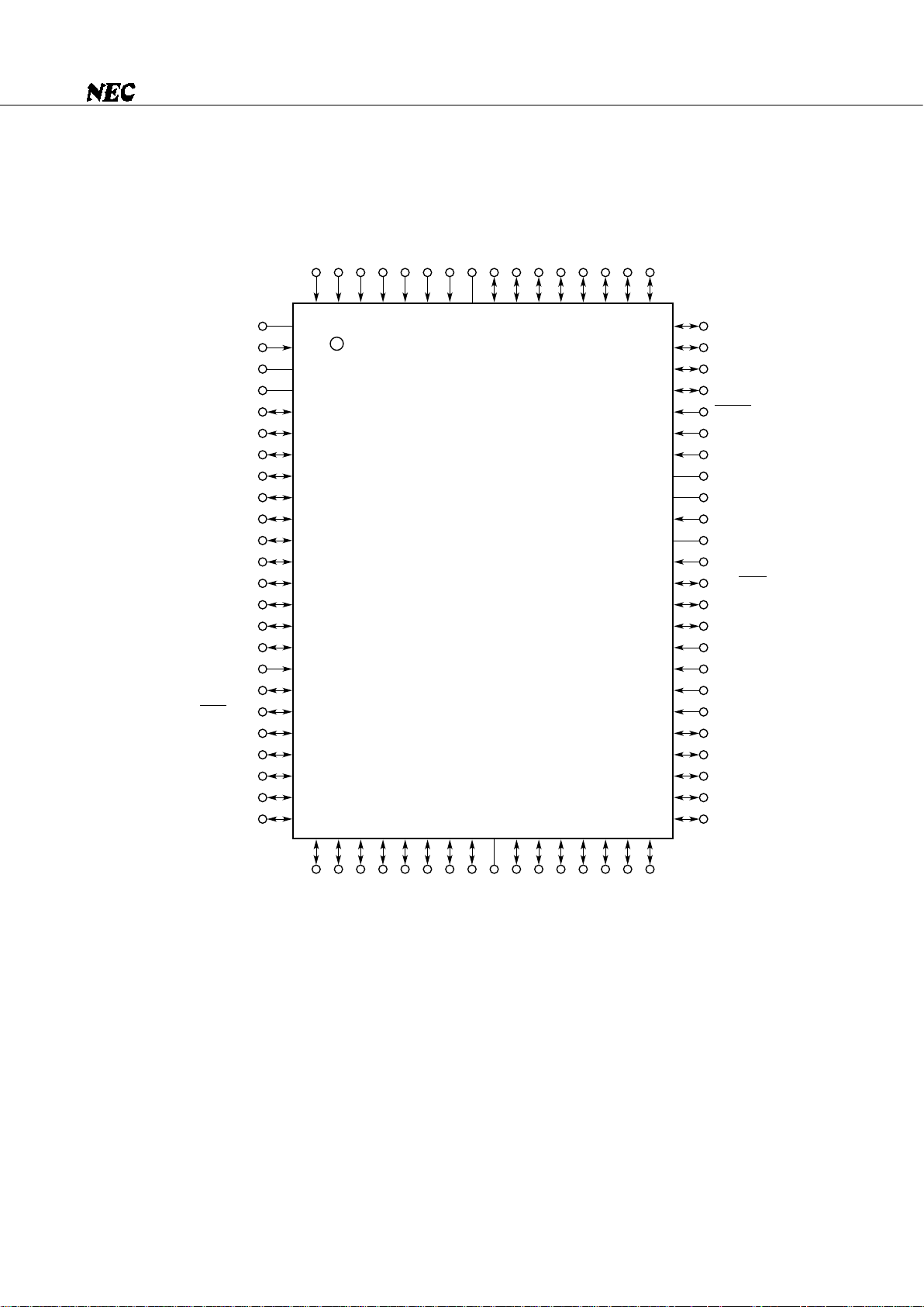
PIN CONFIGURATION (TOP VIEW)
IC: Internally connected. Connect the IC pin to VSS.
Note Be sure to supply power to both the VDD pins.
AN1
AN2
AN3
AN4/P150
AN5/P151
AN6/P152
AN7/P153
AV
SS
P120
P121
P122
P123
P130
P131
P132
P133
P140
P141
P142
P143
RESET
X2
X1
IC
XT2
XT1
V
SS
P00/INT4
P01/SCK0
P02/SO0/SB0
P03/SI0/SB1
P10/INT0
P11/INT1
P12/INT2
P13/TI0
P20/PTO0
P21
P22/PCL
P23/BUZ
P30
1
2
3
4
5
6
7
8
9
10
11
12
13
14
15
16
17
18
19
20
21
22
23
24
64
63
62
61
60
59
58
57
56
55
54
53
52
51
50
49
48
47
46
45
44
43
42
41
80 79 78 77 76 75 74 73 72 71 70 69 68 67 66 65
25 26 27 28 29 30 31 32 33 34 35 36 37 38 39 40
AN0
AV
REF
V
DD
V
DD
P113
P112
P111
P110
P103
P102
P101
P100
P93
P92
P91
P90
SI1/P83
SO1/P82
SCK1/P81
PPO/P80
KR7/P73
KR6/P72
KR5/P71
KR4/P70
KR3/P63
KR2/P62
KR1/P61
KR0/P60
P53
P52
P51
P50
V
SS
P43
P42
P41
P40
P33
P32
P31
Note
PD75517GF(A)-×××-3B9
µ
Page 4
4
µ
PD75517(A)
INTERNAL BLOCK DIAGRAM
TI0/P13
PTO0/P20
BUZ/P23
PPO/P80
SI0/SB1/P03
SO0/SB0/P02
SCK0/P01
SI1/P83
SO1/P82
SCK1/P81
INT0/P10
INT1/P11
INT2/P12
INT4/P00
KR0/P60
- KR7/P73
AN0 - AN3
AN4/P150
- AN7/P153
AV
REF
AVSS
P00 - P03
P10 - P13
P20 - P23
P30 - P33
P40 - P43
Note
P50 - P53
Note
P60 - P63
P70 - P73
P80 - P83
P90 - P93
P100 - P103
P110 - P113
P120 - P123
Note
P130 - P133
Note
P140 - P143
Note
P150 - P153
4
4
4
4
4
4
4
4
4
4
4
4
4
4
4
4
Port 0
Port 1
Port 2
Port 3
Port 4
Port 5
Port 6
Port 7
Port 8
Port 9
Port 10
Port 11
Port 12
Port 13
Port 14
Port 15
Basic
interval
timer
INTBT
Timer/event
counter #0
INTT0
Watch timer
INTW
Timer/pulse
generator
INTTPG
Serial bus
interface 0
INTCSI0
Serial
interface 1
Interrupt
control
Bit seq.
buffer (16)
A/D
converter
Program counter (15)
ROM program memory
24448 × 8 bits
ALU
CY
SP(8)
SBS(2)
Bank
Decode and
control
General register
RAM data memory
1024 × 4 bits
f
X/2
N
Clock output
control
PCL/P22
Clock divider
Clock generator
Sub Main
Stand by
control
XT1 XT2 X1 X2
CPU clock
Φ
RESET
VDD VSS
Note Port 4, Port 5, Port 12, Port 13, and Port 14 are N-ch open-drain
I/O ports with a medium withstand voltage of 10 V.
Page 5

5
µ
PD75517(A)
CONTENTS
1. PIN FUNCTIONS ........................................................................................................................ 7
1.1 PORT PINS ...................................................................................................................................... 7
1.2 NON-PORT PINS ............................................................................................................................ 9
1.3 PIN INPUT/OUTPUT CIRCUITS .................................................................................................... 10
1.4 CONNECTION OF UNUSED PINS ................................................................................................ 13
1.5 SELECTION OF A MASK OPTION ................................................................................................ 14
2. ARCHITECTURE AND MEMORY MAP OF THE µPD75517(A) .............................................. 15
2.1 DATA MEMORY BANK CONFIGURATION AND ADDRESSING MODES ................................ 15
2.2 GENERAL REGISTER BANK CONFIGURATION .......................................................................... 19
2.3 MEMORY-MAPPED I/O ................................................................................................................. 22
3. INTERNAL CPU FUNCTIONS.................................................................................................... 27
3.1 PROGRAM COUNTER (PC) ........................................................................................................... 27
3.2 PROGRAM MEMORY (ROM) ........................................................................................................ 27
3.3 DATA MEMORY (RAM) ................................................................................................................. 29
3.4 GENERAL REGISTERS ................................................................................................................... 31
3.5 ACCUMULATORS .......................................................................................................................... 32
3.6 STACK POINTER (SP) AND STACK BANK SELECT REGISTER (SBS) ..................................... 32
3.7 PROGRAM STATUS WORD (PSW) .............................................................................................. 35
3.8 BANK SELECT REGISTER (BS) ..................................................................................................... 38
4. PERIPHERAL HARDWARE FUNCTIONS .................................................................................. 39
4.1 DIGITAL I/O PORTS ....................................................................................................................... 39
4.2 CLOCK GENERATOR ...................................................................................................................... 51
4.3 CLOCK OUTPUT CIRCUIT ............................................................................................................. 60
4.4 BASIC INTERVAL TIMER ............................................................................................................... 63
4.5 CLOCK TIMER ................................................................................................................................. 67
4.6 TIMER/EVENT COUNTER ............................................................................................................. 69
4.7 TIMER/PULSE GENERATOR ......................................................................................................... 75
4.8 SERIAL INTERFACE (CHANNEL 0) ............................................................................................... 83
4.8.1 Serial Interface (Channel 0) Functions........................................................................ 84
4.8.2 Configuration of Serial Interface (Channel 0) ............................................................ 84
4.8.3 Register Functions ......................................................................................................... 86
4.8.4 Signals ............................................................................................................................. 94
4.8.5 Serial Interface (Channel 0) Operation ....................................................................... 100
4.8.6 Transfer Start in Each Mode ........................................................................................ 110
4.8.7 Manipulation of SCK0 Pin Output ............................................................................... 111
Page 6

6
µ
PD75517(A)
4.9 SERIAL INTERFACE (CHANNEL 1) ............................................................................................... 112
4.9.1 Serial Interface (Channel 1) Functions........................................................................ 112
4.9.2 Serial Interface (Channel 1) Configuration................................................................. 112
4.9.3 Register Functions ......................................................................................................... 114
4.9.4 Serial Interface (Channel 1) Operation ....................................................................... 115
4.10 A/D CONVERTER ........................................................................................................................... 117
4.11 BIT SEQUENTIAL BUFFER ............................................................................................................ 124
5. INTERRUPT FUNCTION ............................................................................................................ 125
5.1 CONFIGURATION OF THE INTERRUPT CONTROL CIRCUIT .................................................... 125
5.2 HARDWARE OF THE INTERRUPT CONTROL CIRCUIT .............................................................. 127
5.3 INTERRUPT SEQUENCE ................................................................................................................ 134
5.4 MULTIPLE INTERRUPT PROCESSING CONTROL ...................................................................... 135
5.5 VECTOR ADDRESS SHARE INTERRUPT PROCESSING ............................................................ 137
6. STANDBY FUNCTION ............................................................................................................... 138
6.1 SETTING OF STANDBY MODES AND OPERATION STATUSES ............................................. 138
6.2 RELEASE OF THE STANDBY MODES ......................................................................................... 139
6.3 OPERATION AFTER A STANDBY MODE IS RELEASED ............................................................ 141
7. RESET FUNCTION ..................................................................................................................... 142
8. INSTRUCTION SET .................................................................................................................... 144
8.1
µ
PD75517(A) INSTRUCTIONS ...................................................................................................... 144
8.2 INSTRUCTION SET AND ITS OPERATION .................................................................................. 147
8.3 INSTRUCTION CODES OF EACH INSTRUCTION ....................................................................... 156
9. ELECTRICAL CHARACTERISTICS............................................................................................. 162
10. PACKAGE DIMENSIONS ........................................................................................................... 174
11. RECOMMENDED SOLDERING CONDITIONS ......................................................................... 175
APPENDIX A SERIES PRODUCT FUNCTIONS ............................................................................ 176
APPENDIX B DEVELOPMENT TOOLS......................................................................................... 177
Page 7
7
µ
PD75517(A)
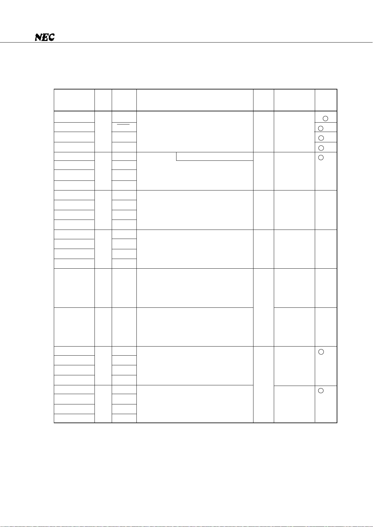
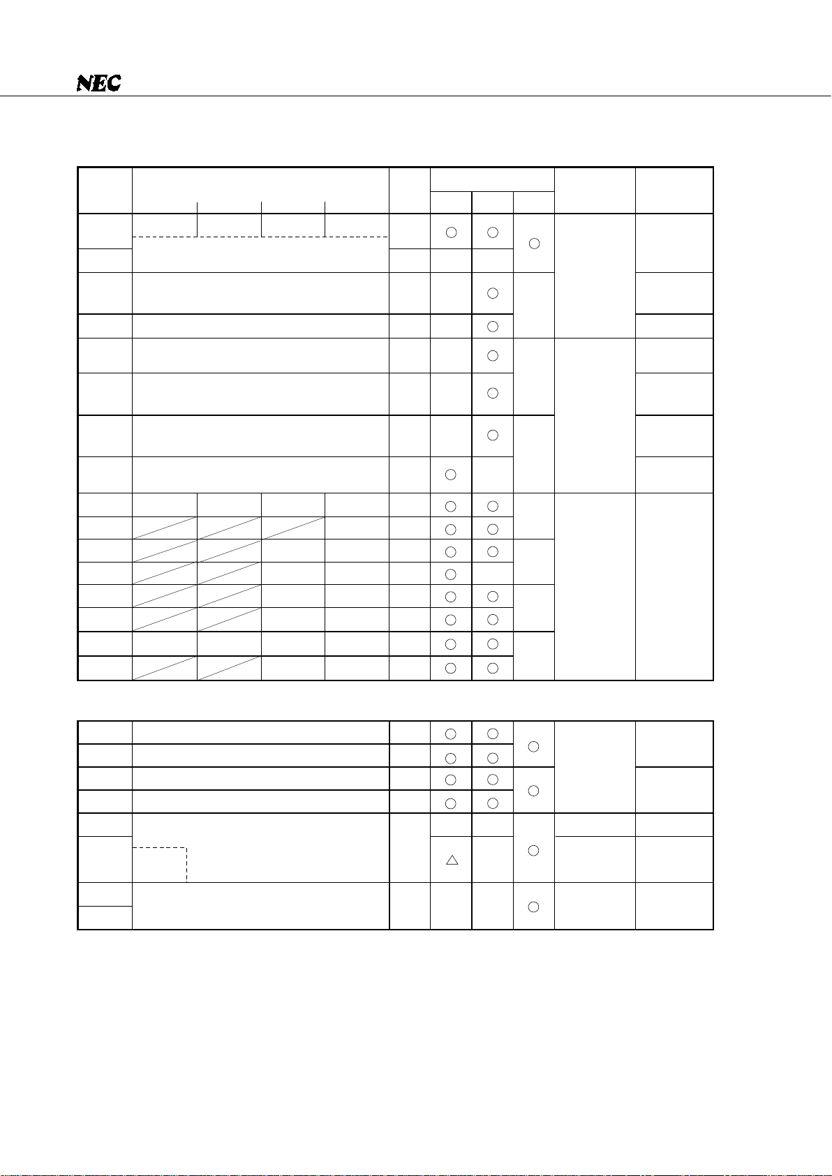
1. PIN FUNCTIONS
1.1 PORT PINS (1/2)
Notes 1. The circuits enclosed in circles have a Schmitt-triggered input.
2. An LED can be driven directly.
P00
P01
P02
P03
P10
P11
P12
P13
P20
P21
P22
P23
P30
Note 2
P31
Note 2
P32
Note 2
P33
Note 2
P40-P43
Note 2
P50-P53
Note 2
P60
P61
P62
P63
P70
P71
P72
P73
INT4
SCK0
SO0/SB0
SI0/SB1
INT0
INT1
INT2
TI0
PTO0
–
PCL
BUZ
–
–
–
–
–
–
KR0
KR1
KR2
KR3
KR4
KR5
KR6
KR7
×
×
×
×
❍
❍
With noise elimination function
4-bit input port (Port 0).
For P01 to P03, pull-up resistors can be
provided by software in units of 3 bits.
4-bit input port (Port 1).
Pull-up resistors can be provided by software
in units of 4 bits.
4-bit I/O port (Port 2).
Pull-up resistors can be provided by software
in units of 4 bits.
Programmable 4-bit I/O port (Port 3).
Input/output can be specified bit by bit.
Pull-up resistors can be provided by software
in units of 4 bits.
N-ch open-drain 4-bit I/O port (Port 4).
A pull-up resistor can be provided bit by bit
(mask option).
Withstand voltage is 10 V in open-drain mode.
N-ch open-drain 4-bit I/O port (Port 5).
A pull-up resistor can be provided bit by bit
(mask option).
Withstand voltage is 10 V in open-drain mode.
Programmable 4-bit I/O port (Port 6).
Input/output can be specified bit by bit.
Pull-up resistors can be provided by software
in units of 4 bits.
4-bit I/O port (Port 7).
Pull-up resistors can be provided by software
in units of 4 bits.
Also
used as
Pin name
I/O
B
F - A
F - B
M - C
B - C
E - B
E - C
M
M
F - C
F - A
8-bit I/O
Input
Input
Input
Input
High level
(when a pull-up
resistor is
provided) or
high impedance
High level
(when a pull-up
resistor is
provided) or
high impedance
Input
Input
When resetFunction
I
I
I/O
I/O
I/O
I/O
I/O
I/O
I/O
Note 1
circuit
type
Page 8
8
µ
PD75517(A)
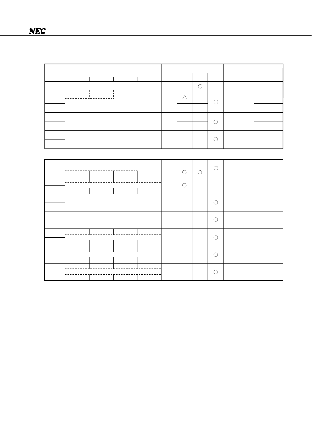
1.1 PORT PINS (2/2)
Note The circuits enclosed in circles have a Schmitt-triggered input.
×
×
×
×
×
×
×
Function
Also
used as
Pin name
I/O 8-bit I/O
When reset
I/O
Note
circuit
type
Input
Low level (when
a pull-down
resistor is
provided) or
high impedance
Input
Input
High level
(when a pull-up
resistor is
provided) or
high impedance
High level
(when a pull-up
resistor is
provided) or
high impedance
High level
(when a pull-up
resistor is
provided) or
high impedance
Input
PPO
SCK1
SO1
SI1
–
–
–
–
–
–
AN4-AN7
I
I/O
I/O
I/O
I/O
I/O
I/O
I
P80
P81
P82
P83
P90-P93
P100-P103
P110-P113
P120-P123
P130-P133
P140-P143
P150-P153
E
F
E
B
V
E
E
M
M
M
Y - A
4-bit input port (Port 8).
4-bit I/O port (Port 9).
A pull-down resistor can be provided bit by bit
(mask option).
4-bit I/O port (Port 10)
4-bit I/O port (Port 11)
N-ch open-drain, 4-bit I/O port (Port 12).
Pull-up resistors can be provided bit by bit
(mask option).
Withstand voltage is 10 V in open-drain mode.
N-ch open-drain, 4-bit I/O port (Port 13).
Pull-up resistors can be provided bit by bit
(mask option).
Withstand voltage is 10 V in open-drain mode.
N-ch open-drain, 4-bit I/O port (Port 14).
Pull-up resistors can be provided bit by bit
(mask option).
Withstand voltage is 10 V in open-drain mode.
4-bit input port (Port 15)
Page 9
9
µ
PD75517(A)
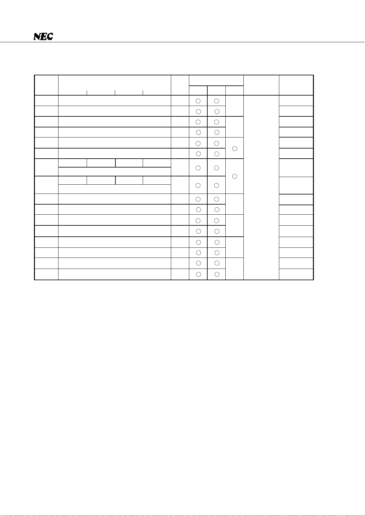
1.2 NON-PORT PINS
Notes 1. The circuits enclosed in circles have a Schmitt-triggered input.
2. Be sure to input V
SS level to this pin.
Function
Also
used as
Pin name
I/O
I
O
O
O
I/O
I/O
I/O
I
I
I
I
I
I/O
O
I
I
I
–
I
I
–
I
O
–
–
–
Synchronous
Asynchronous
Asynchronous
Edge detection vectored interrupt input pin
(The edge to be detected is selectable.)
Edge detection testable input pin
(An rising edge is detected.)
P13
P20
P22
P23
P01
P02
P03
P00
P10
P11
P12
P60-P63
P70-P73
P81
P82
P83
–
P150-P153
–
–
–
–
–
P80
–
–
–
External event pulse input pin for the timer/event counter
Timer/event counter output pin
Clock output pin
Fixed frequency output pin (for buzzer or system clock
trimming)
Serial clock I/O pin
Serial data output pin or serial bus I/O pin
Serial data input pin or serial bus I/O pin
Edge detection vectored interrupt input pin (Either a rising
or falling edge is detected.)
Parallel-falling-edge-sensitive testable input pins
Parallel-falling-edge-sensitive testable input pins
Serial clock I/O pin
Serial data output pin
Serial data input pin
Analog input pins to A/D converter
A/D converter reference voltage input pin
A/D converter reference GND pin
Pin for connection to a crystal/ceramic resonator for main
system clock generation. When external clock is used, it is
input to X1, and its inverted signal is input to X2.
Pin for connection to a crystal resonator for subsystem
clock generation. When external clock is used, it is input to
XT1, and XT2 is left open.
System reset input pin
Timer/pulse generator pulse output pin
Positive power supply pin
Ground pin
Internally connected
Note 2
–
Input
Input
Input
Input
Input
Input
–
–
–
Input
Input
Input
Input
Input
–
–
–
–
–
–
Input
–
–
–
TI0
PTO0
PCL
BUZ
SCK0
SO0/SB0
SI0/SB1
INT4
INT0
INT1
INT2
KR0-KR3
KR4-KR7
SCK1
SO1
SI1
AN0-AN3
AN4-AN7
AVREF
AVSS
X1, X2
XT1
XT2
RESET
PPO
VDD
VSS
IC
I/O
Note 1
circuit
type
When reset
B - C
E - B
E - B
E - B
F - A
F - B
M - C
B
B - C
B - C
F - C
F - A
F
E
B
Y
Y - A
Z
–
–
–
B
E
–
–
–
Page 10
10
µ
PD75517(A)
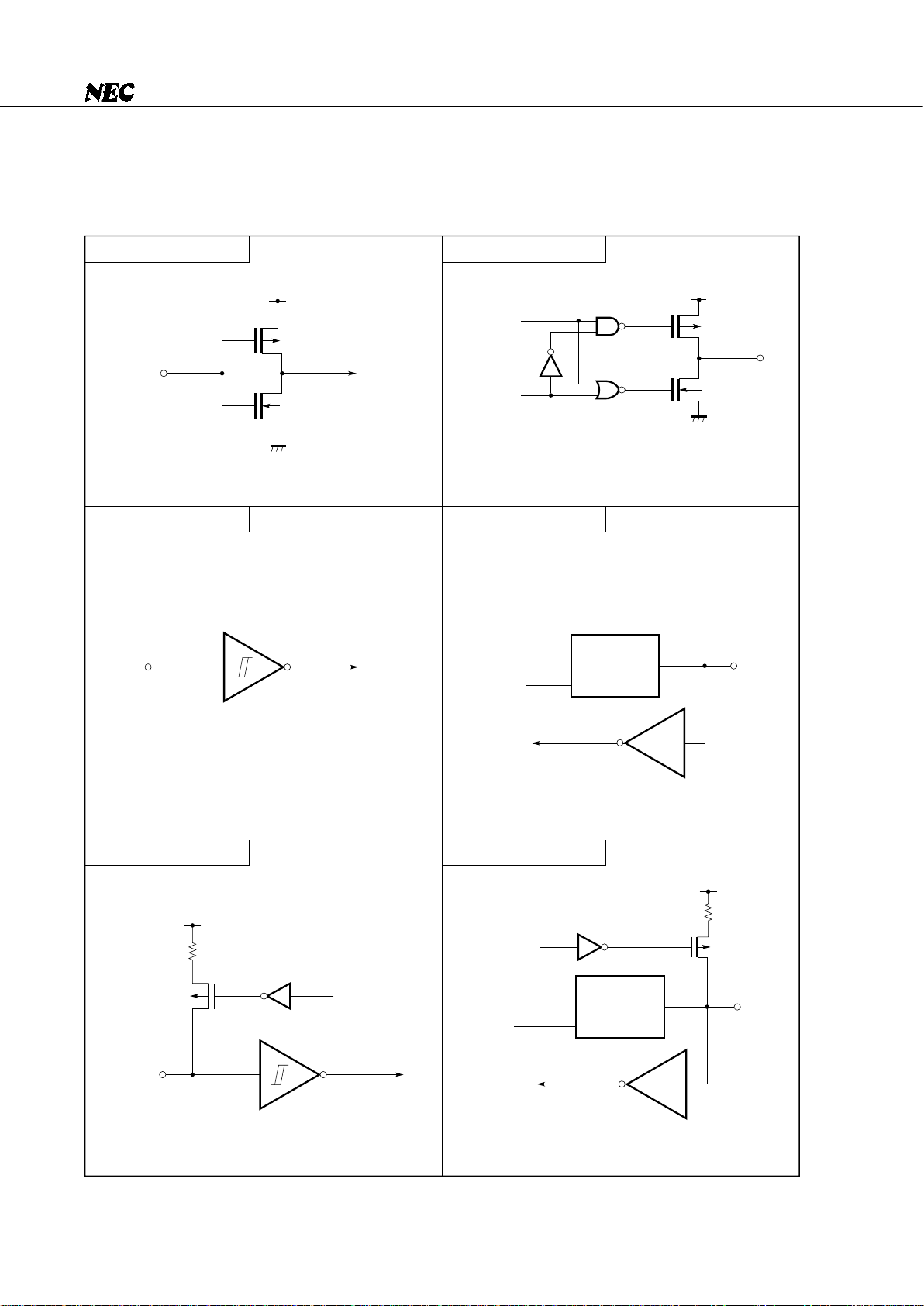
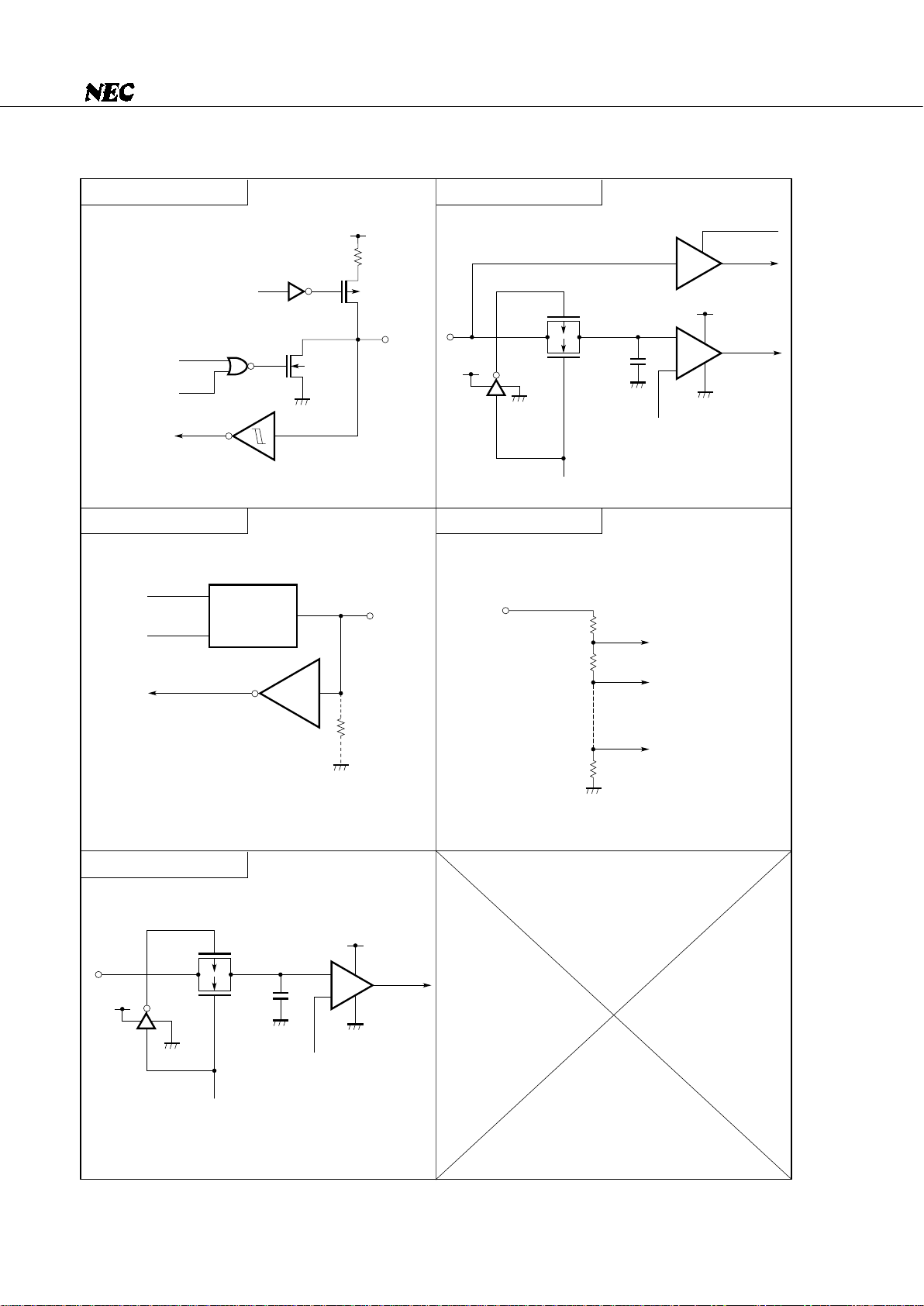
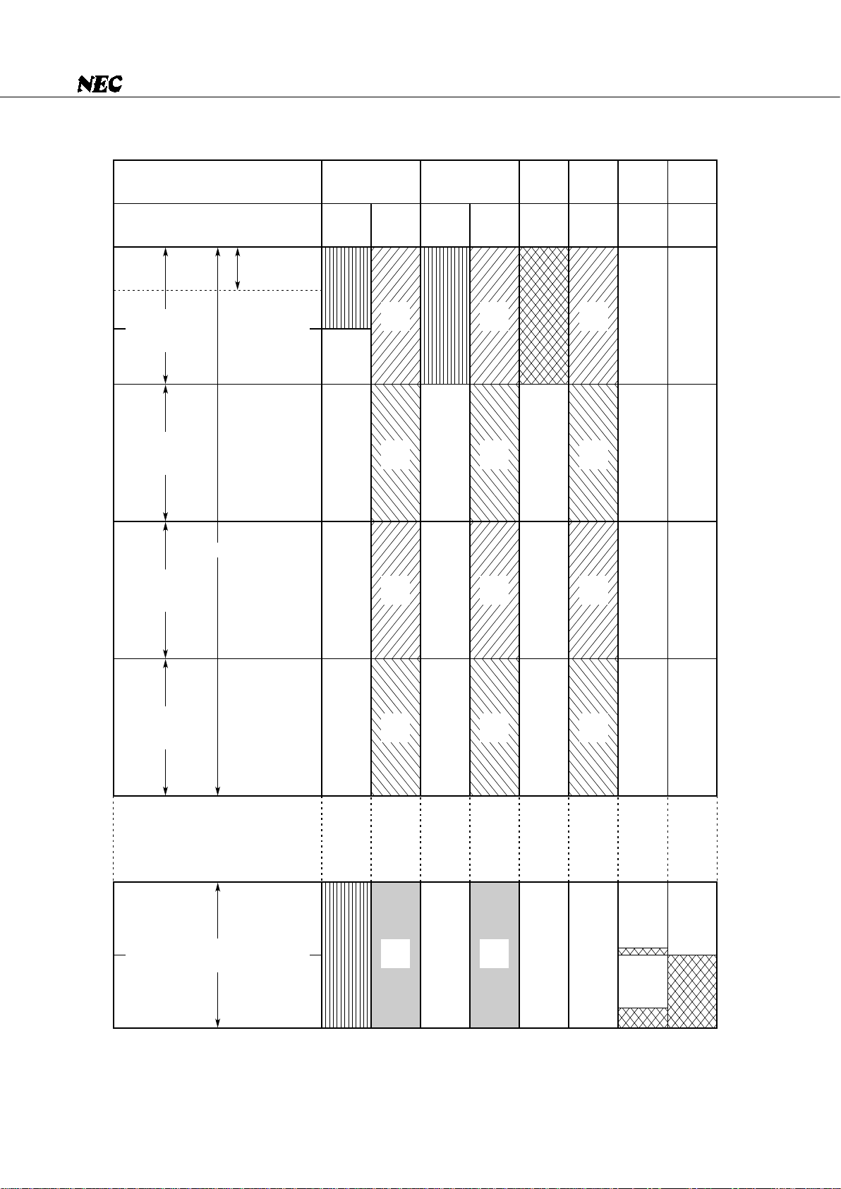
1.3 PIN INPUT/OUTPUT CIRCUITS
Fig. 1-1 shows the input/output circuit of each
µ
PD75517(A) pin in a simplified manner.
Fig. 1-1 Pin Input/Output Circuits (1/3)
Type A
CMOS input buffer
Schmitt trigger input with hysteresis
Push-pull output which can be set to high-impedance output
(off for both P-ch and N-ch)
I/O circuit consisting of a push-pull output
of type D and an input buffer of type A
P.U.R.: Pull-Up Resistor
Type B Type E
Type B - C
Type D
VDD
IN
P-ch
N-ch
IN
IN
P-ch
P.U.R.
enable
P.U.R.
V
DD
VDD
P-ch
N-ch
OUT
Data
Output
disable
IN/OUT
Data
Output
disable
Type D
Schmitt trigger input with hysteresis
P.U.R.: Pull-Up Resistor
P.U.R.
V
DD
Output
disable
P-ch
IN/OUT
Data
Output
disable
Type D
Type E - B
Type A
Type A
Page 11
11
µ
PD75517(A)
Fig. 1-1 Pin Input/Output Circuits (2/3)
Type E - C
I/O circuit consisting of a push-pull output of type D
and a Schmitt-triggered input of type B
P.U.R.: Pull-Up Resistor
Type F
Type F - A
Type F - B
P.U.R.
V
DD
P.U.R.
enable
P-ch
IN/OUT
Data
Output
disable
Type D
IN/OUT
Data
Output
disable
Type D
P.U.R.: Pull-Up Resistor
P.U.R.
V
DD
P.U.R.
enable
P-ch
IN/OUT
Data
Output
disable
Type D
P.U.R.: Pull-Up Resistor
VDD
P-ch
N-ch
IN/OUT
VDD
P-ch
P.U.R.
P.U.R.
enable
Output
disable
(P-ch)
Data
Output
disable
Output
disable
(N-ch)
Type F - C
P.U.R.: Pull-Up Resistor
P.U.R.
V
DD
P.U.R.
enable
P-ch
IN/OUT
Data
Output
disable
Type D
Type M
P.U.R.: Pull-Up Resistor
N-ch
(Can sustain
+9 V)
IN/OUT
Data
VDD
Output
disable
P.U.R.
(Mask option)
Middle-voltage input buffer
(Can sustain + 10 V)
Type B
Type A
Type B
Type B
Type B
Page 12
12
µ
PD75517(A)
Fig. 1-1 Pin Input/Output Circuits (3/3)
Type V
Type M - C
Type Y
Type Z
Type Y - A
P.D.R.: Pull-Down Resistor
P.U.R.: Pull-Up Resistor
P.D.R.
(Mask option)
IN/OUT
Data
Output
disable
Type D
N-ch
P.U.R.
Data
Output
disable
P.U.R.
enable
V
DD
P-ch
IN/OUT
V
DD
V
DD
P-ch
AV
SS
N-ch
Sampl-
ing C
AV
SS
Reference voltage
(from voltage tap of
serial resistor string)
Input
enable
IN
V
DD
AV
SS
Sampl-
ing C
V
DD
AV
SS
IN
P-ch
N-ch
Reference voltage
(from voltage tap of
serial resistor string)
IN instruction
+
–
Input
enable
AV
REF
Reference voltage
AV
SS
+
–
Type A
Page 13
13
µ
PD75517(A)
1.4 CONNECTION OF UNUSED PINS
Table 1-1 Recommended Connection of Unused Pins
To be connected to VSS
To be connected to VSS or VDD
To be connected to VSS
Input state : To be connected to VSS or VDD
Output state : To be left open
To be connected to VSS or VDD
Input state : To be connected to VSS or VDD
Output state : To be left open
To be connected to VSS
To be connected to VSS or VDD
To be left open
To be connected to VSS
P00/INT4
P01/SCK0
P02/SO0/SB0
P03/SI1/SB1
P10/INT0-P12/INT2
P13/TI0
P20/PTO0
P21
P22/PCL
P23/BUZ
P30-P33
P40-P43
P50-P53
P60/KR0-P63/KR3
P70/KR4-P73/KR7
P80/PPO
P81/SCK1
P82/SO1
P83/SI1
P90-P93
P100-P103
P110-P113
P120-P123
P130-P133
P140-P143
P150/AN4-P153/AN7
AN0-AN3
XT1
XT2
AVREF
AVSS
IC
Pin name Recommended connection
Page 14
14
µ
PD75517(A)
1.5 SELECTION OF A MASK OPTION
The following mask options are provided for pins.
(1) Specification of built-in pull-up and pull-down resistors
Table 1-2 Selection of Pull-Up and Pull-Down Resistors
(2) Specification of built-in feed-back resistors for subsystem clock oscillation
Table 1-3 Selection of Feed-Back Resistors
Caution Even if built-in feed-back resistors are provided when no subsystem clock is used, operation is
not affected except increased power supply current I
DD.
P40-P43,
P50-P53,
P120-P123,
P130-P133,
P140-P143
P90-P93
Pin name
2 No pull-up resistor provided
(Can be specified bit by bit.)
2 No pull-down resistor provided
(Can be specified bit by bit.)
1 Pull-up resistors provided
(Can be specified bit by bit.)
1 Pull-down resistors provided
(Can be specified bit by bit.)
Mask option
XT1, XT2 1 Feed-back resistors provided
(when a subsystem clock is used)
2 No feed-back resistors provided
(when no subsystem clock is used)
Mask optionPin name
Page 15
15
µ
PD75517(A)
2. ARCHITECTURE AND MEMORY MAP OF THE µPD75517(A)
The µPD75517(A) has three architectural features:
(a) Data memory bank configuration
(b) General register bank configuration
(c) Memory-mapped I/O
Each of these features is explained below.
2.1 DATA MEMORY BANK CONFIGURATION AND ADDRESSING MODES
As shown in Fig. 2-1, the data memory space of the
µ
PD75517(A) contains a static RAM (1024 words × 4
bits) at addresses 000H to 3FFH and peripheral hardware (such as I/O ports and timers) at addresses F80H to
FFFH. To address a 12-bit address in this data memory space, the µPD75517(A) uses such a memory bank
configuration that the low-order eight bits are specified with an instruction directly or indirectly, and the highorder four bits are used to specify a memory bank (MB).
To specify a memory bank (MB), a memory bank enable flag (MBE) and memory bank select register (MBS)
are contained, allowing the addressing indicated in Fig. 2-1 and 2-2 and Table 2-1. (The MBS is a register used
to select a memory bank, and can be set to 0, 1, 2, 3, or 15. The MBE is a flag used to determine whether a
memory bank selected using the MBS register is to be enabled. The MBE is automatically saved or restored
at the time of interrupt processing or subroutine processing, so that it can be freely set in interrupt processing
and subroutine processing.)
In addressing data memory space, the MBE is usually set to 1 (MBE = 1), and the static RAM in the memory
bank specified by the MBS is operated. However, the MBE = 0 mode or the MBE = 1 mode can be selected
for each step of program processing for more efficient programming.
The MBE and MBS are set as indicated below.
Example SET1 MBE ; MBE ← 1
CLR1 MBE ; MBE ← 0
SEL MB0 ; MBS ← 0
SEL MB1 ; MBS ← 1
SEL MB15 ; MBS ← 15
• Interrupt processing
• Processing that repeats internal hardware and static RAM operations
• Subroutine processing
• Usual program processing
MBE = 0 mode
MBE = 1 mode
Applicable program processing
Page 16
16
µ
PD75517(A)
Fig. 2-1 Data Memory Organization and Addressing Range of Each Addressing Mode
Remark — : Don’t care
FF0H
FFFH
FB0H
FBFH
FC0H
F80H
3FFH
2FFH
300H
1FFH
200H
0FFH
100H
01FH
020H
07FH
000H
Addressing mode
mem
mem.bit
@HL
@H + mem.bit
@DE
@DL
Stack
address-
ing
fmem.bit
pmem.
@L
Memory bank enable flag
MBE
= 0
MBE
= 1
MBE
= 0
MBE
= 1
––– –
Data area
Static RAM
(memory bank 0)
Data area
Static RAM
(memory bank 1)
Data area
Static RAM
(memory bank 2)
Data area
Static RAM
(memory bank 3)
Stack area
Not contained
Peripheral hardware area
(memory bank 15)
MBS
= 0
MBS
= 0
SBS
= 0
MBS
= 1
MBS
= 1
SBS
= 1
MBS
= 2
MBS
= 2
SBS
= 2
MBS
= 3
MBS
= 3
SBS
= 3
MBS
= 15
MBS
= 15
General
resister
area
Page 17
17
µ
PD75517(A)
Table 2-1 Addressing Modes
Bit specified by bit at the address specified by MB and mem. In this case:
When MBE = 0 and mem = 00H-7FH, MB = 0
When MBE = 0 and mem = 80H-FFH, MB = 15
When MBE = 1, MB = MBS
Address specified by MB and mem. In this case:
When MBE = 0 and mem = 00H-7FH, MB = 0
When MBE = 0 and mem = 80H-FFH, MB = 15
When MBE = 1, MB = MBS
Address specified by MB and mem (mem: even address). In this case:
When MBE = 0 and mem = 00H-7FH, MB = 0
When MBE = 0 and mem = 80H-FFH, MB = 15
When MBE = 1, MB = MBS
Address specified by MB and HL.
In this case, MB = MBE•MBS
Address specified by DE in memory bank 0
Address specified by DL in memory bank 0
Address specified by MB and HL (with the L register holding an even number).
In this case, MB = MBE•MBS
Bit specified by bit at the address specified by fmem. In this case:
fmem = FB0H-FBFH (interrupt-related hardware)
fmem = FF0H-FFFH (I/O port)
Bit specified by the low-order 2 bits of the L register at the address specified
by the high-order 10 bits of pmem and the high-order 2 bits of the L register.
In this case, pmem = FC0H-FFFH
Bit specified by bit at the address specified by MB, H, and the low-order 4 bits
of mem.
In this case, MB = MBE•MBS
Address specified by SP in memory bank 0, 1, 2, and 3 selected by SBS
1-bit direct addressing
4-bit direct addressing
8-bit direct addressing
4-bit register indirect
addressing
8-bit register indirect
addressing
Bit manipulation
addressing
Stack addressing
mem.bit
mem
@HL
@HL+
@HL–
@DE
@DL
@HL
fmem.bit
pmem.@L
@H+mem.bit
—
Representation
format
Specified addressAddressing mode
Page 18
18
µ
PD75517(A)
As summarized in Table 2-1, the µPD75517(A) allows both direct and indirect addressing in data memory
manipulation for 1-bit data, 4-bit data, and 8-bit data, so that very efficient and simple programming can be
performed.
Examples 1. The 8-bit data of port 4 and port 5 are transferred to addresses 20H and 21H.
CLR1 MBE ; MBE ← 0
IN XA, PORT4 ; XA ← Ports 5, 4
MOV 20H, XA ; (21H, 20H) ← XA
2. When P02 is 0, P33 is set.
SKT PORT0.2 ; Skip if bit 2 of port 0 is 1
SET1 PORT3.3 ; Set bit 3 of port 3
3. A different value is output to port 6, depending on the status of P10.
SKF PORT1.0 ; Skip if bit 0 of port 1 is 0
MOV A, #1010B ; A ← 1010B (string effect)
MOV A, #0101B ; A ← 0101B (string effect)
SEL MB15 ; or CLR1 MBE
OUT PORT6, A ; Port 6 ← A
Fig. 2-2 Updating Static RAM Addresses
INCS D
DECS D
INCS LDECS L
INCS D
DECS D
INCS EDECS E
INCS H
DECS H
INCS LDECS L
INCS H
DECS H
× 0H
0 × H
F × H
@DL
4-bit transfer
@DE
4-bit transfer
@HL
4-bit
manipulation
8-bit
manipulation
@H + mem.bit
Bit manipulation
Direct
addressing
Bit manipulation
4-bit
8-bit
× FH
DECS DE INCS DE
DECS HL INCS HL
Automatic
decrement
Automatic
increment
Page 19
19
µ
PD75517(A)
2.2 GENERAL REGISTER BANK CONFIGURATION
The
µ
PD75517(A) contains four register banks, each consisting of eight general registers: X, A, B, C, D, E,
H, and L. These registers are mapped to addresses 00H to 1FH in memory bank 0 of the data memory. (See
Fig. 2-3.) To specify a general register bank, a register bank enable flag (RBE) and a register bank select register
(RBS) are contained. The RBS is a register used to select a register bank, and the RBE is a flag used to determine
whether a register bank selected using the RBS is to be enabled. The register bank (RB) enabled at instruction
execution is determined as RB = RBE•RBS
As indicated in Table 2-2, the
µ
PD75517(A) enables the user to create programs in a very efficient manner
by selecting a register bank from the four register banks, depending on whether the processing is normal
processing or interrupt processing. (The RBE is automatically saved and set at the time of interrupt processing,
and is automatically restored upon completion of interrupt processing.)
Table 2-2 Example of the Use of Register Banks with Normal Routines and Interrupt Routines
The RBE and RBS are set as indicated below.
Example SET1 RBE ; RBE ← 1
CLR1 RBE ; RBE ← 0
SEL RB0 ; RBS ← 0
SEL RB3 ; RBS ← 3
The general registers allow transfers, comparisons, arithmetic/logical operations, and increments and
decrements not only on a 4-bit basis, but also on an 8-bit basis with the XA, HL, DE, and BC register pairs.
In this case, the register pairs of the register bank that has the inverted value of bit 0 of a register bank specified
by RBE•RBS can be specified as XA’, HL’, DE’, and BC’, thus providing eight 8-bit registers. (See Fig. 2-4.)
Example SET1 RBE ; RBE ← 1
SEL RB2 ; RBS ← 2
MOV XA, #18H ; XA ← 18H
ADDS HL, XA ; HL ← HL+XA
SUBS HL’, XA ; HL’ ← HL’–XA (HL’ is HL of register bank 3)
INCS HL ; HL ← HL+1
MOV XA, #00H ; XA ← 00H (string effect)
MOV XA, #10H ; XA ← 10H (string effect)
Normal processing
Single interrupt processing
Dual interrupt processing
Multiple (triple or more) interrupt processing
Use register banks 2 and 3 with RBE = 1.
Use register bank 0 with RBE = 0.
Use register bank 1 with RBE = 1.
(In this case, the RBS needs to be saved and restored.)
Save the registers with PUSH or POP.
Page 20
20
µ
PD75517(A)
Fig. 2-3 General Register Configuration (4-Bit Processing)
X
H
D
B
X
H
D
B
X
H
D
B
X
H
D
B
01H
03H
05H
07H
09H
0BH
0DH
0FH
11H
13H
15H
17H
19H
1BH
1DH
1FH
A
L
E
C
A
L
E
C
A
L
E
C
A
L
E
C
00H
02H
04H
06H
08H
0AH
0CH
0EH
10H
12H
14H
16H
18H
1AH
1CH
1EH
Register bank 0
(RBE·RBS = 0)
Register bank 1
(RBE·RBS = 1)
Register bank 2
(RBE·RBS = 2)
Register bank 3
(RBE·RBS = 3)
Page 21
21
µ
PD75517(A)
Fig. 2-4 General Register Configuration (8-Bit Processing)
XA
HL
DE
BC
XA’
HL’
DE’
BC’
00H
02H
04H
06H
08H
0AH
0CH
0EH
When RBE·RBS
= 0
XA’
HL’
DE’
BC’
XA
HL
DE
BC
00H
02H
04H
06H
08H
0AH
0CH
0EH
When RBE·RBS
= 1
XA
HL
DE
BC
XA’
HL’
DE’
BC’
10H
12H
14H
16H
18H
1AH
1CH
1EH
When RBE·RBS
= 2
XA’
HL’
DE’
BC’
XA
HL
DE
BC
10H
12H
14H
16H
18H
1AH
1CH
1EH
When RBE·RBS
= 3
Page 22
22
µ
PD75517(A)
2.3 MEMORY-MAPPED I/O
The
µ
PD75517(A) employs memory-mapped I/O, which maps peripheral hardware such as timers and I/O
ports to addresses F80H to FFFH in the data memory space as shown in Fig. 2-1. This means that there is no
particular instruction to control peripheral hardware, but all peripheral hardware is controlled using memory
manipulation instructions. (Some mnemonics for hardware control are available to make programs readable.)
To manipulate peripheral hardware, the addressing modes listed in Table 2-3 can be used.
Table 2-3 Addressing Modes Applicable to Peripheral Hardware
Fig. 2-5 summarizes the I/O map of the
µ
PD75517(A).
The items in Fig. 2-5 have the following meanings:
• Symbol: Name representing the address of incorporated hardware, which can be coded in the operand
field of an instruction
• R/W : Indicates whether the hardware allows read/write operation.
R/W: Both read and write operations possible
R : Read only
W : Write only
• Number of manipulatable bits:
Indicates the number of bits that can be processed in hardware manipulation
: Bits can be manipulated on an indicated bit (1-, 4-, or 8-bit) basis.
: Particular bits can be manipulated. For these bits, see Remarks.
: Bits cannot be manipulated on an indicated bit (1-, 4-, or 8-bit) basis.
• Bit manipulation addressing:
Bit manipulation addressing applicable in hardware bit manipulation
Bit manipulation
4-bit manipulation
8-bit manipulation
Direct addressing mode specifying mem.bit with MBE = 0 or
(MBE = 1, MBS = 15)
Direct addressing mode specifying fmem.bit regardless of MBE
and MBS setting
Indirect addressing mode specifying pmem.@L regardless of
MBE and MBS setting
Direct addressing mode specifying mem with MBE = 0 or (MBE
= 1, MBS = 15)
Register indirect addressing mode specifying @HL with (MBE
= 1, MBS = 15)
Direct addressing mode specifying mem (even address) with
MBE = 0 or (MBE = 1, MBS = 15)
Register indirect addressing mode specifying @HL (with the L
register containing an even number) with (MBE = 1, MBS = 15)
All hardware allowing bit
manipulation
IST0, IST1, MBE, RBE, EOT,
IE×××, IRQ×××, PORTn.×
BSBn.×
PORTn.×
All hardware allowing 4-bit
manipulation
All hardware allowing 8-bit
manipulation addressing
Applicable addressing mode
Applicable hardware
–
Page 23
23
µ
PD75517(A)
Fig. 2-5 µPD75517(A) I/O Map (1/4)
Notes 1. Can be operated separately as the RBS and MBS during 4-bit manipulation.
Can also be operated as the BS during 8-bit manipulation.
2. TOE0: Timer/event counter 0 output enable flag (W)
R/W – –
W
–
R/W
Address
b0b1b2b3
F80H
F85H
F86H
F98H
FA0H
FA2H
FA4H
FA6H
TOE0
Note 2
R
W
W
W
R
W
––
–
––
–
––
––
––
––
–
mem.bit
mem.bit
mem.bit
Remarks
Bit
manipulation
addressing
Bit 0 is fixed
to 0
Hardware name (symbol)
Number of bits that
Stack pointer (SP)
Basic interval timer mode register (BTM)
Basic interval timer (BT)
Clock mode register (WM)
Timer/event counter 0 mode register (TM0)
Timer/event counter 0 count register (T0)
Timer/event counter 0 modulo register (TMOD0)
Only bit 3
allows bit
manipulation.
Only bit 3 can
be manipulat-
ed
1 bit 4 bits 8 bits
F82H
F83H
F84H
Register bank select register
(RBS)
Memory bank select register
(MBS)
Bank select
register (BS)
Stack bank select register (SBS) R/W
Bits 3 and 2
are always
set to 0.
R
Note 1
–
–
––
F90H
F94H
Timer pulse generator (TPGM)
mem.bit
Only bit 3 can
be manipulat-
ed
–
W
––
F96H
Timer/pulse generator modulo register (MODL)
R/W
––
Timer/pulse generator modulo register (MODH) R/W
––
–
can be manipulated
Page 24
24
µ
PD75517(A)
Fig. 2-5 µPD75517(A) I/O Map (2/4)
Remarks 1. IE××× : Interrupt enable flag
2. IRQ×××: Interrupt request flag
R/W
–
R/WAddress
b0b1b2b3
FB0H
FB2H
FB3H
FC0H
FC2H
FC3H
fmem.bit
mem.bit
pmem.@L
RBEMBEIST0IST1
––
R
–
–
–
–
–
–
W
W
W
W
W
–
–
R/W
–
R/W
R/W
R/W
–
R/W
–
R/W
fmem.bit
FB4H
FB5H
FB6H
FB7H
FB8H
FBAH
FBCH
FBDH
FBEH
FBFH
IE4 IRQ4 IEBT IRQBT
IEW IRQW
IET0 IRQT0
IECSI0 IRQCSI0
IE0 IRQ0
IE2 IRQ2
IE1 IRQ1
R/W
R/W
R/W
R/W
FC1H
Remarks
Bit
manipulation
addressing
Hardware name (symbol)
1 bit 4 bits 8 bits
Program status word (PSW)
Processor clock control register (PCC)
INT0 mode register (IM0)
INT1 mode resistor (IM1)
INT2 mode register (IM2)
System clock control register (SCC)
Bit sequential buffer 0 (BSB0)
Bit sequential buffer 1 (BSB1)
Bit sequential buffer 2 (BSB2)
Bit sequential buffer 3 (BSB3)
Manipulated
with EI/DI
instruction
Bit 2 is fixed
to 0
Bits 3, 2, and
1 are fixed to
0
Bits 3 and 2
are fixed to
0
Bits 2 and 1
are fixed to 0
–
Interrupt priority select register (IPS)
W
FBBH
IETPG IRQTPG
FB9H
EOT R/W
R/W
–
FC8H
Serial operation mode register 1 (CSIM1)
Only bit 7
allows bit
manipulation.
FCCH
Serial I/O shift register 1 (SIO1)
CSIE1
W
R/W
––
–
––
mem.bit
Number of bits that
can be manipulated
Page 25
25
µ
PD75517(A)
Fig. 2-5 µPD75517(A) I/O Map (3/4)
Note When developing a program, set 0 to the following two bits of the port mode register group C (PMGC):
FEEH, b0 (Equivalent to PM8)
FEFH, b3 (Equivalent to PM15)
For, while this port on the chip side is used for input only, the corresponding port on the emulator
is an I/O port.
W
R/WAddress
b0b1b2b3
FD0H
FD8H
FDAH
–
–
––
W
–
–
R
W
FDCH
EOCSOC
–
–
–
b3: 1-bit write
b2: 1-bit read
W
R/W
FE0H
FE2H
FE4H
mem.bit
–
–
–
W
FE6H
–
–
R/W
––
mem.bit
FE8H
FEEH
–
W
–
–
W
–
PM32PM33 PM31 PM30
PM10
PM11
PM9 –
Note
PM62PM63 PM61 PM60
PM14
PM13 PM12
R/W
Remarks
Bit
manipulation
addressing
Hardware name (symbol)
1 bit 4 bits 8 bits
Clock output mode register (CLOM)
A/D conversion mode register (ADM)
SA register (SA)
Pull-up resistor specification register group A
(POGA)
Serial operation mode register 0 (CSIM0)
SBI control register (SBIC)
Serial I/O shift register 0 (SIO0)
Slave address register (SVA)
Port mode register group A (PMGA)
Port mode register group C (PMGC)
b6: 1-bit read
All bits allow
bit manipula-
tion only
–
––
COICSIE0 WUP
RELDCMDD CMDT RELT
ACKDBSYE
ACKE ACKT
FECH
–
W
–
PM2
–
––
–PM7
PM5 PM4
Port mode register group B (PMGB)
–
Note
Number of bits that
can be manipulated
Page 26
26
µ
PD75517(A)
Fig. 2-5 µPD75517(A) I/O Map (4/4)
Note KR0 to KR7 are read-only. In 4-bit parallel input processing, PORT6 or PORT7 is specified.
R
R/WAddress
b0b1b2b3
FF0H
FF1H
FF3H
fmem.bit
pmem.@L
FF5H
R
–
KR2KR3 KR1 KR0
FF2H
FF4H
FF6H
Note
FFBH
R/W
R/W
R/W
R/W
R/W
R
–
–
Remerks
Bit
manipulation
addressing
Hardware name (symbol)
1 bit 4 bits 8 bits
Port 0 (PORT0)
Port 1 (PORT1)
Port 3 (PORT3)
Port 5 (PORT5)
Port 2 (PORT2)
Port 4 (PORT4)
Port 11 (PORT11)
Port 6 (PORT6)
KR6KR7 KR5 KR4
FF7H
Note
R/W
Port 7 (PORT7)
R/W
R/W
R/W
Port 9 (PORT9)
Port 8 (PORT8)
Port 10 (PORT10)
Port 15 (PORT15)
Port 13 (PORT13)
Port 12 (PORT12)
Port 14 (PORT14)
R
R/W
R/W
R/W
–
–
–
FFAH
FF9H
FF8H
FFCH
FFDH
FFEH
FFFH
Number of bits that
can be manipulated
Page 27

27
µ
PD75517(A)
3. INTERNAL CPU FUNCTIONS
3.1 PROGRAM COUNTER (PC): 15 BITS
The program counter is a 15-bit binary counter for holding program memory address information.
Fig. 3-1 Program Counter Format
Note that the reset start address must be set within a space of 16K bytes (0000H to 3FFFH). This is because
a RESET input sets the low-order six bits of program memory address 0000H in PC13 to PC8, and the contents
of address 0001H in PC7 to PC0, and 0 in PC14 for initialization.
3.2 PROGRAM MEMORY (ROM): 24448 WORDS × 8 BITS
The program memory is a mask-programmable ROM with a configuration of 24448 words × 8 bits for storing
programs, table data, and so forth.
Program memory is addressed by the program counter. Table data can be referenced using the table
reference instruction (MOVT).
Fig. 3-2 shows the allowable branch address ranges for the branch instructions and subroutine call
instructions. The whole-space branch instruction (BRA !addr1) and the whole-space call instruction (CALLA
!addr1) allow a direct branch throughout the whole space 0000H-5F7FH. The relative branch instruction (BR
$addr) allows a branch to addresses (PC - 15 to PC - 1 and PC + 2 to PC + 16) regardless of block boundaries.
The program memory is located at addresses 0000H to 5F7FH containing the following specially assigned
addresses. (All areas excluding 0000H and 0001H can be used as normal program memory.)
• 0000H to 0001H
Vector table for holding the RBE and MBE setting values and program start address at the time of a RESET
input. A reset start can be performed at an arbitrary address within a 16K-byte space (0000H to 3FFFH).
• 0002H to 000DH
Vector table for holding the RBE and MBE setting values and program start address at the time of each
vectored interrupt occurrence. Interrupt processing can be started at an arbitrary address within a 16Kbyte space (0000H to 3FFFH).
• 0020H to 007FH
Table area referenced by the GETI instruction
Note
Note The GETI instruction can represent an arbitrary 2-byte or 3-byte instruction or two 1-byte instructions
in 1 byte, thus reducing the number of program steps. (See Section 8.1.)
PC12 PC11 PC10 PC9 PC8 PC7 PC6 PC5 PC4 PC3 PC2 PC1 PC0 PCPC13PC14
Page 28
28
µ
PD75517(A)
Fig. 3-2 Program Memory Map
Caution The start address of an interrupt vector shown above consists of 14 bits. So, the start address
must be set within a 16K-byte space (0000H to 3FFFH).
Remark In addition to the above, the BR PCDE and BR PCXA instructions can cause a branch to an address
with only the low-order 8 bits of the PC changed.
MBE RBE
76
0000H
MBE RBE
0002H
MBE RBE0004H
MBE RBE0006H
MBE RBE0008H
MBE RBE000AH
007FH
0080H
0020H
0FFFH
1000H
2FFFH
3000H
5F7FH
0
Internal reset start address (high-order 6 bits)
Internal reset start address (low-order 8 bits)
INTBT/INT4 start address (high-order 6 bits)
INTBT/INT4 start address (low-order 8 bits)
INT0 start address (high-order 6 bits)
INT0 start address (low-order 8 bits)
INT1 start address (high-order 6 bits)
INT1 start address (low-order 8 bits)
INTCSI0 start address
(high-order 6 bits)
INTCSI0 start address
(low-order 8 bits)
INTT0 start address (high-order 6 bits)
INTT0 start address (low-order 8 bits)
INTTPG start address (high-order 6 bits)
INTTPG start address (low-order 8 bits)
GETI instruction reference table
BR !addr
instruction
branch
address
CALL !addr
instruction
branch
address
Branch/call
address specified
in GETI
insturction
CALLF
!faddr
instruction
entry
address
BRCB
!caddr
instruction
branch
address
MBE RBE000CH
BRCB !caddr instruction
branch address
BRCB !caddr instruction
branch address
BRCB !caddr instruction
branch address
BRCB !caddr instruction
branch address
BRCB !caddr instruction
branch address
5000H
4FFFH
4000H
3FFFH
2000H
1FFFH
07FFH
0800H
BR BCDE
BR BCXA
branch address
BRA !addr
instruction
branch address
CALLA !addr
instruction branch
address
BR $addr
instruction
relative
branch address
(–15 to –1,
+2 to +16)
Page 29
29
µ
PD75517(A)
3.3 DATA MEMORY (RAM)
The data memory is divided into a data area and a peripheral hardware area as shown in Fig. 3-3.
The data memory consists of the following memory banks, with each bank made of 256 words × 4 bits:
• Memory banks 0, 1, 2, and 3 (data area)
• Memory bank 15 (peripheral hardware area)
Fig. 3-3 Data Memory Map
(32 × 4)
Data memory
000H
01FH
020H
2FFH
300H
3 FFH
F80H
FFFH
256 × 4
256 × 4
128 × 4
0
2
15
Stack
area
General
register
area
Data area
Static RAM
(1024 × 4)
Peripheral
hardware area
Not contained
256 × 4
256 × 4
1
3
0FFH
100H
1FFH
200H
Memory bank
Page 30

30
µ
PD75517(A)
(1) Data area
The data area consists of a static RAM, and is used for storing data and as stack memory for subroutine
and interrupt execution. The memory can hold data even if CPU operation is stopped in the standby mode,
so that it is suitable for holding memory contents with a battery for a long time. The data area can be
manipulated with memory manipulation instructions.
The static RAM is mapped in memory banks 0, 1, 2, and 3, with each made up of 256 × 4 bits. Bank 0 is
used as a data area, but can also be used as a general register area (000H to 01FH).
Whole addresses of memory banks 0, 1, 2, and 3 (000H to 3FFH) can be used as a stack area.
The static RAM has a configuration of four bits per address. However, use of manipulation instructions
enables 1-, 4-, and 8-bit manipulation. Note that an even address must be specified in an 8-bit manipulation
instruction.
(a) General register area
The general register area can be manipulated with either general register manipulation instructions
or memory manipulation instructions. Up to 32 4-bit registers are available. Of the 32 general
registers, registers not used by the program can be used as a data area or stack area.
(b) Stack memory area
The stack area can be allocated within a bank with the stack pointer (SP). The bank for the stack area
is selected from the memory banks 0, 1, 2, and 3 with the stack bank select register (SBS). Stack area
can be used as a save area for subroutine or interrupt execution.
Use memory manipulation instructions to manipulate the stack bank select register (SBS) and the
stack pointer (SP).
(2) Peripheral hardware area
The peripheral hardware area is mapped at addresses F80H to FFFH of memory bank 15.
Memory manipulation instructions are used to manipulate the peripheral hardware area as well as the
static RAM area. Note that, however, the number of bits to be manipulated at a time varies according to
the individual addresses. Addresses to which no peripheral hardware is assigned cannot be accessed
since such address locations contain no data memory.
Page 31

31
µ
PD75517(A)
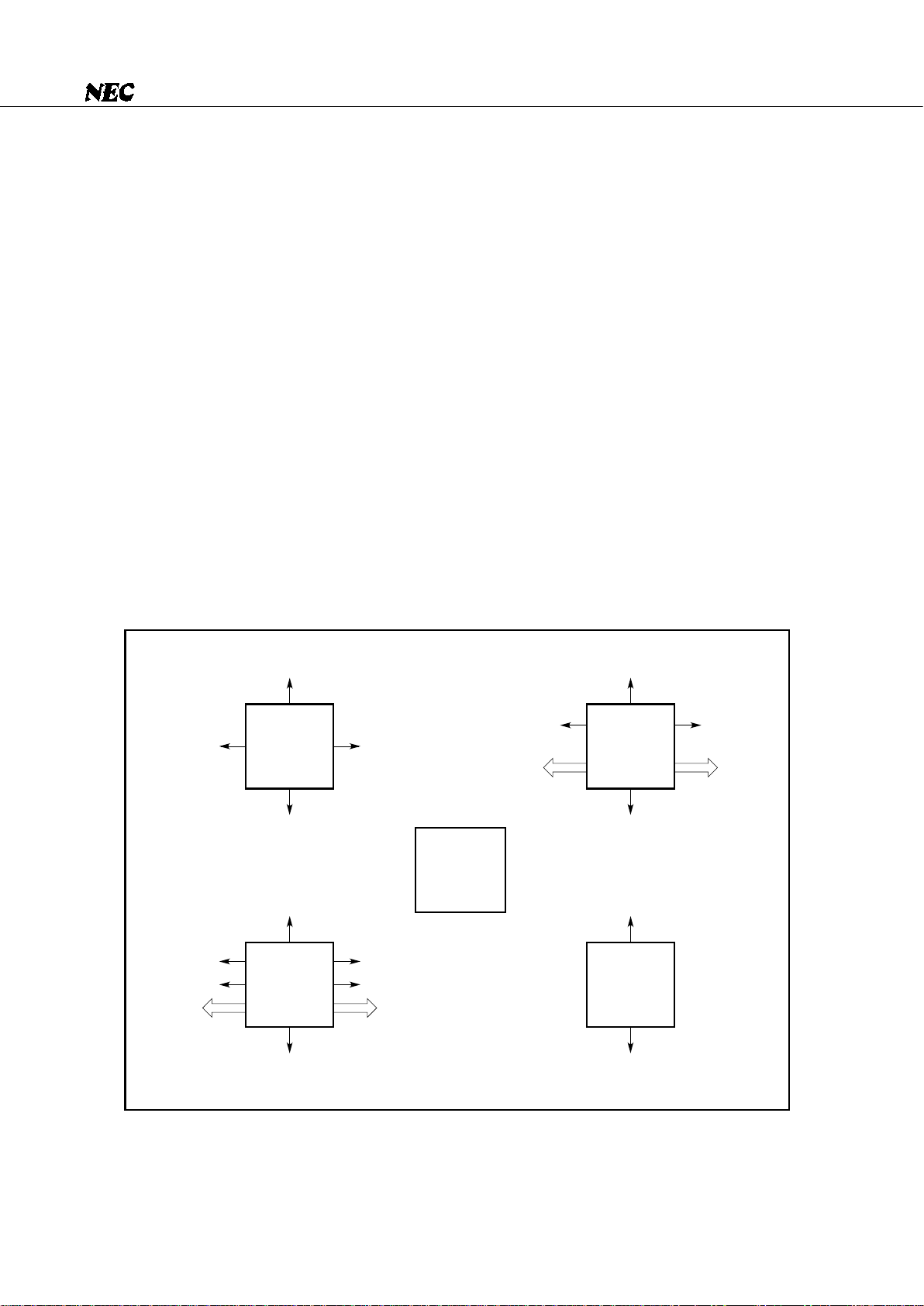
3.4 GENERAL REGISTERS: 8 × 4 BITS × 4 BANKS
The general registers are mapped to particular addresses in data memory. Four banks of registers are
provided, with each bank consisting of eight 4-bit registers (B, C, D, E, H, L, X, A).
The register bank (RB) to be enabled at the time of instruction execution is determined by
RB = RBE•RBS: (RBS = 0 to 3)
Each general register allows 4-bit manipulation. In addition, BC, DE, HL, or XA serves as a register pair
for 8-bit manipulation. DL also makes a register pair as well as DE and HL; these three register pairs can be
used as data pointers.
A general register area can be addressed and accessed as normal RAM, regardless of whether it is used
as a register.
Fig. 3-4 General Register Format Fig. 3-5 Register Pair Format
03
C
03
B
03
E
03
D
03
L
03
H
03
A
03
X
Address
000H
001H
002H
003H
004H
005H
006H
007H
008H
00FH
010H
017H
018H
01FH
A register
X register
L register
H register
E register
D register
C register
B register
Same as bank 0
Same as bank 0
Same as bank 0
·································
Data memory
03
Register bank 0
Register bank 1
Register bank 2
Register bank 3
Page 32

32
µ
PD75517(A)
3.5 ACCUMULATORS
In the
µ
PD75517(A), the A register and the XA register pair function as accumulators. The A register is mainly
used for 4-bit data processing instructions, and the XA register pair is mainly used for 8-bit data processing
instructions.
For a bit manipulation instruction, the carry flag (CY) functions as a bit accumulator.
Fig. 3-6 Accumulators
3.6 STACK POINTER (SP) AND STACK BANK SELECT REGISTER (SBS)
The
µ
PD75517(A) uses static RAM as stack memory (LIFO scheme), and the 8-bit register holding the start
address of the stack area is the stack pointer (SP).
The stack area is located at addresses 000H to 3FFH in memory banks 0, 1, 2, and 3. Either of the memory
banks is selected according to the value of the 2-bit SBS. (See Table 3-1.)
Table 3-1 Stack Area to Be Selected by the SBS
The SP is decremented before a write (save) operation to stack memory, and is incremented after a read
(restoration) operation from stack memory. The SBS is set with a 4-bit memory manipulation instruction. Note
that the high-order two bits are always set to 00.
Fig. 3-8 and 3-9 show data saved to and restored from stack memory in these stack operations.
To place the stack area at a given location, the SP can be initialized with an 8-bit memory manipulation
instruction, and the SBS can be initialized with a 4-bit memory manipulation instruction. Both can be read
from as well.
When the SP is initialized to 00H, a stack operation starts at the high-order address (nFFH) of memory bank
(n) specified with the SBS.
A stack area must be within the memory bank specified with the SBS. If a stack operation exceeds address
n00H, the operation returns to address nFFH of the same bank. Stacking beyond memory bank boundaries
is enabled only by resetting the SBS.
A RESET signal occurrence causes the contents of the SP and the SBS to be undefined, so that the SP must
always be initialized to a desired value at the start of the program.
Bit accumulator
4-bit accumulator
8-bit accumulator
CY
A
AX
SBS2
0
1
0
1
SBS
Memory bank 0
Memory bank 1
Memory bank 2
Memory bank 3
Stack area
- - - - - - - - - - - - - - - - - - - -
SBS1
0
0
1
1
Page 33

33
µ
PD75517(A)
Fig. 3-7 Stack Pointer and Stack Bank Select Register Formats
Example SP initialization
In this example, stack area is allocated in memory bank 2 and stack operation starts at address
2FFH.
SEL MB15 ; or CLR1 MBE
MOV A, #2
MOV SBS, A ; Specify memory bank 2 as a stack area
MOV XA, #00H
MOV SP, XA ; SP ← 00H
SP
SP
SP
SP
SP7 SP6 SP5 SP4 SP3 SP2 SP1 0
SBS0SBS100
SP
SBS
Symbol
F80H
F84H
Address
SBS
0FFH
100H
000H
1FFH
200H
2FFH
300H
3FFH
Memory bank 0
Memory bank 1
Memory bank 2
Memory bank 3
Page 34

34
µ
PD75517(A)
Fig. 3-8 Data Saved to Stack Memory
Fig. 3-9 Data Restored from Stack Memory
Note A PSW other than the MBE or RBE is not saved/restored.
Remark Data marked with * is undefined.
SP – 6
0
SP – 4 PC3 - PC0
PC7 - PC4
SP – 2 IST1
CY
SP
SP – 5
SP – 3
SP – 1
Stack
PC14 PC13
PC12
IST0
SK2
MBE
SK1
RBE
SK0
Interrupt
PSW
SP – 6
PC11 - PC8
0
SP – 2
SP
SP – 5
SP – 1
Stack
PC14 PC13
PC12
CALL, CALLA, or CALLF instruction
SP – 2
Lower bits of pair register
Upper bits of pair register
SP
SP – 1
Stack
PUSH instruction
SP – 4 PC3 - PC0
PC7 - PC4SP – 3
**
MBE
RBE
***
*
PC11 - PC8
Note
SP
0
SP + 2 PC3 - PC0
PC7 - PC4
SP + 4 IST1
CY
SP + 6
SP + 1
SP + 3
SP + 5
Stack
PC14 PC13
PC12
IST0
SK2
MBE
SK1
RBE
SK0
RETI instruction
PSW
SP
PC11 - PC8
0
SP + 4
SP + 6
SP + 1
SP + 5
Stack
PC14 PC13
PC12
RET or RETS instruction
SP
Lower bits of pair register
Upper bits of pair register
SP + 2
SP + 1
Stack
POP instruction
SP + 2 PC3 - PC0
PC7 - PC4SP + 3
**
MBE
RBE
***
*
PC11 - PC8
Note
Page 35

35
µ
PD75517(A)
3.7 PROGRAM STATUS WORD (PSW): 8 BITS
The program status word (PSW) consists of various flags closely associated with processor operations.
The PSW is mapped to addresses FB0H and FB1H in the data memory space. The four bits at address FB0H
can be manipulated with a memory manipulation instruction.
Fig. 3-10 Program Status Word Format
Table 3-2 PSW Flags Saved/Restored in Stack Operation
RBEMBEIST0IST1SK0SK1SK2CY
Address
Can be manipulated
by an instruction
specifically provided
for controlling this flag
Cannot be manipulated Can be manipulated
Symbol
PSW
FB1H FB0H
When CALL, CALLA, or CALLF instruction is executed
When hardware interrupt occurs
When RET or RETS instruction is executed
When RETI is executed
Save
Restore
MBE and RBE are saved.
All PSW bits are saved.
MBE and RBE are restored.
All PSW bits are restored.
Saved/restored flag
Page 36

36
µ
PD75517(A)
(1) Carry flag (CY)
The carry flag is a 1-bit flag used to store overflow or underflow occurrence information when an arithmetic
operation with a carry (ADDC, SUBC) is executed.
The carry flag also has the function of a bit accumulator, and therefore can be used to store the result of
a Boolean operation performed on the CY and bit at a specified data memory bit address.
The carry flag is manipulated using special instructions, independently of the other PSW bits.
A RESET signal occurrence causes the carry flag to be undefined.
Table 3-3 Carry Flag Manipulation Instructions
Remark mem*.bit represents the following three addressing modes:
• fmem.bit
• pmem.@L
• @H+mem.bit
Example Bit 3 at address 3FH is ANDed with P33, then the result is output to P50.
MOV H, #3H ; Set high-order 4 bits in register H
MOV1 CY, @H+0FH.3 ; CY ← Bit 3 at 3FH
AND1 CY, PORT3.3 ; CY ← CY P33
MOV1 PORT5.0, CY ; P50 ← CY
(2) Skip flags (SK2, SK1, SK0)
The skip flags are used to store skip status, and are automatically set or reset when the CPU executes an
instruction.
The user cannot directly manipulate these flags as operands.
(3) Interrupt status flag (IST1, IST0)
The interrupt status flag is a 2-bit flag used to store the status of processing being performed. (For detailed
information, see Table 5-3.)
Instruction dedicated to
carry flag manipulation
Bit transfer instruction
Bit Boolean instruction
Interrupt handling
SET1 CY
CLR1 CY
NOT1 CY
SKT CY
MOV1 mem*.bit,CY
MOV1 CY,mem*.bit
AND1 CY,mem*.bit
OR1 CY,mem*.bit
XOR1 CY,mem*.bit
Interrupt execution
RETI
- - - - - - - - - - - - - - - - - - - - - - - - - - - - - - - - - - - - - - - - - - - - - - - - - - - - - - - - - - - - - - - - - - -
Sets CY to 1.
Clears CY to 0.
Inverts the contents of CY.
Skips if CY is set to 1.
Transfers the contents of CY to a specified bit.
Transfers the contents of a specified bit to CY.
ANDs, ORs, or XORs CY with the contents of a specified bit, then
sets the result in CY.
Saves CY and all other PSW bits to stack memory in parallel.
Restores CY together with the other PSW bits from stack memory.
Carry flag operation/processingInstruction (mnemonic)
∨
Page 37

37
µ
PD75517(A)
Table 3-4 Information Indicated by the Interrupt Status Flag
The interrupt priority control circuit (see Fig. 5-1) checks this flag to control multiple interrupts.
The contents of the IST1 and IST0 are saved as part of the PSW to stack memory if an interrupt is accepted,
then are automatically set to a one-step higher status. The RETI instruction restores the contents present
before an interrupt occurs.
The interrupt status flag can be manipulated using a memory manipulation instruction, and the status of
processing being performed can be changed by program control.
Caution The user must always disable interrupts with the DI instruction before manipulating this flag,
and must enable interrupts with the EI instruction after manipulating this flag.
(4) Memory bank enable flag (MBE)
The memory bank enable flag is a 1-bit flag used to specify the address information generation mode for
the high-order four bits of a 12-bit data memory address.
When the MBE is set to 1, the data memory address space is expanded, allowing all data memory space
to be addressed.
When the MBE is reset to 0, the data memory address space is fixed, regardless of MBS setting. (See Fig.
2-1.)
A RESET signal occurrence automatically initializes the MBE by setting the MBE to the content of bit 7
at program memory address 0.
In vectored interrupt processing, the MBE is automatically set to the content of bit 7 in the vector address
table for servicing the interrupt.
Usually, the MBE is set to 0 in interrupt processing, and static RAM in memory bank 0 is used.
(5) Register bank enable flag (RBE)
The register bank enable flag is a 1-bit flag used to determine whether to expand the general register bank
configuration.
When the RBE is set to 1, a set of general registers can be selected from register banks 0 to 3, depending
on the setting of the register bank select register (RBS).
When the RBE is reset to 0, register bank 0 is always selected as general registers, regardless of the setting
of the RBS.
A RESET signal occurrence automatically initializes the RBE by setting the RBE to the content of bit 6 at
program memory address 0.
When a vectored interrupt occurs, the RBE is automatically set to the content of bit 6 in the vector address
table for servicing the interrupt. Usually, the RBE is set to 0 in interrupt processing. Register bank 0 is
used for 4-bit processing, and register banks 0 and 1 are used for 8-bit processing.
Normal program processing is being performed.
Any interrupts are acceptable.
A lower- or higher-priority interrupt is being serviced.
Higher-priority interrupts are acceptable.
A higher-priority interrupt is being serviced.
No interrupts are acceptable.
Not to be set
IST1
IST0
0
0
1
1
0
1
0
1
Status 0
Status 1
Status 2
—
Status of processing
being performed
Processing and interrupt control
Page 38

38
µ
PD75517(A)
3.8 BANK SELECT REGISTER (BS)
The bank select register consists of a register bank select register (RBS) and memory bank select register
(MBS), which specify a register bank and memory bank to be used, respectively.
The RBS and MBS are set using the SEL RBn instruction and SEL MBn instruction, respectively.
The contents of BS can be saved to or restored from a stack area eight bits at a time by using the PUSH
BS/POP BS instruction.
Fig. 3-11 Bank Select Register Format
(1) Memory bank select register (MBS)
The memory bank select register is a 4-bit register used to store the high-order four bits of a 12-bit data
memory address. The contents of this register specify a memory bank to be accessed. Note, however,
that the
µ
PD75517(A) allows only memory banks 0, 1, 2, 3, and 15 to be specified.
The MBS is set with the SEL MBn instruction (n = 0, 1, 2, 3, 15)
Fig. 2-1 shows the range of addressing using MBE and MBS settings.
A RESET signal occurrence initializes the MBS to 0.
(2) Register bank select register (RBS)
The register bank select register specifies a register bank to be used as general registers; a register bank
can be selected from register banks 0 to 3.
The RBS is set with the SEL RBn instruction (n = 0 to 3).
A RESET signal occurrence initializes the RBS to 0.
Table 3-5 Register Bank to Be Selected with the RBE and RBS
Remark ×: Don’t care
Symbol
BS
MBS3 MBS2 MBS1 MBS0 0 0 RBS1 RBS0
F83H
MBS
F82H
RBS
Address
Bank 0 is always selected.
Bank 0 is selected.
Bank 1 is selected.
Bank 2 is selected.
Bank 3 is selected.
RBS
RBE
Register bank
Always 0
0
1
3
0
0
2
0
0
1
×
0
0
1
1
0
×
0
1
0
1
Page 39

39
µ
PD75517(A)
4. PERIPHERAL HARDWARE FUNCTIONS
4.1 DIGITAL I/O PORTS
The
µ
PD75517(A) employs memory-mapped I/O, enabling all I/O ports to be mapped to data memory space.
Fig. 4-1 Data Memory Address Assigned to Digital Port
Table 4-1 lists the I/O port manipulation instructions. These instructions provide a wide range of control
including 8-bit I/O and bit manipulation as well as 4-bit I/O.
Examples 1. Test the state of P13, then output different values to ports 4 and 5 according to the test result.
SKT PORT1.3 ; Skip if bit 3 of port 1 is 1
MOV XA, #18H ; XA ← 18H
Consecutive
MOV XA, #14H ; XA ← 14H
SEL MB15 ; or CLR1 MBE
OUT PORT4, XA ; Ports 5 and 4 ← XA
2. SET1 PORT4.@L ; Set the bit of ports 4 to 7 specified by the L register to 1
P03 P02 P01 PORT 0FF0H P00
3210 SymbolAddress
P13 P12 P11 PORT 1FF1H P10
P23 P22 P21 PORT 2FF2H P20
P33 P32 P31 PORT 3FF3H P30
P43 P42 P41 PORT 4FF4H P40
P53 P52 P51 PORT 5FF5H P50
P63 P62 P61 PORT 6FF6H P60
P73 P72 P71 PORT 7FF7H P70
P83 P82 P81 PORT 8FF8H P80
P93 P92 P91 PORT 9FF9H P90
P103 P102 P101 PORT 10FFAH P100
P113 P112 P111 PORT 11FFBH P110
P123 P122 P121 PORT 12FFCH P120
P133 P132 P131 PORT 13FFDH P130
P143 P142 P141 PORT 14FFEH P140
P153 P152 P151 PORT 15FFFH P150
Page 40

40
µ
PD75517(A)
Table 4-1 I/O Pin Manipulation Instructions
Notes 1. Before an instruction is executed, MBE must be set to 0, or MBS must be set to 15 when MBE
is 1.
2. The lower 2 bits of an address and a bit address are specified indirectly with the L register.
Port Port Port Port Port Port Port Port Port Port Port Port Port Port Port Port
0 1 2 3 4 5 6 7 8 9 10 11 12 13 14 15
IN A, PORTn
Note 1
❍
IN XA, PORTn
Note 1
——❍❍————
OUT PORTn.A
Note 1
—— ❍ — ❍ —
OUT PORTn.XA
Note 1
——❍❍————
SET1 PORTn.bit — — ❍ — ❍ —
SET1 PORTn.@L
Note 2
—— ❍ — ❍ —
CLR1 PORTn.bit — — ❍ — ❍ —
CLR1 PORTn.@L
Note 2
—— ❍ — ❍ —
SKT PORTn.bit ❍
SKT PORTn.@L
Note 2
❍
SKF PORTn.bit ❍
SKF PORTn.@L
Note 2
❍
MOV1 CY, PORTn.bit ❍
MOV1 CY, PORTn.@L
Note 2
❍
MOV1 PORTn.bit, CY — — ❍ — ❍ —
MOV1 PORTn.@L, CY
Note 2
—— ❍ — ❍ —
AND1 CY, PORTn.bit ❍
AND1 CY, PORTn.@L
Note 2
❍
OR1 CY, PORTn.bit ❍
OR1 CY, PORTn.@L
Note 2
❍
XOR1 CY, PORTn.bit ❍
XOR1 CY, PORTn.@L
Note 2
❍
Page 41

41
µ
PD75517(A)
(1) Types, features, and configurations of digital I/O ports
Table 4-2 lists the types of digital I/O ports.
Fig. 4-2 through 4-8 present the configurations of the ports.
Table 4-2 Types and Features of Digital Ports
Note This port can directly drive the LED.
P10 is also used as an external vectored interrupt input pin. This input is provided with a noise eliminator.
(See Section 5.2 for details.)
The use of pull-up resistors can be specified for ports 0 (excluding pin P00/INT4), 1 to 3, 6, and 7 by software.
Also used as INT4, SCK0, SO0/
SB0, and SI0/SB1.
Also used as INT0 to INT2, and
TI0.
Also used as PTO0, PCL, and BUZ.
—
The use of pull-up resistors can
be specified by mask options in
units of bits.
Also used as KR0 to KR3.
Also used as KR4 to KR7.
Also used as PPO, SCK1, SO1,
and SI1.
The use of a pull-down resistor
can be specified by a mask option in units of bits.
—
The use of pull-up resistors can
be specified by mask options in
units of bits.
Also used as AN4 to AN7.
Port name
Function
Operation and feature
Remarks
PORT0
PORT1
PORT2
PORT3
Note
PORT4
Note
PORT5
Note
PORT6
PORT7
PORT8
PORT9
PORT10
PORT11
PORT12
PORT13
PORT14
PORT15
4-bit input
4-bit I/O
4-bit I/O (N-channel open-drain 10 V)
4-bit I/O
4-bit input
4-bit I/O
4-bit I/O
4-bit I/O (N-channel open-drain 10 V)
4-bit input
Allows read and test at any time regardless of
the operation modes of dual function pins.
Allows input or output mode setting in units
of 4 bits.
Allows input or output mode setting in units
of 1 or 4 bits.
Allows input or output
mode setting in units
of 4 bits.
Allows input or output
mode setting in units
of 1 or 4 bits.
Allows input or output
mode setting in units
of 4 bits.
Allows read and test at any time regardless of
the operation modes of dual function pins.
Allows input or output mode setting in units
of 4 bits.
Allows input or output mode setting in units
of 4 bits.
Allows input or output mode setting in units
of 4 bits.
Allows read and test at any time regardless of
the operation modes of dual function pins.
Ports 4 and 5 may be
paired, allowing data
I/O in units of 8 bits.
Ports 6 and 7 may be
paired, allowing data
I/O in units of 8 bits.
Page 42

42
µ
PD75517(A)
(2) Setting the I/O mode
As shown in Fig. 4-9, the I/O mode for each I/O port is set with the port mode register.
Each port functions as an input port when the corresponding bit of the port mode register is set to 0, and
functions as an output port when the same bit is set to 1.
An 8-bit memory manipulation instruction is used to set port mode register group A, B, or C.
The generation of a RESET signal clears all the bits of each port mode register to 0. This means that the
output buffers are set off and all ports function in the input mode.
Page 43

43
µ
PD75517(A)
Fig. 4-2 Configuration of Ports 0, 1, and 8
Internal bus
8 CSIM0
Selector Selector
P01
output
latch
Internal
SCK0
SI0 SCK0 SO0INT4
V
DD
Pull-up
resistor
P-ch
P00/INT4
P01/SCK0
P02/SO0/SB0
P03/SI0/SB1
Bit 0 of
POGA
Input buffer
Output buffer which can
be switched to either
push-pull output or N-ch
open-drain output
Pull-up
resistor
V
DD
P-ch
P10/INT0
P11/INT1
P12/INT2
P13/TI0
Bit 1 of
POGA
Input buffer
Φ or f
X
/64
Noise elimination
circuit
Input buffer with hysteresis
TI0 INT2 INT1 INT0
Input buffer
8
CSIM1
P80/PPO
P81/SCK1
P82/SO1
P83/SI1
SI1
SO1 SCK1 Internal SCK1 PPO
Page 44

44
µ
PD75517(A)
Fig. 4-3 Configuration of Ports 3n and 6n (n = 0 to 3)
Fig. 4-4 Configuration of Ports 2 and 7
Internal bus
Bit m of
POGA
Pull-up
resistor
P-ch
V
DD
Pmn
Input buffer
MPX
PMmn = 0
PMmn = 1
PMmn
Output latch
Bit of port mode register
group A
Output buffer
m = 3, 6
n = 0 to 3
Internal bus
Input buffer
MPX
Pm0
Pm1
Pm2
Pm3
PMm = 0
PMm = 1
PMm
Output
latch
Output
buffer
Bit of port mode
register group B or C(m = 2, 7)
P-ch
Bit m of
POGA
V
DD
Pull-up
resistor
Page 45

45
µ
PD75517(A)
Fig. 4-5 Configuration of Ports 4, 5, 12, 13, and 14
Internal bus
Input buffer
MPX
V
DD
Pm0
Pm1
Pm2
Pm3
PMm = 0
PMm = 1
PMm
Output
latch
Pull-up resistor
(mask option)
Open-drain
output
buffer
Port mode registers
Bit of the group B (m = 4, 5): Ports 4 and 5
Bit of the group C (m = 4, 5, 6): Ports 12, 13, and 14
Page 46

46
µ
PD75517(A)
Fig. 4-6 Configuration of Port 9
Internal bus
Bit 1 of port mode
register group C
PM9
Output
latch
Input buffer
Output buffer
MPX
PM9 = 1
PM9 = 0
P90
P91
P92
P93
Pull-down resistors
(mask option)
Page 47

47
µ
PD75517(A)
Fig. 4-7 Configuration of Ports 10 and 11
Fig. 4-8 Configuration of Port 15
Internal bus
AN4/P150
AN5/P151
AN6/P152
AN7/P153
Input instruction
Input buffer
To A/D converter
Internal bus
Input buffer
MPX
Pm0
Pm1
Pm2
Pm3
PMm = 0
PMm = 1
PMm
Output
latch
CMOS output buffer
Bit of port mode
register group C (m = 10, 11)
Page 48

48
µ
PD75517(A)
Fig. 4-9 Formats of Port Mode Registers
(a) Port mode register group A
(b) Port mode register group B
(c) Port mode register group C
Note To develop a program, these bits must be set to 0. They correspond to PM8 and PM15. While this
chip is an input-only device, an emulator has I/O ports.
PM63 PM62 PM61 PM60 PM33 PM31PM32 PM30
76543 120
FE8H
Address
PMGA
Symbol
P30 I/O specification
P31 I/O specification
P32 I/O specification
P33 I/O specification
P60 I/O specification
P61 I/O specification
P62 I/O specification
P63 I/O specification
PM14 PM13 PM12 PM11 PM9PM10
76543 120
FEEH
Address
PMGC
Symbol
Port 9 (P90 - P93) I/O specification
Port 10 (P100 - P103) I/O specification
Port 11 (P110 - P113) I/O specification
Port 12 (P120 - P123) I/O specification
Port 13 (P130 - P133) I/O specification
Port 14 (P140 - P143) I/O specification
0
1
Input mode (Output buffer off)
Output mode (Output buffer on)
Contents of specification
PM7 PM5 PM4 PM2
76543 120
FECH
Address
PMGB
Symbol
Port 2 (P20-P23) I/O specification
Port 4 (P40-P43) I/O specification
Port 5 (P50-P53) I/O specification
Port 7 (P70-P73) I/O specification
————
—
Note
—
Note
Page 49

49
µ
PD75517(A)
(3) Operation of digital I/O ports
When an instruction is executed, the operation of the port and pins depends on the I/O mode setting, as
listed in Table 4-3.
Table 4-3 I/O Port Operations by I/O Instructions
Note Instruction such as SET1 PORTn.bit or CLR1 PORTn.bit
Receives data on certain pins.
Transfers data in the accumulator to
the output latch.
The contents of the output latch are
undefined.
When a 1-bit test instruction,
4-, or 8-bit instruction is
executed
When a 4-, 8-bit output
instruction is executed
When a 1-bit output
instruction
Note
is executed
Receives the contents of the output
latch.
Outputs data in the accumulator to
output pins.
Changes the output pin state
according to the instruction.
Input mode corresponding bit in
the mode register is 0
[Output buffer is off]
Input mode corresponding bit in
the mode register is 1
[Output buffer is on]
Page 50

50
µ
PD75517(A)
(4) Use of pull-up and pull-down resistors
Ports 0 (excluding pin P00/INT4), 1 to 3, 6, and 7 can be provided with pull-up resistors by software.
Ports 4, 5, and 12 to 14 can be provided with pull-up resistors by mask options. Port 9 can also be provided
with pull-down resistors by mask options.
Table 4-4 Specifying the Use of Pull-Up and Pull-Down Resistors
Note The P00 pin cannot be provided with a pull-up resistor.
Fig. 4-10 Format of the Register Group A Specifying the Use of Pull-Up Resistors
PO7 PO6 — — PO3 PO1PO2 PO0
76543 120
FDCH
Address
POGA
Symbol
0
1
No built-in pull-up resistor provided
Built-in pull-up resistor provided
Specification contents
Port 0 (P01 - P03)
Port 1 (P10 - P13)
Port 2 (P20 - P23)
Port 3 (P30 - P33)
Port 6 (P60 - P63)
Port 7 (P70 - P73)
Port (pin name) Specifying the use of pull-up and pull-down resistor Bit in POGA
The use of pull-up resistors is specified in units of 3 bits
by software.
The use of pull-up resistors is specified in units of 4 bits
by software.
The use of pull-up resistors is specified in units of bits
by mask options.
The use of pull-down resistors is specified in units of bits
by mask options.
bit 0
bit 1
bit 2
bit 3
bit 6
bit 7
—
—
Port 0 (P01-P03)
Note
Port 1 (P10-P13)
Port 2 (P20-P23)
Port 3 (P30-P33)
Port 6 (P60-P63)
Port 7 (P70-P73)
Port 4 (P40-P43)
Port 5 (P50-P53)
Port 12 (P120-P123)
Port 13 (P130-P133)
Port 14 (P140-P143)
Port 9 (P90-P93)
Page 51

51
µ
PD75517(A)
4.2 CLOCK GENERATOR
(1) Configuration of the clock generator
The clock generator supplies various clock signals to the CPU and peripheral hardware. Fig. 4-11 shows
the configuration of the clock generator.
Fig. 4-11 Block Diagram of the Clock Generator
Note Instruction execution
Remarks 1. fX : Main system clock frequency
2. f
XT : Subsystem clock frequency
3. PCC : Processor clock control register
4. SCC: System clock control register
Subsystem
clock generator
Main system
clock generator
Clock timer
•
Basic interval timer (BT)
•
Timer/event counter
•
Serial interface
•
Clock timer
•
Clock output circuit
•
A/D converter
1/8 to 1/4096
Frequency divider
Selec-
tor
Selec-
tor
Frequency
divider
CPU
clock
Φ
Oscillator
disable
signal
Internal bus
HALT
Note
STOP
Note
PCC2, PCC3
clear signal
Wait release signal from BT
Standby release signal from
interrupt control circuit
RESET signal
XT1
XT2
X1
X2
4
SCC
SCC3
SCC0
PCC
PCC0
PCC1
PCC2
PCC3
STOP F/F
QS
R
HALT F/F
S
Q
R
f
XT
f
X
1/2 1/16
1/4
1/4
Timer/pulse
generator
Page 52

52
µ
PD75517(A)
(2) Functions of the clock generator
The clock generator generates the clock signals listed below, and controls the standby mode and other
CPU operation modes.
• Main system clock fX
• Subsystem clock fXT
• CPU clock Φ
• Clocks for peripheral hardware
The operation of the clock generator is determined by the processor clock control register (PCC) and
system clock control register (SCC). The clock generator functions and operates as described below.
(a) The generation of a RESET signal selects the lowest-speed mode
Note 1
for the main system clock.
(PCC = 0, SCC = 0)
(b) When the main system clock is selected, the PCC can be set to select one of four CPU clocks
Note 2
.
(c) When the main system clock is selected, the two standby modes, STOP mode and HALT mode, are
available.
(d) The SCC can be set to select the subsystem clock for very low-speed, low-current operation (122
µ
s:
at 32.768 kHz). In this case, the PCC set value does not affect the CPU clock signal.
(e) When the subsystem clock is selected, main system clock generation can be stopped with the SCC.
In addition, the HALT mode can be used, but the STOP mode cannot be used. (Subsystem clock
generation cannot be stopped.)
(f) Clocks for peripheral hardware are produced by dividing the main system clock signal. Only to the
watch timer, the subsystem clock can be directly supplied so that the watch and buzzer output
functions can operate continuously even in a standby mode.
(g) When the subsystem clock is selected, the watch timer can operate normally, but other hardware
cannot be used because they operate with the main system clock.
Notes 1. 10.7
µ
s (at 6.0 MHz) or 15.3 µs (at 4.19 MHz)
2. 0.67
µ
s, 1.33 µs, 2.67 µs, 10.7 µs (at 6.0 MHz), or 0.95 µs, 1.91 µs, 3.82 µs, 15.3 µs (at 4.19 MHz)
Page 53

53
µ
PD75517(A)
(3) Processor clock control register (PCC)
The PCC is a 4-bit register for selecting a CPU clock with the low-order two bits and for selecting a CPU
operation mode with the high-order two bits. (See Fig. 4-12.)
When bit 3 or bit 2 is set to 1, the standby mode is set. When this is released by the standby release signal,
these bits are automatically cleared to return to the normal operation mode. (See Chapter 6 for detailed
information.)
A 4-bit memory manipulation instruction is used to set the low-order two bits of the PCC. (The high-order
two bits are set to 0.)
Bit 3 and bit 2 are set to 1 using the STOP instruction and HALT instruction, respectively.
The STOP instruction and HALT instruction can be executed regardless of MBE setting.
A CPU clock can be selected only when the main system clock is used for operation. When the subsystem
clock is selected for operation, the low-order two bits of the PCC are invalidated, and f
XT/4 is automatically
set. The STOP instruction can be executed only when the main system clock is used for operation.
The generation of a RESET signal clears the PCC to 0.
Examples 1. The machine cycle is set to 0.95
µ
s (at 4.19 MHz).
SEL MB15
MOV A, #0011B
MOV PCC, A
2. The STOP mode is set. (A STOP instruction or HALT instruction must always be followed
by an NOP instruction.)
STOP
NOP
Page 54

54
µ
PD75517(A)
Fig. 4-12 Format of the Processor Clock Control Register
Remarks 1. fX : Output frequency from the main system clock oscillator
2. fXT: Output frequency from the subsystem clock oscillator
Address
FB3H
3210
PCC3 PCC2 PCC1 PCC0
Symbol
PCC
CPU clock selection bit
Operation with fx = 6.0 MHz
( ) indicates f
X
= 6.0 MHz
CPU clock frequency
Φ = f
X
/64 (93.7 kHz)
1 machine cycle 1 machine cycle
SCC = 0
( ) indicates f
XT
= 32.768 kHz
SCC = 1
CPU clock frequency
Φ = f
XT
/4 (8.192 kHz)
Φ = f
X
/16 (375 kHz) 2.67 s Not to be set
Φ = f
X
/8 (750 kHz)
Φ = f
X
/4 (1.5 MHz)
1.33 s
0.67 s
µ
µ
Φ = fXT/4 (8.192 kHz) 122 s
µ
122 s
µ
00
10
01
11
Operation with fX = 4.19 MHz
( ) indicates f
X
= 4.19 MHz
CPU clock frequency
Φ = f
X
/64 (65.5 kHz)
1 machine cycle 1 machine cycle
SCC = 0
( ) indicates f
XT
= 32.768 kHz
SCC = 1
CPU clock frequency
Φ = f
XT
/4 (8.192 kHz)
Φ = f
X
/16 (262 kHz)
Φ = f
X
/8 (524 kHz)
Φ = f
X
/4 (1.05 MHz)
1.91 s
15.3 s
µ
µ
122 s
µ
00
10
01
11
Φ = fXT/4 (8.192 kHz) 122 s
µ
Normal operation mode
HALT mode
STOP mode
Not to be set
00
10
01
11
CPU operation mode control bits
10.7 s
µ
µ
3.82 s
µ
0.95 s
µ
Not to be set
µs
µs
µs
µs
µs
µs
µs
µs
µs
µs
µs
µs
Page 55

55
µ
PD75517(A)
(4) System clock control register (SCC)
The SCC is a 4-bit register for selecting CPU clock Φ with the least significant bit and for controlling the
termination of main system clock generation with the most significant bit. (See Fig. 4-13.)
SCC.0 and SCC.3 are located at the same data memory address, but both bits cannot be changed at the
same time. Accordingly, SCC.0 and SCC.3 are set using bit manipulation instructions. SCC.0 and SCC.3
can be manipulated regardless of MBE setting.
Main system clock generation can be terminated by setting SCC.3 only when the subsystem clock is used
for operation. The STOP instruction must be used for generation termination when the main system clock
is used for operation.
The generation of a RESET signal clears the SCC to 0.
Fig. 4-13 Format of the System Clock Control Register
Cautions 1. A time period of up to 1/f
XT is needed to change the system clock. This means that to
terminate main system clock generation, SCC.3 must be set when the machine cycles
indicated in Table 4-5 or more have elapsed after the clock is switched from the main system
clock to the subsystem clock.
2. When the main system clock is used for operation, setting SCC.3 to stop clock generation
does not enter the normal STOP mode.
3. When SCC.3 is set to 1, the X1 input pin is connected to V
SS (GND electric potential) to
prevent leakage in the crystal oscillator. When an external clock is used as the main system
clock, never set SCC.3 to 1.
4. When the four bits of PCC are set to 0001B (Φ = f
X /16), do not set SCC.0 to 1. Before switching
the main system clock to the subsystem clock, be sure to manipulate the PCC bits so other
than 0001B is set. When the system operates on the subsystem clock, the PCC bits must
also be other than 0001B.
Address
FB7H SCC3
——
SCC0
Symbol
SCC
CPU clock frequency
Main system clock
Main system clock operation
Subsystem clock
Can oscillate
Subsystem clock
00
10
01
11
Oscillation stopped
SCC0SCC3
Not to be set
Page 56

56
µ
PD75517(A)
(5) System clock oscillator
The main system clock oscillator operates with a crystal (6.0 MHz standard) or ceramic resonator
connected to the X1 and X2 pins.
An external clock can also be input.
Fig. 4-14 External Circuitry for the Main System Clock Oscillator
(a) Crystal/ceramic oscillation (b) External clock
The subsystem clock oscillator operates with a crystal resonator (32.768 kHz standard) connected to the
XT1 and XT2 pins.
An external clock can also be input.
Fig. 4-15 External Circuitry for the Subsystem Clock Oscillator
(a) Crystal oscillation (b) External clock
A caution on connecting the oscillator is described on the next page.
X1
X2
PD75517(A)
X1
X2
PD75517(A
)
Crystal
oscillator
or ceramic
oscillator
External
clock
µµ
XT1
XT2
PD75517(A)
XT1
XT2
PD75517(A)
External
clock
32.768 kHz
Open
µµ
Page 57

57
µ
PD75517(A)
Caution When the main system clock or subsystem clock oscillator is used, conform to the following
guidelines when wiring at the shaded portions of Fig. 4-14 and 4-15 to eliminate the influence
of the wiring capacity.
• The wiring must be as short as possible.
• Other signal lines must not run in these areas. Any line carrying a high fluctuating current
must be kept away as far as possible.
• The grounding point of the capacitor of the oscillator must have the same potential as that
of V
SS. It must not be grounded to ground patterns carrying a large current.
• No signal must be taken from the oscillator.
When the subsystem clock is used, pay special attention to its wiring; the subsystem clock
oscillator has low amplification to minimize current consumption and is more likely to
malfunction due to noise than the main system clock oscillator.
Page 58

58
µ
PD75517(A)
(6) Time required to change the system clock and CPU clock
The system clock and CPU clock can be changed by using the least significant bit of the SCC and the loworder two bits of the PCC. This switching is not performed immediately after the contents of the registers
are rewritten, but the system operates with the previous clock for some machine cycles. Accordingly, after
this time period, the STOP instruction must be executed or SCC.3 must be set to 1 to terminate main system
clock generation.
Table 4-5 Maximum Time Required to Change the System Clock and CPU Clock
Remarks 1. Time enclosed in parentheses is required when f
X = 6.0 MHz and fXT = 32.768 kHz.
2. ×: Don’t care
3. CPU clock Φ is supplied to the CPU. The reciprocal of this frequency is a minimum instruction
time (defined as one machine cycle in this manual).
Caution When the four bits of PCC are set to 0001B (Φ = f
X/16), do not set SCC.0 to 1. Before switching
the main system clock to the subsystem clock, be sure to manipulate the PCC bits so other than
0001B is set. When the system operates on the subsystem clock, the PCC bits must also be
other than 0001B.
PCC1
0
PCC00SCC00PCC1
0
PCC0
1
SCC00PCC1
1
PCC00SCC00PCC1
1
PCC0
1
SCC01PCC1
×
PCC0
×
Setting before
switching
Setting after switching
0
1
1 machine cycle
8 machine cycles
16 machine cycles
Not to be set
1 machine cycle
4 machine cycles
16 machine cycles
1 machine cycle
1 machine cycle
4 machine cycles
8 machine cycles
1 machine cycle
4 machine cycles
8 machine cycles
16 machine cycles
1 machine cycle
SCC0
0
fX /64fXT machine
cycles
(3 machine cycles)
Not to be set
fX/8fXT machine
cycles
(23 machine cycles)
fX/4fXT machine
cycles
(46 machine cycles)
PCC
0
PCC
1
SCC
0
0
1
0
1
×
0
0
1
1
×
Page 59

59
µ
PD75517(A)
(7) Procedure for changing the system clock and CPU clock
The procedure for changing the system clock and CPU clock is explained using Fig. 4-16.
Fig. 4-16 Changing the System Clock and CPU Clock
1 The generation of a RESET signal starts CPU operation at the lowest speed of the main system
clock
Note 1
after a wait time
Note 2
for stable oscillation.
2 The PCC is rewritten for highest-speed operation after a time elapse which is sufficient for the voltage
on the VDD pin to be high enough for highest-speed operation.
3 The removal of commercial power is detected using, for example, an interrupt input (INT4 is useful),
then SCC.0 is set to operate with the subsystem clock. (In this case, the start of subsystem clock
generation must be confirmed beforehand.) After a time (32 machine cycles) required to switch to
the subsystem clock elapses, SCC.3 is set to terminate main system clock generation.
4 After detecting the input of commercial power by using an interrupt, SCC.3 is cleared to start main
system clock generation. After a time required for stable generation, SCC.0 is cleared to operate at
highest speed.
Notes 1. 10.7
µ
s (at 6.0 MHz) or 15.3 µs (at 4.19 MHz)
2. 21.8 ms (at 6.0 MHz) or 31.3 ms (at 4.19 MHz)
ON
OFF
Commercial
power
line voltage
V
DD
pin voltage
RESET signal
System clock
CPU clock
Wait (31.3 ms)
f
X
= 4.19 MHz
f
XT
= 32.768 kHz
f
X
15.3 s
µ
f
X
0.95 s
µ
f
XT
122 s
µ
f
X
0.95 s
µ
Internal reset
operation
Page 60

60
µ
PD75517(A)
4.3 CLOCK OUTPUT CIRCUIT
(1) Configuration of the clock output circuit
Fig. 4-17 shows the configuration of the clock output circuit.
(2) Functions of the clock output circuit
The clock output circuit outputs a clock pulse signal on the P22/PCL pin for remote control or for supplying
clock pulses to a peripheral LSI device.
The procedure for outputting a clock pulse signal is as follows:
(a) Select a clock output frequency, and disable clock output.
(b) Write a 0 in the P22 output latch.
(c) Set the output mode for port 2.
(d) Enable clock output.
Fig. 4-17 Configuration of the Clock Output Circuit
Remark The clock output circuit is designed so that pulses with short widths do not appear in enabling
or disabling clock output.
From the clock
generator
CLOM
Selector
Output
buffer
Port 2 input/
output mode
specification bit
P22 output
latch
PCL/P22
Internal bus
4
Φ
f
X
/23
fX/24
fX/26
PORT2.2 Bit 2 of PMGB
CLOM0CLOM10CLOM3
Page 61

61
µ
PD75517(A)
(3) Clock output mode register (CLOM)
The CLOM is a 4-bit register to control clock output.
The CLOM is set with a 4-bit memory manipulation instruction. No read operation is allowed on this
register.
Example CPU clock Φ is output on the PCL/P22 pin.
SEL MB15 ; or CLR1 MBE
MOV A, #1000B
MOV CLOM, A
The generation of a RESET signal clears the CLOM to 0, disabling clock output.
Fig. 4-18 Format of the Clock Output Mode Register
Caution Be sure to write a 0 in bit 2 of the CLOM.
Address
FD0H
3210
CLOM0
Symbol
CLOM
Φ Output
Note
(1.05 MHz, 524 kHz, 262 kHz, 65.5 kHz)
Output f
X
/23 (524 kHz)
Output f
X
/24 (262 kHz)
0
0
1
0
0
1
1
1
CLOM10CLOM3
Output f
X
/26 (65.5 kHz)
(Frequency when fX = 4.19 MHz)
Note Φ is the CPU clock supply selected by PCC.
0
1
Output disable
Output enable
Clock output enable/disable bit
Φ Output
Note
(1.50 MHz, 750 kHz, 375 kHz, 93.7 kHz)
Output f
X
/23 (750 kHz)
Output f
X
/24 (375 kHz)
Output fX/26 (93.7 kHz)
Clock output frequency selection bit
(Frequency when f
X
= 6.0 MHz)
0
0
1
0
0
1
1
1
Page 62

62
µ
PD75517(A)
(4) Application to remote control output
The clock output function of the
µ
PD75517(A) is applicable to remote control output. The frequency of
the carrier for remote control output is selected by the clock frequency select bit of the clock output mode
register. Pulse output is enabled or disabled by controlling the clock output enable/disable bit by software.
The clock output circuit is designed so that pulses with short widths do not appear in enabling or disabling
clock output.
Fig. 4-19 Application to Remote Control Output
PCL pin output
CLOM3
Page 63

63
µ
PD75517(A)
4.4 BASIC INTERVAL TIMER
(1) Configuration of the basic interval timer
Fig. 4-20 shows the configuration of the basic interval timer.
(2) Basic interval timer functions
The basic interval timer provides the following functions:
(a) Interval timer operation that generates a reference time interrupt
(b) Application of watchdog timer for detecting program crashes
(c) Selection of a wait time for releasing the standby mode, and counting
(d) Reading the count value
Fig. 4-20 Configuration of the Basic Interval Timer
Note Instruction execution
From the clock
generator
Internal bus
4
f
X
/25
fX/27
fX/29
fX/212
MPX
Basic interval timer
(8-bit frequency divider circuit)
Clear signal
Clear signal
BT interrupt
request flag
Vectored
interrupt
request
signal
IRQBT
Wait release
signal for standby
release
Set
signal
BT
8
BTM3BTM2BTM1BTM0BTM
SET1
Note
3
Page 64

64
µ
PD75517(A)
(3) Basic interval timer mode register (BTM)
BTM is a 4-bit register that controls operation of the basic interval timer.
The BTM contents are set by using a 4-bit memory manipulation instruction.
Bit 3 can be independently set using a bit manipulation instruction.
When bit 3 is set to 1, the contents of the basic interval timer are cleared, and the basic interval timer
interrupt request flag (IRQBT) is also cleared (to start the basic interval timer).
The generation of a RESET signal clears the contents to 0, and the longest interrupt request signal
generation interval time is set.
Examples 1. Set the interrupt generation interval to 1.95 ms (4.19 MHz).
SEL MB15 ; or CLR1 MBE
MOV A, #1111B
MOV BTM, A ; BTM ← 1111B
2. Clear BT and IRQBT (application of the watchdog timer)
SEL MB15 ; or CLR1 MBE
SET1 BTM.3 ; Set bit 3 of BTM to 1
Page 65

65
µ
PD75517(A)
Fig. 4-21 Format of the Basic Interval Timer Mode Register
Address
F85H
3210
BTM3 BTM2
BTM1
BTM0
Symbol
BTM
Input clock specification
00
10
11
0
1
0
111
When “1” is written to this bit, the basic interval timer operation starts (the counter
and the interrupt request flag are cleared).
When the operation starts, this bit is automatically reset to 0.
Basic interval timer start control bit
Interrupt interval time
(wait time for releasing standby)
fX/212
(1.02 kHz)
f
X
/29
(8.18 kHz)
f
X
/27
(32.768 kHz)
f
X
/25
(131 kHz)
2
20
/fX
(250 ms)
2
17
/fX
(31.3 ms)
2
15
/fX
(7.82 ms)
2
13
/f
X
(1.95 ms)
Not to be set
–
Input clock specification
00
10
11
0
1
0
111
Other
setting
Interrupt interval time
(wait time for releasing standby)
fX/212
(1.46 kHz)
f
X
/29
(11.7 kHz)
f
X
/27
(46.9 kHz)
f
X
/25
(188 kHz)
2
20
/fX
(175 ms)
2
17
/fX
(21.8 ms)
2
15
/fX
(5.46 ms)
2
13
/f
X
(1.37 ms)
Not to be set
–
(Frequency when f
X
= 6.0 MHz)
(Frequency when f
X
= 4.19 MHz)
Other
setting
Page 66

66
µ
PD75517(A)
(4) Operation of the basic interval timer
The basic interval timer (BT) is always incremented by the clock supplied from the clock generator, and
when it overflows, the interrupt request flag (IRQBT) is set. The count operation of BT cannot be stopped.
One of four interrupt generation intervals can be selected by setting BTM. (See Fig. 4-21.)
The basic interval timer and the interrupt request flag can be cleared by setting bit 3 of BTM to 1 (instruction
for starting as an interval timer).
The count status can be read by using an 8-bit manipulation instruction. No data can be loaded to the
timer.
Caution When reading the count value of the basic interval timer, execute a read instruction twice so
that unstable data which has been counted will not be read. If the two read values are
reasonable, use the second one as the result. If the two read values are far apart, retry from
the beginning.
Example Read the count value of BT.
SET1 MBE
SEL MB15
MOV HL, #BT ; Set the BT address in HL
LOOP: MOV XA, @HL ; First read
MOV BC, XA
MOV XA, @HL ; Second read
SKE XA, BC
BR LOOP
To allow the system clock to stabilize after releasing the STOP mode, a wait function is available which
stops the operation of the CPU until the basic interval timer overflows.
The wait time after generation of a RESET signal is fixed. On the other hand, a wait time can be selected
by setting BTM when releasing the STOP mode with an interrupt occurrence. In this case, the wait times
are the same as the interval times shown in Fig. 4-21. BTM must be set before the STOP mode is set. (For
details, see Chapter 6.)
Page 67

67
µ
PD75517(A)
4.5 CLOCK TIMER
(1) Clock timer
The µPD75517(A) contains one channel for a clock timer. Fig. 4-22 shows the configuration of the timer.
(2) Clock timer functions
(a) The clock timer sets the test flag (IRQW) every 0.5 seconds.
The standby mode can be released with IRQW.
(b) Either the main system clock or subsystem clock can produce 0.5-second intervals.
(c) The fast-forward mode produces an interval 128 times faster (3.91 ms), which is useful for program
debugging and testing.
(d) A fixed frequency (2.048 kHz) can be output to the P23/BUZ pin, so that it can be used for sounding
the buzzer and system clock frequency trimming.
(e) The frequency divider can be cleared, so the clock can start from zero seconds.
Caution When the main system clock operates at 6.0 MHz, a time interval of 0.5 s cannot be produced.
Before producing this time interval, the main system clock must be changed to the subsystem
clock.
Fig. 4-22 Block Diagram of the Clock Timer
Remark The values in parentheses are for f
X = 4.194304 MHz and fXT = 32.768 kHz
P23/BUZ
Internal bus
8
From the
clock
generator
f
X
128
(32.768 kHz)
f
XT
(32.768 kHz)
Selector Frequency divider
Selector
INTW
IRQW
set signal
2 Hz
0.5 sec
WM70000WM2WM1WM0
P23 output
latch
Bit 2 of PMGBPORT2.3
Output buffer
Clear signal
fW
(32.768 kHz)
Port 2 input/
output mode
WM
f
W
2
7
(256 Hz: 3.91 ms)
fW
2
14
fW
16
(2.048 kHz)
Page 68

68
µ
PD75517(A)
(3) Clock mode register
The clock mode register (WM) is an 8-bit register that controls the clock timer, and that is set with an
8-bit memory manipulation instruction. Fig. 4-23 shows the format.
The generation of a RESET signal clears all bits to 0.
Example Use the main system clock (4.19 MHz) for setting time, and enable buzzer output.
CLR1 MBE
MOV XA, #84H
MOV WM, XA ; Set WM
Fig. 4-23 Format of the Clock Mode Register
Address
F98H
Symbol
WM
0
WM0
1
WM1
2
WM2
3
0
4
0
5
0
6
0
7
WM7
WM0
0
1
Selects divided system clock output:
Selects subsystem clock: f
XT
Count clock (fW) selection bit
WM1
0
1
Normal clock mode ( : sets IRQW at 0.5 s)
Advanced clock mode ( : sets IRQW at 3.91 ms)
Operation mode selection bit
WM2
0
1
Disables clock operation (clears the frequency dividing circuit)
Enables clock operation
Clock operation enable/disable bit
f
W
2
14
fX
128
fW
2
7
WM7
0
1
Disables BUZ output
Enables BUZ output
BUZ output enable/disable bit
Page 69

69
µ
PD75517(A)
4.6 TIMER/EVENT COUNTER
(1) Configuration of the timer/event counter
The µPD75517(A) contains one channel of timer/event counter, which is configured as shown in Fig.
4-24.
(2) Functions of the timer/event counter
The timer/event counter has the following functions.
(a) Programmable interval timer operation
(b) Output of a square wave at a given frequency to the PTO0 pin
(c) Event counter operation
(d) Frequency divider operation that divides TI0 pin input by N and outputs the result to the PTO0 pin
(e) Supply of serial shift clock signal to a serial interface circuit
(f) Function of reading the state of counting
(3) Timer/event counter mode register (TM0) and timer/event counter output enable flag (TOE0)
The timer/event counter mode register (TM0) is an 8-bit register for controlling the timer/event counter.
Fig. 4-25 shows its format.
An 8-bit memory manipulation instruction is used to set the timer/event counter mode register.
Bit 3 is the timer start bit, and can be set independently of the other bits. Bit 3 is automatically reset to
0 when the timer starts operation.
Examples 1. The timer is started in the interval timer mode with CP = 4.09 kHz.
SEL MB15 ; or CLR1 MBE
MOV XA, #01001100B
MOV TM0, XA ; TM0 ← 4CH
2. The timer is restarted according to the setting of the timer/event counter mode register.
SEL MB15 ; or CLR1 MBE
SET1 TM0.3 ; TM0.bit3 ← 1
The generation of a RESET signal clears all bits to 0.
The timer/event counter output enable flag (TOE0) enables or disables output of the timer out F/F (TOUT
F/F) status to the PTO0 pin.
The timer out F/F (TOUT F/F) is inverted by a match signal transmitted from the comparator.
The timer out F/F is reset when an instruction sets bit 3 of the timer mode register (TM0).
The generation of a RESET signal clears the TOE0 and TOUT F/F to 0.
Page 70

70
µ
PD75517(A)
Fig. 4-24 Block Diagram of the Timer/Event Counter
Count register (8)
P13/
TI0
Note Instruction execution
MPX
Timer operation start signal
888
From the
clock
generator
Internal bus
TM06 TM05 TM04 TM03 TM02
PORT1.3
(See Fig. 4-11.)
Comparator (8)
Modulo register (8)
TO enable
flag
P20
output
latch
signal
Port 2
input/
output
mode
Clear signal
T0
TMOD0
Bit 2 of PGMB
P20/PTO0
Output
buffer
Reset
RESET
IRQT0 clear
signal
TOUT
F/F
TM0
SET1
Note
Input buffer
IRQT0
set signal
INTT0
PORT2.0TOE0
To serial
interface
CP
Match
8
8
Page 71

71
µ
PD75517(A)
Fig. 4-25 Format of the Timer/Event Counter Mode Register
Address
FA0H
76 5 4
—
Symbol
TM0
TM04TM06
—
—TM02TM03TM05
32 1 0
Operation mode
0
1
Count operation
Halts (retains
the contents of
counting)
Count
operation
Timer start specification bit
When “1” is written to this bit, the counter and the IRQT0
flag are cleared. Count operation starts if bit 2 has been
set to 1.
Count pulse (CP) select bit
(Frequency when f
X
= 6.0 MHz)
TM05
0
0
0
0
1
1
TM06
0
0
1
1
1
1
TM04
0
1
0
1
0
1
Count pulse (CP)
TI0 input rising edge
TI0 input falling edge
f
X
/210 (5.86 kHz)
fX/28 (23.4 kHz)
fX/26 (93.8 kHz)
fX/24 (375 kHz)
Other setting Not to be set
TM05
0
0
0
0
1
1
TM06
0
0
1
1
1
1
TM04
0
1
0
1
0
1
Count pulse (CP)
TI0 input rising edge
TI0 input falling edge
fX/210 (4.09 kHz)
fX/28 (16.4 kHz)
fX/26 (65.5 kHz)
fX/24 (262 kHz)
Other setting Not to be set
(Frequency when f
X
= 4.19 MHz)
Page 72

72
µ
PD75517(A)
Fig. 4-26 Format of the Timer/Event Counter Output Enable Flag
(4) Operation mode of the timer/event counter
The timer/event counter operates in the count operation disable mode or in the count operation mode,
depending on the setting of the mode register.
The following operations are possible, regardless of the setting of the mode register:
1 P13/TI0 pin signal input and test
2 Output of the timer out F/F status to the PTO0
3 Setting of the modulo register (TMOD0)
4 Reading from the count register (T0)
5 Setting, clearing, and testing of the interrupt request flag (IRQT0)
(a) Count operation disable mode
This mode is set when bit 2 of TM0 is set to 0. In this mode, count operation is not performed because
count pulse (CP) supply to the count register is stopped.
Address
FA2H TOE0
3
Timer/event counter output enable flag (W)
Disables
Enables
0
1
Page 73

73
µ
PD75517(A)
(b) Count operation mode
This mode is set when bit 2 of TM0 is set to 1. In this mode, a count pulse signal selected with bits
4 to 6 is supplied to the count register for count operation as shown in Fig. 4-28.
Timer operation is usually started in the following steps:
1 A count value is set in the modulo register (TMOD0).
2 An operation mode, count clock, and start instruction are set in the mode register (TM0).
An 8-bit data transfer instruction is used to set the modulo register.
Caution A value other than 0 must be set in the modulo register.
Example The value 3FH is set in the modulo register of channel 0.
SEL MB15 ; or CLR1 MBE
MOV XA, #3FH
MOV TMOD0, XA
If the value set in the modulo register matches the contents of the count register, the match signal
is generated. Then, the TOUT F/F is inverted, and the counter register is cleared.
The interval time of the generation of the match signal is calculated as follows:
(Set value of the modulo register + 1) × resolution
The resolution is 1/count pulse frequency.
Table 4-6 indicates the resolution and maximum set time (when FFH is set in the modulo register),
depending on a selected count pulse.
Table 4-6 Resolution and Maximum Set Time
(When f
X = 6.0 MHz)
(When fX = 4.19 MHz)
Mode register
TM04
0
1
0
1
TM06
1
1
1
1
TM05
0
0
1
1
Maximum set time
43.7 ms
10.9 ms
2.73 ms
683 µs
Resolution
171 µs
42.7 µs
10.7 µs
2.67 µs
Timer channel 0
Mode register
TM04
0
1
0
1
TM06
1
1
1
1
TM05
0
0
1
1
Maximum set time
62.5 ms
15.6 ms
3.91 ms
977 µs
Resolution
244 µs
61.1 µs
15.3 µs
3.81 µs
Timer channel 0
Page 74

74
µ
PD75517(A)
Fig. 4-27 Operation in the Count Operation Mode
Fig. 4-28 Timing of Count Operation
TI0
Count register
(T0)
Internal
clock
Comparator
Modulo register
(TMOD0)
TOUT
F/F
Clear
signal
Match
To CSI
(Only for channel 0)
PTO0
INTT0
(IRQT0 set signal)
CP
MPX
Match Match
Timer start specification
Reset
0 1 2 n – 1 n 0 1 2 n – 1
n
01234
n
Count register
Modulo register
Count pulse
(CP)
TOUT F/F
Page 75

75
µ
PD75517(A)
4.7 TIMER/PULSE GENERATOR
(1) Timer/pulse generator functions
The µPD75517(A) contains one channel for a timer/pulse generator that can be used as a timer or a pulse
generator. It has the following functions:
(a) Functions available when the timer/pulse generator is used in the timer mode
• 8-bit interval timer operation using one of five clock sources (occurrence of IRQTPG)
• Square wave output to the PPO pin
(b) Functions available when the timer/pulse generator is used in the PWM pulse generation mode
• PWM pulse output to the PPO pin with an accuracy of 14 bits (applicable for electronic tuning when
used as an D/A converter)
• Generation of interrupts at regular intervals (2
15
/fX)
Note
Note 215/fX = 5.46 ms (at 6.0 MHz) or 7.81 ms (at 4.19 MHz)
If pulse output is unnecessary, the PPO pin can be used as a 1-bit output port.
Caution If the timer/pulse generator is operating when the STOP mode is set, it may malfunction. So
the timer/pulse generator must be disabled with the mode register in advance.
Page 76

76
µ
PD75517(A)
(2) Timer/pulse generator mode register (TPGM)
The timer/pulse generator mode register (TPGM) is an 8-bit register that controls operation of the timer/
pulse generator. Fig. 4-29 shows the format of the register.
TPGM is set with an 8-bit memory manipulation instruction.
Bit 3 enables or disables the transfer (reloading) of the timer/pulse generator modulo register (MODH and
MODL) contents to the modulo latch. Bit 3 can be manipulated independently of the other bits.
By setting TPGM1 to 0, timer/pulse generator operation can be stopped to decrease current consumption.
The generation of a RESET signal clears all bits to 0.
Fig. 4-29 Format of Timer/Pulse Generator Mode Register
76543210
TPGM7 — TPGM5 TPGM4 TPGM3 0 TPGM1 TPGM0
Address
F90H
Symbol
TPGM
0
1
TPGM0
Select PWM pulse generation mode
Select timer mode
Timer/pulse generator operation mode selection bit
0
1
TPGM1
Disable timer/pulse generator operation
Enable timer/pulse generator operation
Timer/pulse generator operation enable/disable bit
0
1
TPGM3
Disable reloading of modulo register
Enable reloading of modulo register
Modulo register reload enable/disable bit
0
1
TPGM4
Output 0 to PPO output latch
Output 1 to PPO output latch
PPO output latch data
0
1
TPGM5
Static output on PPO pin
Pulse output (square wave/PWM) on PPO pin
PPO pin output selection bit static/pulse
0
1
TPGM7
Disable output on PPO pin (high-impedance)
Enable output on PPO pin
PPO pin output enable/disable bit
Page 77

77
µ
PD75517(A)
(3) Configuration and operation when the timer/pulse generator is used in the timer mode
Fig. 4-30 shows the configuration when the timer/pulse generator is used in the timer mode.
The timer mode is selected by setting bit 0 of TPGM to 1. In the timer mode, TPGM3 must be set to 1,
allowing a modulo register to be reloaded at any time.
In the timer mode, a prescaler is selected with the modulo register L (MODL), and a frequency or interrupt
interval value is set in the modulo register H (MODH). The timer starts when the TPGM1 is changed from
0 to 1.
Fig. 4-31 shows the operation timing for the MODH setting, and Table 4-7 shows the setting of a frequency
or interrupt interval.
The output to the PPO pin can be switched between the square wave output and static output. To output
a square wave, set TPGM5 and TPGM7 to 1.
Fig. 4-30 Block Diagram of the Timer/Pulse Generator (Timer Mode)
Internal bus
Modulo register L (8)
MODL
8
Modulo register H (8)
MODH
8
TPGM3
(Set to 1)
f
X
TPGM1
1/2
Frequency
divider
Prescaler select latch (5)
Modulo latch H (8)
Comparator (8)
Count register (8)
8
Clear
CP
Clear
Set
T F/F
Selec-
tor
TPGM4 TPGM5 TPGM7
INTTPG
IRQTPG
set signal
Output
buffer
PPO
Match
8
Page 78

78
µ
PD75517(A)
Example Set IRQTPG every 1.95 ms, and set the output high on the PPO pin.
CLR1 MBE ; or SEL MB15
MOV XA, #00100000B
MOV MODL, XA
MOV XA, #0FFH
MOV MODH, XA
MOV XA, #10011011B
MOV TPGM, XA ; Timer start, PPO ← 1
Caution When the timer operating in the timer operation mode is stopped, IRQTPG may be set because
T F/F is set. So, the timer must be stopped with an interrupt being disabled, then IRQTPG must
be cleared.
Example DI
CLR1 MBE
MOV XA, #0
MOV TPGM, XA
CLR1 IRQTPG
EI
Page 79

79
µ
PD75517(A)
Fig. 4-31 Timer Mode Operation Timing
Table 4-7 Modulo Register Settings
(When fX = 6.0 MHz)
(When f
X = 4.19 MHz)
Cautions 1. A value other than the above cannot be set in MODL. Bits 0, 1, and 7 must be set to 0.
2. N is the set value of MODH. 0 must not be set for N. Be sure to set a value from 1 to 255
for N.
N
0 1 2 N–1 N 0 0NN0
CP
T F/F
(PPO)
Count
register
MODH
Generate IRQTPG.Set TPGM1.
6
0
0
0
0
1
5
0
0
0
1
0
4
0
0
1
0
0
3
0
1
0
0
0
2
1
0
0
0
0
MODL bits 2-6
Interrupt generation interval
(fX = 6.0 MHz)
Square wave output frequency
(fX = 6.0 MHz)
256 (N+1)/fX = 85.3 µs - 10.9 ms
128 (N+1)/fX = 42.7 µs - 5.46 ms
64 (N+1)/fX = 21.3 µs - 2.73 ms
32 (N+1)/fX = 10.7 µs - 1.37 ms
16 (N+1)/fX = 5.33 µs - 683 µs
fX/256 (N+1) = 91.6 Hz - 11.7 kHz
fX/128 (N+1) = 183 Hz - 23.4 kHz
fX/64 (N+1) = 366 Hz - 46.9 kHz
fX/32 (N+1) = 732 Hz - 93.8 kHz
fX/16 (N+1) = 1465 Hz - 188 kHz
6
0
0
0
0
1
5
0
0
0
1
0
4
0
0
1
0
0
3
0
1
0
0
0
2
1
0
0
0
0
MODL bits 2-6
Interrupt generation interval
(fX = 4.19 MHz)
Square wave output frequency
(fX = 4.19 MHz)
256 (N+1)/fX = 122 µs - 15.6 ms
128 (N+1)/fX = 61.0 µs - 7.81 ms
64 (N+1)/fX = 30.5 µs - 3.91 ms
32 (N+1)/fX = 15.3 µs - 1.95 ms
16 (N+1)/fX = 7.63 µs - 977 µs
fX/256 (N+1) =64 Hz - 8 kHz
fX/128 (N+1) = 128 Hz - 16 kHz
fX/64 (N+1) = 256 Hz - 32 kHz
fX/32 (N+1) = 512 Hz - 65 kHz
fX/16 (N+1) = 1024 Hz - 131 kHz
Page 80

80
µ
PD75517(A)
(4) Configuration and operation when the timer/pulse generator is used in the PWM pulse generation mode
Fig. 4-32 shows the configuration when the timer/pulse generator is used in the PWM pulse generation
mode.
The PWM pulse generation mode is selected by setting TPGM0 to 0. TPGM5 and TPGM7 are set to 1 to
enable pulse output. In the PWM mode, the PWM pulse signal can be output on the PPO pin, and IRQTPG
can be set at intervals of a fixed time period (2
15
/fX = 5.46 ms: at 6.0 MHz or 215/fX = 7.81 ms: At 4.19 MHz).
PWM pulses output by the
µ
PD75517(A) are active-low and have an accuracy of 14 bits. This pulse signal
is applicable for electronic tuning and control of a DC motor when it is integrated by an external low-pass
filter and is converted to analog voltage. (See Fig. 4-33.)
The PWM pulse signal is generated by combining the basic period determined by 2
10
/fX and the secondary
period by 2
15
/fX so that the time constant of the external low-pass filter can be decreased.
Table 4-8 lists the basic and secondary periods by oscillator frequency.
Table 4-8 Basic and Secondary Periods
The low-level width of a PWM pulse depends on the 14-bit modulo latch value. The upper 8 bits of the
modulo latch are transferred from the 8 bits of MODH, and the lower 6 bits of the latch are transferred
from the upper 6 bits of MODL.
When the PWM pulse signal is converted to analog form, the voltage level of the analog output is obtained
as follows:
Value of modulo latch
V
AN = Vref ×
2
14
Vref: Reference voltage of external switching circuitry
To prevent an incorrect PWM pulse from being output by unstable modulo latch data being rewritten, the
µ
PD75517(A) allows correct data to be written in MODH and MODL beforehand with 8-bit manipulation
instructions, then in the 14-bit data which is to be transferred to the modulo latch at one time. This transfer
is referred to as reloading, and it is controlled by TPGM3. If TPGM3 is 0, reloading is disabled, and if it
is 1, reloading is enabled. Follow the procedure below to rewrite the modulo latch contents:
(i) Clear TPGM3 to disable reloading.
(ii) Change the MODH and MODL contents.
(iii) Set TPGM3 to enable reloading.
Cautions 1. If the modulo register H (MODH) is set to 0, the PWM pulse generator cannot function
normally. So be sure to set MODH to a value from 1 to 255.
2. If the lower 2 bits of the modulo register L (MODL) is read, the read result is unpredictable.
3. If the modulo latch is changed in a shorter period than the PWM pulse basic period
2
10
/fX (171 µs: at 6.0 MHz or 244 µs: at 4.19 MHz), PWM pulses do not change.
fX = 6.0 MHz
171 µs
5.46 ms
fX = 4.19 MHz
244 µs
7.81 ms
Basic period (210/fX)
Secondary period (215/fX)
Page 81

81
µ
PD75517(A)
Example Decrease analog output voltage to the lowest level, then increase it to the highest level.
CLR1 MBE
MOV XA, #01H
MOV MODH, XA ; MODH ← 01
MOV XA, #00H
MOV MODL, XA ; MODL ← 00
MOV XA, #10101010B
MOV TPGM, XA ; Enable PWM pulse output
•
•
•
•
•
•
•
•
•
CLR1 TPGM.3 ; Disable reloading
MOV XA, #0FFH
MOV MODH, XA
MOV XA, #0FCH
MOV MODL, XA
SET1 TPGM.3 ; Enable reloading
(5) Static output to the PPO pin
When pulse output is unnecessary, the PPO pin can be used as normal static output. In this case, the output
data is set in TPGM4 with TPGM5 being set to 0 and TPGM7 to 1.
Page 82

82
µ
PD75517(A)
Fig. 4-32 Block Diagram of the Timer/Pulse Generator (PWM Pulse Generation Mode)
Note At 4.19 MHz: 2
15
/fX = 7.81 ms
Fig. 4-33 Sample Configuration of D/A Conversion Using µPD75517(A)
Switching
circuit
Low-pass
filter
PWM
PPO
signal
V
AX
(analog voltage)
V
ref
PD75517 (A)
µ
Internal bus
Modulo register H (8)
MODH
8
TPGM3
f
X
TPGM1
1/2
PWM pulse generator
Selec-
tor
TPGM5 TPGM7
Output
buffer
PPO
Modulo register L (8)
MODL
8
Modulo latch (14)
MODH (8) MODL
7-2
(6)
INTTPG
(IRQTPG set signal)
(2
15
/fX = 5.46 ms: 6.0 MHz)
Note
Frequency
divider
Page 83

83
µ
PD75517(A)
4.8 SERIAL INTERFACE (CHANNEL 0)
The
µ
PD75517(A) has two channels of serial interface: Channel 0 and channel 1. Table 4-9 lists the
differences between channel 0 and channel 1.
Table 4-9 Differences between Channel 0 and Channel 1
Channel 1
Channel 0
Serial transfer mode, function
fX/24, fX/23, TOUT F/F, external clock
Start bit switchable: MSB/LSB
Serial transfer end interrupt request
flag (IRQCSI0)
Available
3-wire serial I/O
2-wire serial I/O
Serial bus interface (SBI)
Clock selection
Transfer method
Transfer end flag
fX/24, fX/23, external clock
Start bit: MSB
Serial transfer end flag (EOT)
Not available
Page 84

84
µ
PD75517(A)
4.8.1 Serial Interface (Channel 0) Functions
The clock synchronous 8-bit serial interface is contained in the
µ
PD75517(A) and has four modes.
The functions of the four modes are outlined below.
• Operation halt mode
This mode is used when serial transfer is not performed. This mode reduces power consumption.
• Three-wire serial I/O mode
In this mode, 8-bit data is transferred through three lines: Serial clock (SCK0), serial output (SO0), and serial
input (SI0).
The three-wire serial I/O mode allows full-duplex transmission, so data transfer can be performed at higher
speed.
The user can choose 8-bit data transfer starting with the MSB or LSB, so devices starting with either the
MSB or LSB can be connected.
The three-wire serial I/O mode enables connections to be made with the 75X series, 78K series, and many
other types of peripheral I/O devices.
• Two-wire serial I/O mode
In this mode, 8-bit data is transferred through two lines: Serial clock (SCK0) and serial data bus (SB0 or
SB1). By controlling output levels on the two lines by software, communication with multiple devices is
enabled.
The output levels of SCK0 and SB0 (or SB1) can be controlled by software, so the user can match an arbitrary
transfer format. This means that a line that has been required for handshaking to connect multiple lines
can be eliminated for more efficient I/O port utilization.
• Serial bus interface (SBI) mode
In this mode, communication with multiple devices can be performed using two lines: Serial clock (SCK0)
and serial data bus (SB0 or SB1).
This mode conforms to the NEC serial bus format.
In this mode, the transmitter can output, on the serial data bus, an address for selecting a device subject
to serial communication, commands directed to the remote device, and data. The receiver can identify an
address, commands, and data from received data by hardware. This function enables more efficient I/O
port utilization as in the case of the two-wire serial I/O mode. In addition, this function can simplify the
serial interface control portion of an application program.
4.8.2 Configuration of Serial Interface (Channel 0)
Fig. 4-34 shows the block diagram of the serial interface (channel 0).
Page 85

85
µ
PD75517(A)
Fig. 4-34 Block diagram of the Serial Interface (Channel 0)
Internal bus
88
8
8/4
P03/SI/SB1
P02/SO/SB0
P01/SCK0
(8)
fX/2
3
fX/2
4
fX/2
6
TOUT F/F
(from timer/event counter)
CSIM0
RELD
CMDD
ACKD
ACKT
ACKE
BSYE
RELT
CMDT
DQ
SET CLR
(8)
(8)
SBIC
Bit
test
Slave address register (SVA)
Address comparator
Shift register (SIO0)
Coincidence
signal
Bit manipulation
SO0 latch
Bit test
Selec-
tor
Selec-
tor
Busy/
acknowledge
output circuit
Bus release/
command/
acknowledge
detection circuit
Serial clock
counter
Serial clock
control circuit
INTCSI0
control circuit
IRQCSI0
set signal
INTCSI0
P01
output latch
MPX
External SCK0
Page 86

86
µ
PD75517(A)
4.8.3 Register Functions
(1) Serial operation mode register 0 (CSIM0)
Fig. 4-35 shows the format of serial operation mode register 0 (CSIM0).
CSIM0 is an 8-bit register which specifies a serial interface (channel 0) operation mode, serial clock, wakeup function, and so forth.
CSIM0 is manipulated using an 8-bit memory manipulation instruction. The higher three bits can be
manipulated bit by bit. Each bit can be manipulated using its name.
Each bit may or may not allow read and/or write operation. (See Fig. 4-35.) Bit 6 allows bit test operation
only; any data written to this bit is invalid.
When the RESET signal is input, this register is set to 00H.
Fig. 4-35 Format of Serial Operation Mode Register 0 (CSIM0) (1/3)
Remark (R) : Read only
(W): Write only
CSIE0 COI WUP CSIM04 CSIM03 CSIM01CSIM02 CSIM00
76543 120
Address
CSIM0
Symbol
Serial clock selection bit (W)
FE0H
Serial interface operation enable/disable specification bit (W)
Serial interface operation mode selection bit (W)
Wake-up function specification bit (W)
Signal from address comparator (R)
Page 87

87
µ
PD75517(A)
Fig. 4-35 Format of Serial Operation Mode Register 0 (CSIM0) (2/3)
Serial clock selection bit (W)
Note The values in parentheses are for f
X = 4.19 MHz or 6.0 MHz.
Serial interface operation mode selection bit (W)
Remark ×: Don’t care
Wake-up function specification bit (W)
Caution When WUP = 1 is set during BUSY signal output, BUSY is not released. In the SBI mode, the
BUSY signal is output until the next falling edge of the serial clock (SCK0) appears after release
of BUSY is directed. Before setting WUP = 1, be sure to confirm that the SB0 (or SB1) pin is high
after releasing BUSY.
Serial clock
SBI mode 2-wire serial I/O mode3-wire serial I/O mode
External clock applied to SCK0 pin
Time/event counter output (T0)
fX/24 (262 kHz or 375 kHz)
Note
fX/23 (524 kHz or 750 kHz)
Note
CSIM01 CSIM00
fX/26 (65.5 kHz or
93.8 kHz)
Note
SCK0 pin mode
0
0
1
1
0
1
0
1
Input
Output
Operation modeCSIM04 CSIM03 CSIM02
Bit sequence of
shift register 0
SIO07-0 ↔ XA
(Transfer starting
with MSB)
SIO00-7 ↔ XA
(Transfer starting
with LSB)
SIO07-0↔ XA
(Transfer starting
with MSB)
SIO07-0 ↔ XA
(Transfer starting
with MSB)
SI0 pin function
0
1
1
0
1
0
1
×
0
1
0
1
SO0 pin function
SO0/P02
(CMOS output)
SB0/P02
(N-ch open-drain
input/output)
P02 input
SB0/P02
(N-ch open-drain
input/output)
P02 input
SI0/P03
(Input)
P03 input
SB1/P03
(N-ch open-drain
input/output)
P03 input
SB1/P03
(N-ch open-drain
input/output)
3-wire serial I/O
mode
SBI mode
2-wire serial I/O
mode
Sets IRQCSI0 each time serial transfer is completed in each mode.
Used in the SBI mode only to set IRQCSI0 only when an address received after bus release matches
the data in the slave address register (wake-up state). SB0/SB1 goes to high-impedance state.
WUP
0
1
Page 88

88
µ
PD75517(A)
Fig. 4-35 Format of Serial Operation Mode Register 0 (CSIM0) (3/3)
Signal from address comparator (R)
Note COI can be read only before serial transfer is started or after serial transfer is completed. An
undefined value may be read during transfer.
COI data written by an 8-bit manipulation instruction is ignored.
Serial interface operation enable/disable specification bit (W)
Remarks 1. Each mode can be selected by setting CSIE0, CSIM03, and CSIM02.
2. The P01/SCK0 pin assumes the following state according to the setting of CSIE0, CSIM01, and
CSIM00:
Condition for being set (COI = 1)
When the slave address register (SVA) matches the
data of the shift register
COI
Note
Condition for being cleared (COI = 0)
When the slave address register (SVA) does not match
the data of the shift register
0
1
Serial clock counter
Cleared
Count operation
IRQCSI0 flag
Held
Can be set.
SO0/SB0, SI0/SB1 pin
Used only for port 0
Used in each mode as
well as for port 0
CSIE0
Shift register operation
Shift operation disabled
Shift operation enabled
CSIE0
0
1
1
1
CSIM03
×
0
1
1
CSIM02
×
×
0
1
Operation mode
Operation halt mode
Three-wire serial I/O mode
SBI mode
Two-wire serial I/O mode
CSIE0
0
1
0
0
0
1
1
1
CSIM01
0
0
1
0
1
1
0
1
CSIM00
0
0
0
1
1
0
1
1
P01/SCK0 pin state
Input port
High impedance
High level output
Serial clock output (High level output)
Page 89

89
µ
PD75517(A)
Remarks 3. When clearing CSIE0 during serial transfer, use the following procedure:
1 Disable interrupts by clearing the interrupt enable flag.
2 Clear CSIE0.
3 Clear the interrupt request flag.
Examples 1. f
X/2
4
is selected as the serial clock, serial interrupt IRQCSI0, is generated each time serial
transfer is completed, and serial transfer is performed in the SBI mode with the SB0 pin used
as the serial data bus.
SEL MB15 ; or CLR1 MBE
MOV XA, #10001010B
MOV CSIM0, XA ; CSIM0 ← 10001010B
2. Serial transfer dependent on the contents of CSIM0 is enabled.
SEL MB15 ; or CLR1 MBE
SET1 CSIE0
Page 90

90
µ
PD75517(A)
(2) Serial bus interface control register (SBIC)
Fig. 4-36 shows the format of the serial bus interface control register (SBIC).
SBIC is an 8-bit register consisting of bits for controlling the serial bus and flags for indicating the states
of input data from the serial bus. SBIC is used mainly in the SBI mode.
SBIC is manipulated using a bit manipulation instruction. SBIC cannot be manipulated using a 4-bit or
8-bit memory manipulation instruction.
Each bit may or may not allow read and/or write operation. (See Fig. 4-36.)
When the RESET signal is input, this register is set to 00H.
Caution Only the following bits can be used in the three-wire and two-wire serial I/O modes:
•
Bus release trigger bit (RELT): Sets the SO0 latch.
• Command trigger bit (CMDT): Clears the SO0 latch.
Fig. 4-36 Format of Serial Bus Interface Control Register (SBIC) (1/3)
Remark (R) : Read only
(W) : Write only
(R/W): Read/write
BSYE ACKD ACKE ACKT CMDD CMDTRELD RELT
76543 120
Address
SBIC
Symbol
Bus release trigger bit (W)
FE2H
Command trigger bit (W)
Bus release detection flag (R)
Command detection flag (R)
Acknowledge trigger bit (W)
Acknowledge enable bit (R/W)
Acknowledge detection flag (R)
Busy enable bit (R/W)
Page 91

91
µ
PD75517(A)
Fig. 4-36 Format of Serial Bus Interface Control Register (SBIC) (2/3)
Bus release trigger bit (W)
Caution Never clear SB0 (or SB1) during serial transfer. Be sure to clear SB0 (or SB1) before or after serial
transfer.
Command trigger bit (W)
Caution Never clear SB0 (or SB1) during serial transfer. Be sure to clear SB0 (or SB1) before or after serial
transfer.
Bus release detection flag (R)
Command detection flag (R)
Acknowledge trigger bit (W)
Cautions 1. Never set ACKT before or during serial transfer.
2. ACKT cannot be cleared by software.
3. Before setting ACKT, set ACKE = 0.
Acknowledge enable bit (R/W)
Control bit for bus release signal (REL) trigger output.
By setting RELT = 1, the SO0 latch is set to 1. Then the RELT bit is automatically cleared to 0.
RELT
Condition for being set (RELD = 1)
The bus release signal (REL) is detected.
RELD Condition for being cleared (RELD = 0)
1 The transfer start instruction is executed.
2 The RESET signal is entered.
3 CSIE0 = 0 (See Fig. 4-35.)
4 SVA does not match SIO0 when an address is
received.
Control bit for command signal (CMD) trigger output.
By setting CMDT = 1, the SO0 latch is cleared to 0. Then the CMDT bit is automatically cleared to 0.
CMDT
Condition for being set (CMDD = 1)
The command signal (CMD) is detected.
CMDD Condition for being cleared (CMDD = 0)
1 The transfer start instruction is executed.
2 The bus release signal (REL) is detected.
3 The RESET signal is entered.
4 CSIE0 = 0 (See Fig. 4-35.)
When set after transfer, ACK is output in phase with the next SCK0. After ACK signal output, this bit is automatically cleared to 0.
ACKT
Disables automatic output of the acknowledge signal (ACK). (Output by ACKT is possible.)ACKE
0
1
When set before transfer
When set after transfer
ACK is output in phase with the 9th clock of SCK0.
ACK is output in phase with SCK0 immediately following set
instruction execution.
Page 92

92
µ
PD75517(A)
Fig. 4-36 Format of Serial Bus Interface Control Register (SBIC) (3/3)
Acknowledge detection flag (R)
Busy enable bit (R/W)
Examples 1. A command signal is output.
SEL MB15 ; or CLR1 MBE
SET1 CMDT
2. RELD and CMDD are tested to identify the types of received data and the types of processing
accordingly.
By setting WUP = 1, this interrupt routine is processed only when an address match is found.
SEL MB15
SKF RELD ; RELD test
BR !ADRS
SKT CMDD ; CMDD test
BR !DATA
CMD :
• • • • • • • • • ; Command analysis
DATA :
• • • • • • • • • ; Data processing
ADRS :
• • • • • • • • • ; Address decode
Condition for being set (ACKD = 1)
The acknowledge signal (ACK) is detected (in phase
with the rising edge of SCK0).
ACKD Condition for being cleared (ACKD = 0)
1 The transfer start instruction is executed.
2 The RESET signal is entered.
1 The busy signal is automatically disabled.
2 Busy signal output is stopped in phase with the falling edge of SCK0 immediately after clear
instruction execution.
The busy signal is output after the acknowledge signal in phase with the falling edge of SCK0.
0
1
BSYE
Page 93

93
µ
PD75517(A)
(3) Shift register (SIO0)
Fig. 4-37 shows the configuration of peripheral hardware of shift register 0. SIO0 is an 8-bit register which
performs parallel-serial conversion and serial transfer (shift) operation in phase with the serial clock.
Serial transfer is started by writing data to SIO0.
In transmission, data written to SIO0 is output on the serial output (SO0) or serial data bus (SB0/SB1). In
reception, data is read from the serial input (SI0) or SB0/SB1 into SIO0.
Data can be read from or written to SIO0 by using an 8-bit manipulation instruction.
When the RESET signal is entered during operation, the value of SIO0 is undefined. When the RESET signal
is entered in the standby mode, the value of SIO0 is preserved.
Shift operation is stopped after 8-bit transmission or reception is completed.
Fig. 4-37 Peripheral Hardware of Shift Register 0
The timing for reading SIO0 and start of serial transfer (writing to SIO0) is as follows:
• When the serial interface operation enable/disable bit (CSIE0) = 1. However, the case where CSIE0 is
set to 1 after data is written to the shift register 0 is excluded.
• When the serial clock is masked after 8-bit serial transfer
• SCK0 is high.
DQ
SET
CLR
RELT
CMDT
CLK
BUSY/ACK
Internal bus
Address
comparator
Shift register (SIO0)
SO0 latch
Shift clock
N-ch open-drain output
CSIM0
Page 94

94
µ
PD75517(A)
(4) Slave address register (SVA)
The slave address register (SVA) has the two functions described below.
SVA is manipulated using an 8-bit manipulation instruction. SVA allows only write operation.
When the RESET signal is entered, the value of SVA is undefined. However, the value of SVA is preserved
when the RESET signal is entered in the standby mode.
• Slave address detection
[In the SBI mode]
SVA is used when the
µ
PD75517(A) is connected as a slave device to the serial bus. SVA is an 8-bit
register for a slave to set its slave address (number assigned to it). The master outputs a slave address
to the connected slaves to select a particular slave. Two data values (a slave address output from the
master and the value of SVA) are compared with each other by the address comparator. If a match
is found, the slave is selected.
At this time, bit 6 (COI) of serial operation mode register 0 (CSIM0) is set to 1.
Cautions 1. Slave selection or nonselection state is detected by detecting a match for a slave address
received after bus release (in the state of RELD = 1).
For this match detection, an address match interrupt (IRQCSI0) generated when WUP is set
to 1 is usually used. So detect selection/nonselection state by slave address when WUP
is set to 1.
2. When detecting selection/nonselection state without using an interrupt when WUP is 0,
do not use the address match detection method. Instead, use transfer of commands set
in advance in a program.
• Error detection
[In the two-wire serial I/O mode or SBI mode]
SVA detects an error in either of the following cases:
• When addresses, commands, or data is transferred with the
µ
PD75517(A) operating as the master
• When data is transferred with the
µ
PD75517(A) operating as a slave
4.8.4 Signals
Table 4-10 lists signals. Fig. 4-38 to 4-43 show operations of signals and flags.
Page 95

95
µ
PD75517(A)
Table 4-10 Various Signals (1/2)
SCK0
SB0 (SB1)
“H”
“H”
SCK0
SB0 (SB1)
Rising edge of SB0
(SB1) when SCK0 = 1
Falling edge of SB0
(SB1) when SCK0 = 1
Low level signal
output on SB0 (SB1)
during one SCK0 clock
cycle after serial
reception is completed
Low level signal
output on SB0 (SB1)
after acknowledge
signal
High level signal
output on SB0 (SB1)
before serial transfer
is started or after
serial transfer is
completed
Bus release signal
(REL)
Command signal
(CMD)
Acknowledge
signal
(ACK)
Busy signal
(BUSY)
Ready signal
(READY)
Output
device
Definition
• RELT is set.
• CMDT is set.
# ACKE = 1
$ ACKT is set.
• BSYE = 1
# BSYE = 0
$
Execution of
instruction to
write data to
SIO0 (Transfer
start request)
Condition for
output
• RELD is set.
• CMDD is clear-
ed.
• CMDD is set.
• ACKD is set.
Flag
operation
Meaning
of signal
Indicates that CMD
signal follows and
data transmitted is
address data.
(1)
(2)
Indicates completion
of reception.
Indicates that serial
transfer is disabled
because processing
is in progress.
Indicates that serial
transfar is enabled.
Signal name
Timing chart
READY
READY
ACK
SCK0
(SB1)
(SB1)
D0
D0
SB0
SB0
9
BUSY
ACK
BUSY
–
–
Master
Master
Master/
slave
Slave
Slave
Data transmitted
after REL signal
output is address.
(Data transmitted,
with REL signal
not being output,
is command.
1
2
1
2
Page 96

96
µ
PD75517(A)
Table 4-10 Various Signals (2/2)
Synchronous clock for
outputting address/
command/data, ACK
signal, synchronous
BUSY signal, and so on.
Address/command/data
is output during first 8
clock cycles.
8-bit data transferred in
phase with SCK0 after
REL signal and CMD
signal output
8-bit data transferred in
phase with SCK0 after
only CMD signal is
output, with REL signal
not being output
8-bit data transferred in
phase with SCK0, with
neither REL signal nor
CMD signal being
output
Serial clock
(SCK0)
Address
(A7 - A0)
Command
(C7 - C0)
Data
(D7 - D0)
Output
device
Definition
Execution of
instruction to
write data to SIO0
when CSIE0 = 1
(serial transfer
start request)
Note 2
Condition for
output
IRQCSI0 is set (on
rising edge of 9th
clock)
Note 1
Flag
operation
Meaning
of signal
Timing of signal
output on serial data
bus
Address of slave
device on serial bus
Directions and
messages to slave
device
Data processed by
slave or master
Signal name
Timing chart
Master
Master
Master
Master/
slave
Notes 1. When WUP = 0, IRQCSI0 is always set on the 9th rising edge of SCK0.
When WUP = 1, IRQCSI0 is set on the 9th rising edge of SCK0 only if a received address matches the value of the slave address register (SVA).
2. If the BUSY state is present, data transfer is started after the READY state is set.
SCK0
SB0
(SB1)
1278910
SCK0
SB0
(SB1)
12 78
SCK0
SB0
(SB1)
12 78
CMDREL
CMD
SCK0
SB0
(SB1)
12 78
Page 97

97
µ
PD75517(A)
Fig. 4-38 Operations of RELT, CMDT, RELD, and CMDD (Master)
Fig. 4-39 Operations of RELT, CMDT, RELD, and CMDD (Slave)
Fig. 4-40 Operation of ACKT
Caution Do not set the ACKT until the transfer is completed.
SIO0
SCK0
SB0 (SB1)
RELT
CMDT
RELD
CMDD
Transfer start request
SIO0
SCK0
12 78
D7 D6 D1 D0 SO0 latch
RELT
(Master)
CMDT
(Master)
RELD
CMDD
Transfer start request Write to SIO0.
When address match is found
When address mismatch is found
SCK0
6789
D2 D1 D0 SB0 (SB1) ACK
ACKT
ACK signal is output during first clock
cycle immediately after ACKT is set.
When set during this period
Page 98

98
µ
PD75517(A)
Fig. 4-41 Operation of ACKE
(a) When ACKE = 1 at time of transfer completion
(b) When ACKE is set after transfer completion
(c) When ACKE = 0 at time of transfer completion
(d) When ACKE = 1 period is too short
SCK0
12 78
D7 D6 D2 D1 SB0/SB1
D0
9
ACK
ACKE
When ACKE = 1 at this point
The ACK signal is output
during the ninth clock
cycle
SCK0
6789
D2 D1 D0SB0/SB1
ACK
ACKE
The ACK signal is output
during the first clock cycle
immediately after ACKT is set.
When ACKE is set during this period and ACKE = 1 at
the falling edge of the next SCK0
SCK0
12 78
D7 D6 D2 D1 SB0/SB1 D0
9
ACKE
The ACK signal is not
output
When ACKE = 0 at this point
SCK0
D2 D1 D0 SB0/SB1
ACKE
The ACK signal is not
output
When ACKE is set or cleared during this period,
and ACKE = 0 at the falling edge of SCK0
Page 99

99
µ
PD75517(A)
Fig. 4-42 Operation of ACKD
(a) When ACK signal is output during ninth SCK0 clock
(b) When ACK signal is output after ninth SCK0 clock
(c) Clear timing for case where start of transfer is requested during BUSY
Fig. 4-43 Operation of BSYE
SCK0
SB0/SB1
BSYE
9
BUSY
876
ACK
When BSYE = 1 at this point When reset operation is executed during
this period and BSYE = 0 at the falling edge
of SCK0.
SIO0
SCK0
D2 D1 D0 SB0/SB1
ACKD
9
ACK
876
Transfer start request
Transfer start
SIO0
SCK0
D2 D1 D0 SB0/SB1
ACKD
9
BUSY
876
D7 ACK
Transfer start request
D6
SIO0
SCK0
98
D2 D1 D0 SB0/SB1
ACKD
76
ACK
Transfer start request
Transfer start
Page 100

100
µ
PD75517(A)
4.8.5 Serial Interface (Channel 0) Operation
(1) Operation halt mode
The operation halt mode is used when serial transfer is not performed. This mode reduces power
consumption.
The shift register 0 does not perform shift operation in this mode, so the shift register can be used as a
normal 8-bit register. When the RESET signal is entered, the operation halt mode is set.
The P02/SO0/SB0 pin and P03/SI0/SBI pin function as input-only port pins. The P01/SCK0 pin can be used
as an input port pin by setting the serial operation mode register 0.
(2) Three-wire serial I/O mode operations
The three-wire serial I/O mode is compatible with other modes used in the 75X series,
µ
PD7500 series,
and 78K series.
Communication is performed using three lines: Serial clock (SCK0), serial output (SO0), and serial input
(SI0).
(a) Communication operation
The three-wire serial I/O mode transfers data, with eight bits as one block. Data is transferred bit by
bit in phase with the serial clock.
The shift register performs shift operation on the falling edge of the serial clock (SCK0). Transmit data
is latched on the SO0 latch, and is output on the SO0 pin. Receive data applied to the SI0 pin is latched
in the shift register 0 on the rising edge of SCK0.
When eight bits have been transferred, shift register 0 operation automatically terminates setting the
interrupt request flag (IRQCSI0).
Fig. 4-44 Timing of Three-Wire Serial I/O Mode
SCK0
SI0
IRQCSI0
1
SO0
23 4 5 6 7
8
DI0
DO0
DI1
DO1
DI2
DO2
DI3
DO3
DI4
DO4
DI5
DO5
DI6
DO6
DI7
DO7
Transfer is started in phase with falling edge of SCK0.
Execution of instruction that writes data to SIO0 (Transfer start request)
Completion of transfer
 Loading...