

Datasheet UPD75117HGK-XXX-8A8, UPD75117HGC-XXX-AB8, UPD75116HGK-XXX-8A8, UPD75116HGC-XXX-AB8 Datasheet (NEC)

© NEC Corporation 1994
DESCRIPTION
The µPD75117H is a 75X Series 4-bit single-chip microcomputer.
The
µ
PD75117H is a product which has the same functions as those of the µPD751××F, with the minimum
operating voltage reduced from the previous 2.7 V to 1.8 V, and achieving 1.91 µs operation at 1.8 V. Therefore, it facilitates low-voltage operation for a set requiring high-speed operation.
Functions are described in detail in the following User’s Manual, which should be read when carrying out
design work.
µ
PD75117H User’s Manual : IEU-799
FEATURES
• Memory capacity
ROM : 24448 × 8 bits (
µ
PD75117H)
: 16256 × 8 bits (
µ
PD75116H)
RAM : 768 × 4 bits
• High-speed low voltage operation
Minimum instruction execution time : 1.91
µ
s (VDD = 1.8 V)
0.95
µ
s (VDD = 2.7 V)
• Operating voltage range : 1.8 to 5.5 V (Ta = –40 to +60 °C)
• Input/output ports : 58
• Timer/counter : 3 channels
• Timer/event counter × 2 channels
• Basic interval timer × 1 channel
• 8-bit serial interface on chip
• Programmable threshold port : 4-bit resolution × 4 channels
• On-chip PROM product available :
µ
PD75P117H (One-time PROM)
APPLICATIONS
Cordless telephone subsets, portable radio equipment, pager, etc.
4-BIT SINGLE-CHIP MICROCOMPUTER
MOS INTEGRATED CIRCUIT
µ
PD75116H,75117H
DATA SHEET
Document No. IC-3120
(O.D.No. IC-8502)
Date Published May 1994P
Printed in Japan
The mark ★ shows major revised points.
"Unless there are any particular functional differences, the µPD75117H is described in this document as a
representative product."
The information in this document is subject to change without notice.
★
2
µ
PD75116H,75117H
ORDERING INFORMATION
Ordering Code Package Quality Grade
µ
PD75116HGC-×××-AB8 64-pin plastic QFP ( 14 mm) Standard
µ
PD75116HGK-×××-8A8 64-pin plastic QFP ( 12 mm) Standard
µ
PD75117HGC-×××-AB8 64-pin plastic QFP ( 14 mm) Standard
µ
PD75117HGK-×××-8A8 64-pin plastic QFP ( 12 mm) Standard
Remarks ×××: ROM code number
OVERVIEW OF FUNCTIONS
Contents
43
0.95 µs, 1.91 µs, 15.3 µs (4.19 MHz operation)
3-stage switching capability
24448 × 8 bits (µPD75117H), 16256 × 8 bits (µPD75116H)
768 × 4 bits
4 bits × 8 × 4 banks (memory mapping)
Total 58
• CMOS input pins : 10
• CMOS input/output pins : 32 (pins with LED direct drive
capability*1)
• N-ch open-drain input/output pins : 12 (pins with LED direct drive
capability*2)
(A pull-up resistor can be incorporated bit-wise.)
• Comparator input pins (4-bit precision) : 4
• 8-bit timer/event counter × 2
• 8-bit basic interval timer (watchdog timer applicable)
• 8 bits
• LSB-first/MSB-first switchable
• 2 transfer modes (transmission/reception and dedicated reception modes)
• External : 3
• Internal : 4
• External : 2
• STOP/HALT mode
• Various bit manipulation instructions (set, reset, test, Boolean operation)
• 8-bit data transfer, comparison, operation, increment/decrement instructions
• 1-byte relative branch instruction
• GETI instruction that can implement arbitrary 2-byte/3-byte instructions with 1
byte
• Bit manipulation memory (bit sequential buffer: 16 bits) on chip
• 64-pin plastic QFP ( 14 mm)
• 64-pin plastic QFP ( 12 mm)
Item
Basic instructions
Instruction cycle
On-chip memory
General register
Input/output port
Timer/counter
Serial interface
Vectored interrupt
Test input
Standby
Instruction set
Others
Package
ROM
RAM
*1. When VDD = 5 V, IOL = 15 mA.
2. When V
DD = 5 V, IOL = 10 mA.
★
★
★
3
µ
PD75116H,75117H
DIFFERENCES BETWEEN µPD75116H AND µPD75117H
µ
PD75116H
µ
PD75117H
16256 × 8 bits 24448 × 8 bits
(Mask ROM) (Mask ROM)
768 × 4 bits
No Yes
Memory bank 0 Memory banks 0, 1, 2
2-byte stack 3-byte stack
3 machine cycles 4 machine cycles
2 machine cycles 3 machine cycles
Undefined operation Normal operation
SBS register
Stack area
Item
ROM
RAM
Stack
Stack operation when subroutine call
instruction is executed
CALL instruction machine cycle
CALLF instruction machine cycle
BRA instruction
CALLA instruction
MOVT XA, BCDE
MOVT XA, BCXA
BR BCDE
BR BCXA
★

4
µ
PD75116H,75117H
CONTENTS
1. PIN CONFIGURATION (TOP VIEW) ...................................................................................................... 6
2. BLOCK DIAGRAM ................................................................................................................................... 8
3. PIN FUNCTIONS ..................................................................................................................................... 9
3.1 PORT PINS ....................................................................................................................................................... 9
3.2 OTHER PINS ..................................................................................................................................................... 10
3.3 PIN INPUT/OUTPUT CIRCUITS ..................................................................................................................... 11
3.4 RECOMMENDED CONNECTION OF UNUSED PINS ................................................................................... 12
4. MEMORY CONFIGURATION ................................................................................................................. 13
5. PERIPHERAL HARDWARE FUNCTIONS ............................................................................................... 18
5.1 PORT ................................................................................................................................................................. 18
5.2 CLOCK GENERATOR ....................................................................................................................................... 19
5.3 CLOCK OUTPUT CIRCUIT ............................................................................................................................... 20
5.4 BASIC INTERVAL TIMER ................................................................................................................................ 21
5.5 TIMER/EVENT COUNTER ............................................................................................................................... 21
5.6 SERIAL INTERFACE ......................................................................................................................................... 23
5.7 PROGRAMMABLE THRESHOLD PORT (ANALOG INPUT PORT) .............................................................. 25
5.8 BIT SEQUENTIAL BUFFER ............................................................................................................................. 26
6. INTERRUPT FUNCTION ........................................................................................................................ 27
7. STANDBY FUNCTION ............................................................................................................................ 29
8. RESET FUNCTION .................................................................................................................................. 30
9. INSTRUCTION SET ................................................................................................................................. 33
10. APPLICATION EXAMPLE ....................................................................................................................... 43
10.1 CORDLESS TELEPHONE (SUBSET) .............................................................................................................. 43
10.2 DISPLAY PAGER .............................................................................................................................................. 44
11. MASK OPTION SELECTION................................................................................................................... 45
12. ELECTRICAL SPECIFICATIONS ............................................................................................................. 46
13. PACKAGE INFORMATION ..................................................................................................................... 57
14. RECOMMENDED SOLDERING CONDITIONS ...................................................................................... 59
APPENDIX A. FUNCTIONAL DIFFERENCES AMONG µPD751×× SERIES PRODUCTS ......................... 60

5
µ
PD75116H,75117H
APPENDIX B. DEVELOPMENT TOOLS ........................................................................................................ 62
APPENDIX C. RELATED DOCUMENTS........................................................................................................ 63
6
µ
PD75116H,75117H
1
2
3
4
5
6
7
8
9
10
11
12
13
14
15
16
P41
P42
P43
P30
P31
P32
P33
V
DD
IC*
P140
P141
P142
P143
P130
P131
P132
P90
V
SS
P83
P82
P81
P80
P93
P92
P91
P13/INT3
P12/INT2
P11/INT1
P10/INT0
PTH03
PTH02
17 18 19 20 21 22 23 24 25 26 27 28 29 30 31 32
64 63 62 61 60 59 58 57 56 55 54 53 52 51 50 49
48
47
46
45
44
43
42
41
40
39
38
37
36
35
34
33
P70
P71
P72
P73
P60
P61
P62
P63X1X2
RESET
P50
P51
P52
P53
P40
PTH00
TI0
TI1
P23
P22/PCL
P21/PTO1
P20/PTO0
P03/SI
P02/SO
P01/SCK
P00/INT4
P123
P122
P121
P120
P133
PTH01
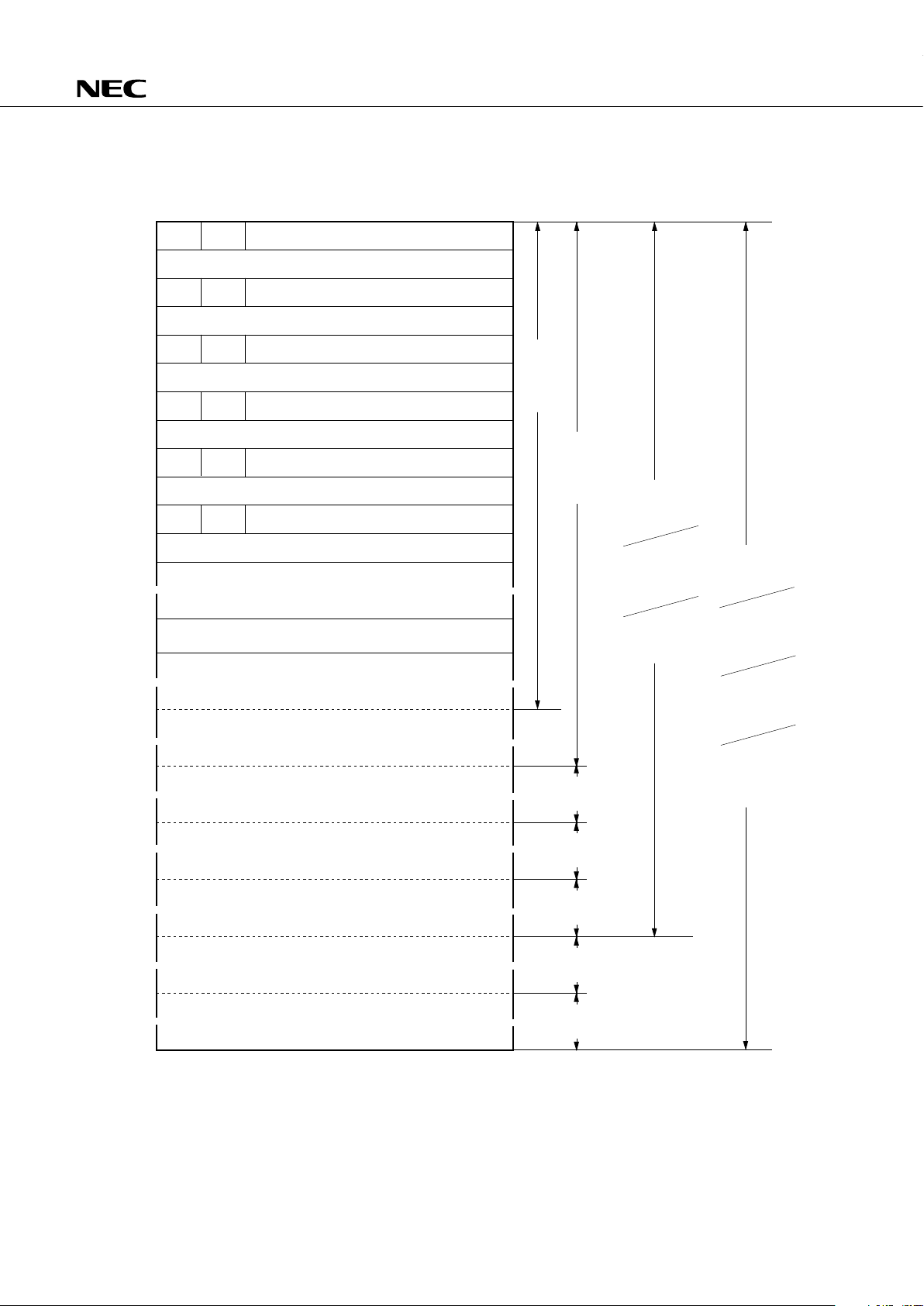
1. PIN CONFIGURATION (TOP VIEW)
* Connect the IC (Internally Connected ) pin to VDD directly.
µ
PD75116HGC-×××-AB8
µ
PD75116HGK-×××-8A8
µ
PD75117HGC-×××-AB8
µ
PD75117HGK-×××-8A8

7
µ
PD75116H,75117H
Pin Name
P00-P03 : Port 0 PCL : Programmable Clock Output
P10-P13 : Port 1 SCK : Serial Clock
P20-P23 : Port 2 SO : Serial Data Output
P30-P33 : Port 3 SI : Serial Data Input
P40-P43 : Port 4 PTH00-PTH03 : Programmable Treshold Input
P50-P53 : Port 5 INT0, INT1, INT4 : External Vectored Interrupt Input 0, 1, 4
P60-P63 : Port 6 INT2, INT3 : External Test Input 2, 3
P70-P73 : Port 7 X1, X2 : System Clock Oscillation 1, 2
P80-P83 : Port 8 RESET : Reset
P90-P93 : Port 9 V
DD : Positive Power Supply
P120-P123 : Port 12 V
SS : Ground
P130-P133 : Port 13 IC : Internally Connected
P140-P143 : Port 14
TI0, TI1 : Timer Input 0, 1
PTO0, PTO1 : Programmable Timer
Output 0, 1
8
µ
PD75116H,75117H
2. BLOCK DIAGRAM
*1. The µPD75116H program counter is composed of 14 bits.
2. The
µ
PD75117H incorporates the SBS register.
PORT 0
PORT 1
44P00-P03
P10-P13
PORT 3
PORT 4
PORT 5
PORT 6
4
4
4
4
PORT 2
4 P20-P23
P30-P33
P40-P43
P50-P53
P60-P63
PORT 7 4
P70-P73
SP(8)
BANK
GENERAL REG.
RAM
DATA
MEMORY
768 × 4 BITS
DECODE
AND
CONTROL
CY
ALU
PROGRAM
COUNTER (15) *1
ROM
PROGRAM
MEMORY
16256 × 8 BITS
: PD75116H
24448 × 8 BITS
: PD75117H
RESET
V
SS
STAND BY
CONTROL
V
DD
CPU CLOCK
CLOCK
GENERATOR
CLOCK
DIVIDER
CLOCK
OUTPUT
CONTROL
X2X1PCL/P22
f
X
/ 2
N
BASIC
INTERVAL
TIMER
INTER-
RUPT
CONTROL
INTT1
INTBT
PORT 14 4
P140-P143
PORT 12 4
P120-P123
TIMER/EVENT
COUNTER
#0
INTT0
TI0
PTO0/P20
TIMER/EVENT
COUNTER
#1
TI1
PTO1/P21
SERIAL
INTERFACE
INTSIO
SCK/P01
SO/P02
SI/P03
PROGRAM-
MABLE
THRESHOLD
PORT #0
PTH00-PTH03
INT4/P00
INT2/P12
INT1/P11
INT0/P10
INT3/P13
PORT 13 4
P130-P133
PORT 9 4
P90-P93
PORT 8 4
P80-P83
BIT SEQ.
BUFFER
(16)
SBS(2) *2
4
Φ
µ
µ
9
µ
PD75116H,75117H
3. PIN FUNCTIONS
3.1 PORT PINS
Dual-
Function Pin
INT4
SCK
SO
SI
INT0
INT1
INT2
INT3
PTO0
PTO1
PCL
—
—
—
—
—
—
—
—
—
—
—
I/O Circuit
Type *1
B
F
E
B
B
E
E
E
E
E
E
E
E
M
M
M
*1. : Schmitt trigger input
2. Direct LED drive capability (When V
DD = 5 V, IOL = 15 mA).
3. Direct LED drive capability (When VDD = 5 V, IOL = 10 mA).
4. Open-drain … high impedance
On-chip pull-up resistor … high level
*3
*3
*2
*2
*2
*2
*2
*2
*2
*2
*3
★
★
Pin Name
P00
P01
P02
P03
P10
P11
P12
P13
P20
P21
P22
P23
P30 to P33
P40 to P43
P50 to P53
P60 to P63
P70 to P73
P80 to P83
P90 to P93
P120 to P123
P130 to P133
P140 to P143
Input/Output
Input
Input/output
Input/output
Input
Input
Input/output
Input/output
Input/output
Input/output
Input/output
Input/output
Input/output
Input/output
Input/output
Input/output
Input/output
Function
4-bit input port (PORT 0).
4-bit input port (PORT 1).
4-bit input/output port (PORT 2).
Programmable 4-bit input/output port (PORT 3).
Input/output can be specified bit-wise.
4-bit input/output port (PORT 4).
4-bit input/output port (PORT 5).
Programmable 4-bit input/output port (PORT 6).
Input/output can be specified bit-wise.
4-bit input/output port (PORT 7).
4-bit input/output port (PORT 8).
4-bit input/output port (PORT 9).
N-ch open-drain 4-bit input/output port (PORT
12).
On-chip pull-up resistor can be specified bitwise (mask option).
Open-drain: +6 V withstand voltage
N-ch open-drain 4-bit input/output port (PORT
13).
On-chip pull-up resistor can be specified bitwise (mask option).
Open-drain: +6 V withstand voltage
N-ch open-drain 4-bit input/output port (PORT
14).
On-chip pull-up resistor can be specified bitwise (mask option).
Open-drain: +6 V withstand voltage
8-bit I/O
×
×
—
Reset
Input
Input
Input
Input
Input
Input
Input
Input
Input
Input
Input *4
Input *4
Input *4
10
µ
PD75116H,75117H
3.2 OTHER PINS
Dual-
Function Pin
—
—
P20
P21
P01
P02
P03
P00
P10
P11
P12
P13
P22
—
—
—
—
—
I/O Circuit
Type *1
N
B
E
F
E
B
B
B
B
E
B
* : Schmitt trigger input
Pin Name
PTH00 to PTH03
TI0
TI1
PTO0
PTO1
SCK
SO
SI
INT4
INT0
INT1
INT2
INT3
PCL
X1, X2
RESET
IC
V
DD
VSS
Input/Output
Input
Input
Input/output
Input/output
Input/output
Input
Input
Input
Input
Input/output
Input
Input
—
—
—
Function
Variable threshold voltage 4-bit analog input port.
External event pulse input to timer/event counter.
Or edge detection vectored interrupt input, or 1-bit input
is also possible.
Timer/event counter output.
Serial clock input/output.
Serial data output.
Serial data input.
Edge detection vector interrupt input (detection of both
rising and falling edges)
Edge detection vector interrupt input (detection edge
selectable)
Edge detection test input (rising edge detection)
Clock output
System clock oscillation crystal/ceramic connection pin.
When an external clock is used, the clock is input to X1
and the inverted clock is input to X2.
System reset input (low-level active).
Internally Connected. IC pin should be connected to V
DD
directly.
Positive power supply.
GND potential.
Reset
Input
Input
Input
Input
Input
Input
Input
Input
11
µ
PD75116H,75117H
3.3 PIN INPUT/OUTPUT CIRCUITS
The input/output circuits of each pin of the
µ
PD75117H are shown by in abbreviated form.
Fig. 3-1 Pin Input/Output Circuit List
Type A
Type F
Type B
Type D
Type E
Type M
Type N
IN/OUT
data
output
disable
Type D
P-ch
V
DD
IN
N-ch
IN
Pull-Up Resistor
V
DD
IN/OUT
N-ch
(+6 V
Withstand
Voltage)
data
output
disable
(Mask Option)
Middle-High Voltage Input Buffer
(+6 V Withstand Voltage)
IN/OUT
data
output
disable
Type D
Type A
P-ch
V
DD
OUT
N-ch
data
output
disable
+
–
V
REF
(Threshold Voltage)
CMOS standard input buffer
This is an input/output circuit made up of a Type D
push-pull output and Type B Schmitt-triggered input.
Schmitt-trigger input with hysteresis characteristic
Push-pull output that can be made high-
impedance output (P-ch and N-ch OFF)
This is an input/output circuit made up of a
Type D push-pull output and Type A input buffer.
Comparator
Type B
12
µ
PD75116H,75117H
3.4 RECOMMENDED CONNECTION OF UNUSED PINS
Pin
PTH00 to PTH03
TI0
TI1
P00
P01 to P03
P10 to P13
P20 to P23
P30 to P33
P40 to P43
P50 to P53
P60 to P63
P70 to P73
P80 to P83
P90 to P93
P120 to P123
P130 to P133
P140 to P143
IC
Recommended Connection
Connect to VSS or VDD.
Connect to VSS.
Connect to VSS or VDD.
Connect to VSS.
Input status : Connect to VSS or VDD.
Output status : Leave open.
Connect to VDD directly.

13
µ
PD75116H,75117H
4. MEMORY CONFIGURATION
• Program memory (ROM) : 24448 × 8 bits (0000H to 5F7FH) :µPD75117H
16256 × 8 bits (0000H to 3F7FH) :µPD75116H
• 0000H, 0001H : Vector table in which a program start address after reset is written.
• 0002H to 000BH : Vector table in which program start addresses after interruption are written.
• 0020H to 007FH : Table area referred by GETI instruction
• Data memory
• Data area : 768 × 4 bits (000H to 2FFH)
• Peripheral hardware area : 128 × 4 bits (F80H to FFFH)
14
µ
PD75116H,75117H
Note Since the above interrupt vector start address is a 14-bit address, set it in a 16K space (0000H to
3FFFH).
Remarks Apart from the above instructions, branching is possible to an address at which only the PC low-
order 8 bits have been changed by the BR PCDE or BR PCXA instruction.
Fig. 4-1 Program Memory Map (1/2)
(a)
µ
PD75117H
≈ ≈
≈
≈ ≈
≈ ≈
MBE0000H
0002H
0004H
0006H
0008H
000AH
0020H
007FH
0080H
07FFH
0800H
0FFFH
1000H
7 6 0
Address
Internal Reset Start Address (High-Order 6 Bits)
Internal Reset Start Address (Low-Order 8 Bits)
INTBT/INT4 Start Address (High-Order 6 Bits)
INT0/INT1 Start Address (High-Order 6 Bits)
INTBT/INT4 Start Address (Low-Order 8 Bits)
INT0/INT1 Start Address (Low-Order 8 Bits)
INTSIO Start Address (High-Order 6 Bits)
INTSIO Start Address (Low-Order 8 Bits)
INTT0 Start Address (High-Order 6 Bits)
INTT0 Start Address (Low-Order 8 Bits)
INTT1 Start Address (High-Order 6 Bits)
INTT1 Start Address (Low-Order 8 Bits)
GETI Instruction Reference Table
CALLF
! faddr
Instruction
Entry
Address
BRCB
! caddr
Instruction
Branch
Address
BR !addr
Instruction
Branch Address
≈
RBE
MBE RBE
MBE RBE
MBE RBE
MBE RBE
MBE RBE
1FFFH
2000H
2FFFH
3000H
3FFFH
4000H
4FFFH
5000H
5F7FH
≈
≈
≈
≈
≈
≈
≈
≈
CALL !addr
Instruction
Branch Address
Branch/Call
Address
by GETI
BR BCDE
BR BCXA
Branch Address
BRA !addr1
Instruction
Branch Address
CALLA !addr1
Instruction
Branch Address
BR $addr1 Instruction
Relative Branch
Address
(-15 to -1, +2 to +16)
BRCB !caddr
Instruction
Branch Address
BRCB !caddr
Instruction
Branch Address
BRCB !caddr
Instruction
Branch Address
BRCB !caddr
Instruction
Branch Address
BRCB !caddr
Instruction
Branch Address
15
µ
PD75116H,75117H
Fig. 4-1 Program Memory Map (2/2)
(b)
µ
PD75116H
MBE0000H
0002H
0004H
0006H
0008H
000AH
0020H
007FH
0080H
07FFH
0800H
0FFFH
1000H
76 0
Address
Internal Reset Start Address (High-Order 6 Bits)
Internal Reset Start Address (Low-Order 8 Bits)
INTBT/INT4 Start Address (High-Order 6 Bits)
INT0/INT1 Start Address (High-Order 6 Bits)
INTBT/INT4 Start Address (Low-Order 8 Bits)
INT0/INT1 Start Address (Low-Order 8 Bits)
INTSIO Start Address (High-Order 6 Bits)
INTSIO Start Address (Low-Order 8 Bits)
INTT0 Start Address (High-Order 6 Bits)
INTT0 Start Address (Low-Order 8 Bits)
INTT1 Start Address (High-Order 6 Bits)
INTT1 Start Address (Low-Order 8 Bits)
GETI Instruction Reference Table
CALLF
! faddr
Instruction
Entry
Address
BRCB
! caddr
Instruction
Branch
Address
BR ! addr
Instruction
Branch Address
RBE
MBE RBE
MBE RBE
MBE RBE
MBE RBE
MBE RBE
1FFFH
2000H
2FFFH
3000H
3F7FH
CALL ! addr
Instruction
Subroutine
Entry Address
BR $ addr
Instruction Relative
Branch Address
–15 to –1,
+2 to +16
Branch Destination
Address and Subroutine
Entry Address by GETI
Instruction
BRCB !caddr
Instruction
Branch Address
BRCB !caddr
Instruction
Branch Address
BRCB !caddr
Instruction
Branch Address
Remarks Apart from the above instructions, branching is possible to an address at which only the PC low-
order 8 bits have been changed by the BR PCDE or BR PCXA instruction.
16
µ
PD75116H,75117H
Fig. 4-2 Data Memory Map (1/2)
(a)
µ
PD75117H
256 × 4
256 × 4
256 × 4
128 × 4
(32 × 4)
Bank 0
Bank 1
Bank 15
000H
01FH
020H
0FFH
100H
1FFH
200H
2FFH
F80H
FFFH
General
Register Area
Stack Area
Data Area
Static RAM
(768 × 4)
Peripheral Hardware Area
Data Memory Memory Bank
Not On-Chip
Bank 2
17
µ
PD75116H,75117H
Fig. 4-2 Data Memory Map (2/2)
(b)
µ
PD75116H
256 × 4
256 × 4
256 × 4
128 × 4
(32 × 4)
Bank 0
Bank 1
Bank 15
000H
01FH
020H
0FFH
100H
1FFH
200H
2FFH
F80H
FFFH
General
Register Area
Stack Area
Data Area
Static RAM
(768 × 4)
Peripheral Hardware Area
Data Memory Memory Bank
Not On-Chip
Bank 2
18
µ
PD75116H,75117H
5. PERIPHERAL HARDWARE FUNCTIONS
5.1 PORT
There are the following three digital input/output ports.
• CMOS input (PORT0, PORT1) : 8
• CMOS input/output (PORT2 to PORT9) : 32
• N-ch open-drain input/output (PORT12 to PORT14) : 12
Total : 52
Table 5-1 Port Function
Port Name Function Operation/Features Remarks
4-bit input
4-bit input/output
4-bit input/output
(N-ch open-drain +6
V withstand voltage)
Regardless of the operating mode of the shared
pin, reading or test is always possible.
Can be set in the input or output bit-wise.
Can be set in the input or output mode as a 4bit unit. Ports 4 and 5, 6 and 7, and 8 and 9 are
paired and data input/output is possible as an
8-bit unit.
Can be set to input or output mode as a 4-bit
unit. Ports 12 and 13 are paired and data input/
output is possible as an 8-bit unit.
These pins are shared with SI,
SO, SCK, INT0 to INT4.
Port 2, PTO0, PTO1, and PCL share
the same pins.
On-chip pull-up resistor specifiable bit-wise by mask option.
PORT 0
PORT 1
PORT 3 *1
PORT 6 *1
PORT 2 *1
PORT 4 *1
PORT 5 *1
PORT 7 *1
PORT 8 *1
PORT 9 *1
PORT12 *2
PORT13 *2
PORT14 *2
*1. When VDD = 5 V, IOL = 15 mA.
2. When VDD = 5 V, IOL = 10 mA.
★
★
19
µ
PD75116H,75117H
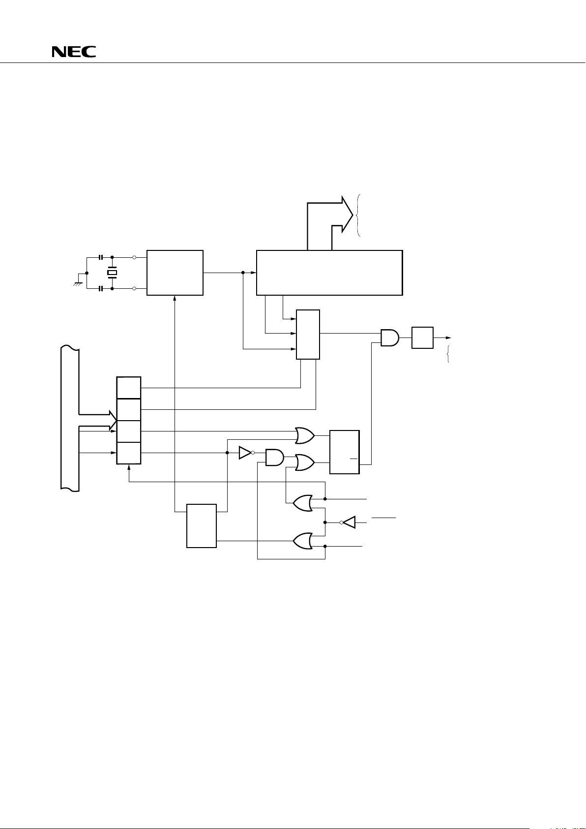
5.2 CLOCK GENERATOR
The clock generator operation is determined by the processor clock control register (PCC).
This circuit can also change the instruction execution time.
• 0.95
µ
s/1.91 µs/15.3 µs (4.19 MHz operation)
Fig. 5-1 Clock Generator Block Diagram
* Instruction execution
Remarks 1. fXX = Crystal/ceramic oscillator frequency
2. fX = External clock frequency
3.Φ = CPU Clock
4. PCC : Processor clock control register
5. One Φ clock cycle (tCY) is one machine cycle. See "AC
CHARACTERISTICS" in 12. "ELECTRICAL SPECIFICATIONS" for tCY.
★
X1
f
XX
or f
X
• Basic Interval Timer (BT)
• Clock Output Circuit
• Timer/Event Counter
• Serial Interface
Frequency Divider
1/2
Selector
HALT F/F
Wait Release Signal from BT
RESET Signal (Internal Reset)
Standby Release Signal from
Interrupt Control Circuit
STOP F/F
S
R
Q
PCC2,
PCC3
Clear
Oscillation
Stop
PCC
4
Internal Bus
System Clock
Oscillation
Circuit
S
R
Q
HALT *
STOP *
Frequency
Divider
1/4
• CPU
• Clock Output Circuit
Φ
1/16
X2
1/8 to 1/4096
PCC0
PCC1
PCC2
PCC3
20
µ
PD75116H,75117H
5.3 CLOCK OUTPUT CIRCUIT
The clock output circuit is a circuit which outputs a clock pulse from P22/PCL and is used to supply clock pulses
to remote control outputs or peripheral LSI’s.
• Clock output (PCL) :
Φ
, 524 kHz, 262 kHz (4.19 MHz operation)
Fig. 5-2 Configuration of Clock Output Circuit
CLOM3
CLOM1
CLOM0
4
Internal Bus
CLOM
P22
Output Latch
PORT2.2 Bit 2 of PMGB
Bit Specified
in Port 2
Input/Output
Mode
Output Buffer
PCL/P22
f
XX
/2
3
fXX/2
4
Selector
Φ
From Clock
Generator
CLOM2

21
µ
PD75116H,75117H
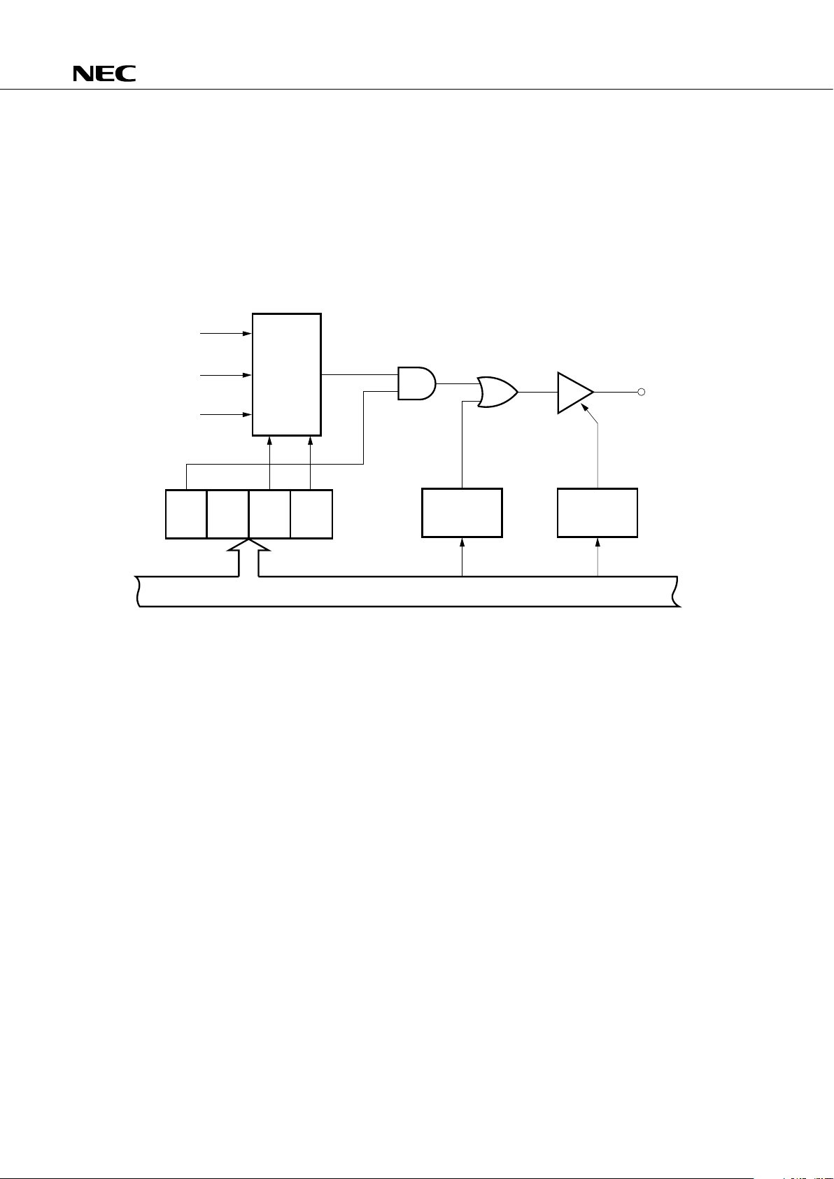
5.4 BASIC INTERVAL TIMER
The basic interval timer includes the following functions.
• It operates as an interval timer which generates reference time interrupts.
• It can be applied as a watchdog timer which detects when a program is out of control.
• Selects and counts wait times when the standby mode is released.
• It reads count contents.
Fig. 5-3 Basic Interval Timer Configuration
* SET1 indicates instruction execution.
5.5 TIMER/EVENT COUNTER
The
µ
PD75117H incorporates two internal timer/event counter channels.
Timer/event counter channel 0 and channel 1 differ only in selectable count pulse (CP) and clock supply function
to serial interface and are the same in other configurations and functions.
• Operates as a programmable interval timer.
• Outputs square waves in the desired frequency to the PTOn pin.
• Operates as an event counter.
• Use of TIn pin as an external interrupt input pin.
• Divides the TIn pin input into N divisions and outputs it to the PTOn pin (frequency divider operation).
• Supplies a serial shift clock to the serial interface circuit. (channel 0 only)
• Count status read function.
Internal Bus
f
XX
/2
5
fXX/2
7
fXX/2
12
From Clock
Generator
4
BTM3 BTM2 BTM1 BTM0 BTM
MPX
BT IRQBT
Set
BT Interrupt
Request Flag
Clear Clear
Basic Interval Timer
(8-Bit Frequency Divider)
Wait Release
Signal during
Standby Release
8
3
Vector
Interrupt
Request
Signal
f
XX
/2
9
SET1*

22
µ
PD75116H,75117H
Fig. 5-4 Timer/Event Counter Block Diagram (n = 0, 1)
* SET1 : Instruction execution.
From Clock
Generator
Input Buffer
MPX
TMn6
SET1
*1
TMn
Timer Operation Start
CP
Count Register (8)
Clear
8
Comparator (8)
8
8
Modulo Register (8)
8
8
Internal Bus
TMODn
Match
TOUT
F/F
TOEn
TO
Enable
Flag
P2n
Output
Latch
PORT2.n Bit 2 of PGMB
Port 2
Input/
Output
Mode
To Serial
Interface
(Channel 0 only)
P2n/PTOn
Output
Buffer
INTTn
IRQTn Set
Signal
IRQTn
Clear Signal
Tn
TIn
TIn
TMn7 TMn5 TMn4 TMn3 TMn2 TMn1 TMn0
TOn
TO
Selector
Edge
Detector
TMn0
RESET
TMn1
TOFn

23
µ
PD75116H,75117H
5.6 SERIAL INTERFACE
The serial interface has the following functions.
• Clock 8-bit transmission/reception operation (simultaneous transmission/reception)
• Clock 8-bit reception operation (SO output high impedance)
• Half-duplex asynchronous transfer (software control)
• LSB-first/MSB-first switchable
These functions facilitate serial bus data communications with other computers such as
µ
PD7500 series, 78K
series, etc., or conjunction with a peripheral device.

24
µ
PD75116H,75117H
* SET1 : instruction execution
Fig. 5-5 Serial Interface Block Diagram
Shift Registor (8)
Serial Clock
Counter (3)
Clear
Overflow
Serial Start
SIOM7 SIOM6 SIOM5 SIOM4 SIOM3 SIOM2 SIOM1 SIOM0
SIOM
SET1 *
88
8
P03/SI
P02/SO
P01/SCK
SIO7
SIO
SIO0
INTSIO
IRQSIO
Set Signal
IRQSIO
Clear Signal
TOF0
(from Timer Channel 0)
f
xx
/2
10
fxx/2
4
ϕ
MPX
R
SQ
Internal Bus

25
µ
PD75116H,75117H
5.7 PROGRAMMABLE THRESHOLD PORT (ANALOG INPUT PORT)
The µPD75117H is provided with 4-bit analog input pins (PTH00 to PTH03) for which the threshold voltage can
be changed. These pins have a configuration as shown in Fig. 5-6.
The threshold voltage (V
REF) can be selected in 16 ways (VDD × ——— – VDD × ———) and analog signals can be
directly input.
This port can also be used as a digital signal input port by selecting V
DD × ——— as VREF.
Fig. 5-6 Programmable Threshold Port Block Diagram
16
16
0.5
15.5
7.5
16
★
PTHM7
PTHM6
PTHM5
PTHM4
PTHM3
PTHM2
PTHM1
PTHM0
PTHM
4
MPX
V
REF
V
DD
PTH00
PTH01
PTH02
PTH03
+
–
+
–
+
–
+
–
Operation
Stopped
PTH0
Input Buffer
Programmable Threshold
Port Input Latch (4)
Internal Bus
8
2
1
R
2
1
R
R
R

26
µ
PD75116H,75117H
5.8 BIT SEQUENTIAL BUFFER ······ 16 BITS
Bit manipulation of the bit sequential buffer is the bit manipulation special data memory. Since, in particular,
the bit manipulation can easily be performed by changing sequentially address and bit specification, it is convenient
when processing data comprising a large number of bits bit-wise.
Fig. 5-7 Bit Sequential Buffer Format
Remarks In pmem. @L addressing, the specified bit moves according to the L register.
321032 1032103210
L = 0 L = 3 L = 4
DECS L
L = 7 L = 8
INCS L
L = B L = C L = F
FC3H FC2H FC1H FC0H
Symbol
Address
L Register
BSB3 BSB2 BSB1 BSB0
Bit

27
µ
PD75116H,75117H
6. INTERRUPT FUNCTION
The µPD75117H has 7 interrupt sources. Multiple interrupts with priority is are also possible.
Two test sources are also provided. The test sources are edge detection testable inputs.
Table 6-1 Interrupt Sources
INTBT (standard time interval signal from
basic interval timer)
INT4 (both rising edge and falling edge
detection)
INT0
INT1
INTT0 (match signal from timer/event
counter# 0 or TI0 input edge detection)
INTT1 (match signal from timer/event
counter# 1 or TI1 input edge detection)
INT2*2 (rising edge detection)
INT3*2 (rising edge detection)
Vector Interrupt Request
Signal
(Vector Table Address)
(rising edge and falling edge
detection selection)
Internal
External
1
2
Interrupt Order*1Internal/ExternalInterrupt Source
External
External
VRQ1
(0002H)
VRQ3
(0006H)
INTSIO (serial data transfer end signal)
Internal
Internal/external
Internal/external
3
4
5
VRQ4
(0008H)
VRQ5
(000AH)
VRQ2
(0004H)
External
Testable input signal
(Set IRQ2 and IRQ3)
*1.The interrupt order is the priority order when multiple interrupt requests are generated simultaneously.
2. INT2 and INT3 are of test sources . These are affected by interrupt enable flags in the same way as interrupt
sources, but do not generate vector interrupts.
The µPD75117H interrupt control circuit has the following functions:
• Hardware control vector interrupt function that can control interrupt acceptance by interrupt enable flag (IE×××)
and interrupt master enable flag (IME).
• Arbitrary setting of interrupt start address.
• Multiple interruption function by which priority can be specified using the interrupt priority selection register
(IPS).
• Interrupt request flag (IRQ×××) test function (interrupt generation confirmation by software possible).
• Standby mode release (selection of interrupt that releases the standby mode by interrupt enable flag possible).

28
µ
PD75116H,75117H
Fig. 6-1 Interrupt Control Circuit Block Diagram
22
IM1 IM0
IRQBT
INT4
/P00
INT0
/P10
INT1
/P11
INT2
/P12
IRQ4
IRQ0
IRQ1
IRQSIO
IRQT0
IRQT1
IRQ2
INT
BT
INTSIO
INTT0
INTT1
(IME) IST
Internal Bus
Vector
Table
Address
Generator
Priority Control
Circuit
Standby Release
Signal
Interrupt Enable Flag (IE
XXX
)
Edge
Detection
Circuit
Edge
Detection
Circuit
Decoder
IPS
42
INT3
/P13
Edge
Detection
Circuit
Edge
Detection
Circuit
Interrupt
Request
Flag
9
IRQ3
Edge
Detection
Circuit

29
µ
PD75116H,75117H
7. STANDBY FUNCTION
To reduce the power consumption during program wait, the µPD75117H has two standby modes (STOP mode
and HALT mode).
Table 7-1 Standby Mode Setting and Operation Status
Interrupt request signal from operable hardware enabled by interrupt enable flag, or
RESET input
STOP Mode
STOP instruction
System clock oscillation stopped
Operation possible only when the
external SCK input and TO0 output
(when timer/event counter 0 is external
TI0 input) are selected as a serial clock
Operable only when TIn pin input
specified as count clock
Operation stopped
Operation of INT0 to INT4 possible
Operation stopped
Setting instruction
Clock generator
Basic interval timer
Operation Status
HALT Mode
HALT instruction
Only CPU clock Φ stopped
Operable
(IRQBT set at reference time intervals)
Operation possible if a clock other than
Φ
is specified as a serial clock
Except CPU clock Φ, output possible.
Operation stopped
Serial interface
Timer/event counter
Clock output circuit
External interrupt
CPU
Operation possible
Release signal
Operation stopped

30
µ
PD75116H,75117H
8. RESET FUNCTION
The reset operation timing is shown in Fig. 8-1.
Fig. 8-1 Reset Operation by RESET Input
Wait
(31.3 ms/4.19 MHz)
HALT Mode Operating Mode
Internal Reset Operation
Operating Mode or Standby
Mode
RESET Input
The state of hardware after reset operation is as shown in Table 8-1.

31
µ
PD75116H,75117H
RESET Input in Standby
Mode
Table 8-1 Status of Each Hardware after Resetting (1/2)
RESET Input during
Operation
Low-order 6 bits of
program memory address
0000H are set in PC13 to PC8
and the contents of address
0001H are set in PC7 to PC0.
PC14*1 is set to 0.
Undefined
0
0
Sets program memory
address 000H bit 6 and bit
7 to RBE and MBE,
respectively.
Undefined
Undefined
Undefined
Undefined
0, 0
Low-order 6 bits of program
memory address 0000H are
set in PC13 to PC8 and the
contents of address 0001H
are set in PC7 to PC0. PC14*1
is set to 0.
Undefined
0
0
FFH
0
0, 0
Held
0
0
0
Held
0
0
Sets program memory
address 000H bit 6 and bit 7
to RBE and MBE, respectively.
Undefined
Undefined
Held *2
Held
0, 0
Basic interval
timer
Timer/event
counter
(n = 0, 1)
Serial interface
Clock generator,
clock output
circuit
Counter (BT)
Mode register (BTM)
Counter (Tn)
Modulo register (TMODn)
Mode register (TMn)
TOEn, TOFn
Shift register (SIO)
Mode register (SIOM)
Processor clock control register (PCC)
Clock output mode register (CLOM)
Undefined
0
0
FFH
0
0, 0
Undefined
0
0
0
Hardware
Program counter (PC)
Carry flag (CY)
Skip flag (SK0 to SK2)
PSW Interrupt status flag (IST0, IST1)
Bank enable flag (MBE, RBE)
Stack pointer (SP)
Stack bank selection register (SBS) *1
Data memory (RAM)
General register (X, A, H, L, D, E, B, C)
Bank selection register (MBS, RBS)
*1. Compatible with the µPD75117H only.
2. Data of data memory addresses 0F8H to 0FDH becomes undefined by RESET input.

32
µ
PD75116H,75117H
Table 8-1 Status of Each Hardware after Resetting (2/2)
RESET Input during
Operation
Hardware
RESET Input in Standby
Mode
Interrupt request
flag (IRQ×××)
Interrupt enable flag (IE×××)
Priority selection register (IPS)
INT0, INT1 mode registers (IM0, IM1)
Output buffer
Output latch
I/O mode register (PMGA, PMGB, PMGC)
PTH00 to PTH03 input latch
Mode register (PTHM)
Undefined
0
0
0
0, 0
Undefined
0
0
0
0, 0
Interrupt function
IRQ1,IRQ2, IRQ4
Other than above
OFF
Clear (0)
0
Undefined
0
0
Digital port
Analog port
Bit sequential buffer (BSB0 to BSB3)
OFF
Clear (0)
0
Undefined
0
0
★

33
µ
PD75116H,75117H
Identifier Description
reg X, A, B, C, D, E, H, L
reg1 X, B, C, D, E, H, L
rp XA, BC, DE, HL
rp1 BC, DE, HL
rp2 BC, DE
rp' XA, BC, DE, HL, XA', BC', DE', HL'
rp'1 BC, DE, HL, XA', BC', DE', HL'
rpa HL, HL+, HL–, DE, DL
rpa1 DE, DL
n4 4-bit immediate data or label
n8 8-bit immediate data or label
mem 8-bit immediate data or label*
bit 2-bit immediate data or label
fmem FB0H to FBFH, FF0H to FFFH immediate data or label
pmem FC0H to FFFH immediate data or label
µ
PD75116H 0000H to 3F7FH immediate data or label
µ
PD75117H 0000H to 3FFFH immediate data or label
addr1 0000H to 5F7FH immediate data or lebel
caddr 12-bit immediate data or label
faddr 11-bit immediate data or label
taddr 20H to 7FH immediate data (however, bit0 = 0) or label
PORTn PORT 0 to PORT 9, PORT12 to PORT14
IE××× IEBT, IESIO, IET0, IET1, IE0 to IE4
RBn RB0 to RB3
MBn MB0, MB1, MB2, MB15
9. INSTRUCTION SET
(1) Operand identifier and description
The operand is described in the operand field of each instruction in accordance with the description for the
operand identifier of the instruction. (For details, refer to RA75X Assembler Package User’s Manual Language
Volume (EEU-730).) When there are multiple elements in the description, one of the elements is selected. Upper
case letters and symbols (+,–) are keywords and are described unchanged.
Various register or flag symbols can be used as a label instead of mem, fmem, pmem, bit, etc. (For details, refer
to
µ
PD75117H User’s Manual (IEU-799).) However, there are restrictions on the labels for which fmem and pmem
can be used.
* In the case of the 8-bit data processing, an even address only can be described for mem.
addr

34
µ
PD75116H,75117H
(2) Operation description legend
A : A register; 4-bit accumulator
B : B register
C : C register
D : D register
E : E register
H : H register
L : L register
X : X register
XA : Register pair (XA); 8-bit accumulator
BC : Register pair (BC)
DE : Register pair (DE)
HL : Register pair (HL)
XA' : Extension register pair (XA')
BC' : Extension register pair (BC')
DE' : Extension register pair (DE')
HL' : Extension register pair (HL')
PC : Program counter
SP : Stack pointer
CY : Carry flag; bit accumulator
PSW : Program status word
MBE : Memory bank enable flag
RBE : Register bank enable flag
PORTn : Portn (n = 0 to 9, 12 to 14)
IME : Interrupt master enable flag
IPS : Interrupt priority selection register
IE××× : Interrupt enable flag
RBS : Register bank selection register
MBS : Memory bank selection register
PCC : Processor clock control register
. : Address, bit delimiter
(××) : Contents addressed by ××
××H : Hexadecimal data

35
µ
PD75116H,75117H
(3) Description of addressing area field symbols
*1
*2
*3
*4
*5
*6
*7
*8
*9
*10
*11
MB = MBE • MBS (MBS = 0, 1, 2, 15)
MB = 0
MBE = 0 : MB = 0 (00H to 7FH)
MB = 15 (80H to FFH)
MBE = 0 : MB = MBS (MBS = 0, 1, 2, 15)
MB = 15, fmem = FB0H to FBFH,
FF0H to FFFH
MB = 15, pmem = FC0H to FFFH
addr = 0000H to 3F7FH (µPD75116H)
0000H to 3FFFH (µPD75117H)
• µPD75116H
addr = (Current PC) –15 to (Current PC) –1,
(Current PC) + 2 to (Current PC) + 16
• µPD75117H
addr1 = (Current PC) –15 to (Current PC) –1,
(Current PC) + 2 to (Current PC) + 16
caddr = 0000H to 0FFFH (PC 13, 12 = 00B : µPD75116H)
= 0000H to 0FFFH (PC14, 13, 12 = 000B : µPD75117H)
= 1000H to 1FFFH (PC13, 12 = 01B : µPD75116H)
= 1000H to 1FFFH (PC14, 13, 12 = 001B : µPD75117H)
= 2000H to 2FFFH (PC13, 12 = 10B : µPD75116H)
= 2000H to 2FFFH (PC14, 13, 12 = 010B : µPD75117H)
= 3000H to 3F7FH (PC 13, 12 = 11B : µPD75116H)
= 3000H to 3FFFH (PC14, 13, 12 = 011B : µPD75117H)
= 4000H to 4FFFH (PC14, 13, 12 = 100B : µPD75117H)
= 5000H to 5F7FH (PC14, 13, 12 = 101B : µPD75117H)
faddr = 0000H to 07FFH
taddr = 0020H to 007FH
addr1 = 0000H to 5F7FH ( : µPD75117H only)
Data memory
addressing
→
Remarks 1. MB indicates the accessible memory bank.
2. For *2, MB = 0 without regard to MBE and MBS.
3. For *4 and *5, MB = 15 without regard to MBE and MBS.
4. *6 to *10 indicate the addressable area.
Program memory
addressing
→
→
→

36
µ
PD75116H,75117H
(4) Explanation of machine cycle field
S shows the number of machine cycles required when skip is performed by an instruction with skip. The value
of S changes as follows:
• No skip ....................................................................................................................................................................... S = 0
• When instruction to be skipped is 1-byte or 2-byte instruction......................................................................... S = 1
• When instruction to be skipped is 3-byte instruction.......................................................................................... S = 2
(BR !addr, BRA !addr1*, CALL !addr, CALLA !addr1* instructions)
* This instruction is valid for the
µ
PD75117H only.
Note One machine cycle is required to skip a GETI instruction.
One machine cycle is equivalent to one cycle (= tCY) of the CPU clockΦ. Three times can be selected by PCC setting.

37
µ
PD75116H,75117H
A, #n4
reg1, #n4
XA, #n8
HL, #n8
rp2, #n8
A, @HL
A, @HL+
A, @HL-
A, @rpa1
XA, @HL
@HL, A
@HL, XA
A, mem
XA, mem
mem, A
mem, XA
A, reg
XA, rp'
reg1, A
rp'1, XA
A, @HL
A, @HL+
A, @HL-
A, @rpa1
XA, @HL
A, mem
XA, mem
A,reg1
XA, rp'
XA, @PCDE
XA, @PCXA
XA, @BCDE*
XA, @BCXA*
1
2
2
2
2
1
1
1
1
2
1
2
2
2
2
2
2
2
2
2
1
1
1
1
2
2
2
1
2
1
1
1
1
A ← n4
reg1 ← n4
XA ← n8
HL ← n8
rp2 ← n8
A ← (HL)
A ← (HL), then L ← L + 1
A ← (HL), then L ← L – 1
A ← (rpa1)
XA ← (HL)
(HL) ← A
(HL) ← XA
A ← (mem)
XA ← (mem)
(mem) ← A
(mem) ← XA
A ← reg
XA ← rp'
reg1 ← A
rp'1 ← XA
A ↔ (HL)
A ↔ (HL), then L ← L + 1
A ↔ (HL), then L ← L – 1
A ↔ (rpa1)
XA ↔ (HL)
A ↔ (mem)
XA ↔ (mem)
A ↔ reg1
XA ↔ rp'
XA ← (PC13-8 + DE)ROM
XA ← (PC14-8 + DE)ROM
XA ← (PC13-8 + XA)ROM
XA ← (PC14-8 + XA)ROM
XA ← (B2-0 + CDE)ROM
XA ← (B2-0 + CXA)ROM
Skip
Condition
Stack A
Stack A
Stack B
L = 0
L = FH
L = 0
L = FH
*1
*1
*1
*2
*1
*1
*1
*3
*3
*3
*3
*1
*1
*1
*2
*1
*3
*3
*11
*11
Transfer
Table reference
Mnemonic Operands Bytes
Machine
Cycles
Operation
Instruction Group
Addressing
Area
XCH
MOV
MOVT
1
2
2
2
2
1
2 + S
2 + S
1
2
1
2
2
2
2
2
2
2
2
2
1
2 + S
2 + S
1
2
2
2
1
2
3
3
3
3
* The 3 lower bits in the B register are valid only.
Remarks Shading indicates a part compatible with the
µ
PD75117H.

38
µ
PD75116H,75117H
CY, fmem.bit
CY, pmem.@L
CY, @H+mem.bit
fmem.bit, CY
pmem.@L, CY
@H+mem.bit, CY
A, #n4
XA, #n8
A, @HL
XA, rp'
rp'1, XA
A, @HL
XA, rp'
rp'1, XA
A, @HL
XA, rp'
rp'1, XA
A, @HL
XA, rp'
rp'1, XA
A, #n4
A, @HL
XA, rp'
rp'1, XA
A, #n4
A, @HL
XA, rp'
rp'1, XA
A, #n4
A, @HL
XA, rp'
rp'1, XA
CY ← (fmem.bit)
CY ← (pmem7 – 2 + L3 – 2.bit(L1–0))
CY ← (H + mem3 – 0.bit)
(fmem.bit) ← CY
(pmem7 – 2 + L3 – 2.bit(L1–0)) ← CY
(H + mem3 – 0.bit) ← CY
A ← A + n4
XA ← XA + n8
A ← A + (HL)
XA ← XA + rp'
rp'1 ← rp'1 + XA
A, CY ← A + (HL) + CY
XA, CY ← XA + rp' + CY
rp'1, CY ← rp'1 + XA + CY
A ← A – (HL)
XA ← XA – rp'
rp'1, CY ← rp'1 – XA – CY
A, CY ← A – (HL) – CY
XA, CY ← XA – rp' – CY
rp'1, CY ← rp'1 – XA – CY
A ← A ∧ n4
A ← A ∧ (HL)
XA ← XA ∧ rp'
rp'1 ← rp'1 ∧ XA
A ← A ∨ n4
A ← A ∨ (HL)
XA ← XA ∨ rp'
rp'1 ← rp'1 ∨ XA
A ← A ∨ n4
A ← A ∨ (HL)
XA ← XA ∨ rp'
rp'1 ← rp'1 ∨ XA
Skip
Condition
Operands Bytes
Machine
Cycles
Operation
Addressing
Area
*4
*5
*1
*4
*5
*1
*1
*1
*1
*1
*1
*1
*1
carry
carry
carry
carry
carry
borrow
borrow
borrow
Instruction
Group
Mnemonic
MOV1
Bit
transfer
ADDS
2
2
2
2
2
2
1
2
1
2
2
1
2
2
1
2
2
1
2
2
2
1
2
2
2
1
2
2
2
1
2
2
ADDC
SUBC
AND
Operations
2
2
2
2
2
2
1 + S
2 + S
1 + S
2 + S
2 + S
1
2
2
1 + S
2 + S
2 + S
1
2
2
2
1
2
2
2
1
2
2
2
1
2
2
SUBS
OR
XOR

39
µ
PD75116H,75117H
A
A
reg
rp1
@HL
mem
reg
rp'
reg, #n4
@HL, #n4
A, @HL
XA, @HL
A, reg
XA, rp'
CY
CY
CY
CY
mem.bit
fmem.bit
pmem.@L
@H + mem.bit
mem.bit
fmem.bit
pmem.@L
@H + mem.bit
mem.bit
fmem.bit
pmem.@L
@H + mem.bit
mem.bit
fmem.bit
pmem.@L
@H + mem.bit
fmem.bit
pmem.@L
@H + mem.bit
Operands
Operation
Instruction
Group
Mne-
monic
Bytes
1
2
1
1
2
2
1
2
2
2
1
2
2
2
1
1
1
1
2
2
2
2
2
2
2
2
2
2
2
2
2
2
2
2
2
2
2
Machine
Cycles
CY ← A0, A3 ← CY, An–1 ← An
A ← A
reg ← reg + 1
rp1 ← rp1 + 1
(HL) ← (HL) + 1
(mem) ← (mem) + 1
reg ← reg – 1
rp' ←rp' – 1
Skip if reg = n4
Skip if (HL) = n4
Skip if A = (HL)
Skip if XA = (HL)
Skip if A = reg
Skip if XA = rp'
CY ← 1
CY ← 0
Skip if CY = 1
CY ← CY
(mem.bit) ← 1
(fmem.bit) ← 1
(pmem7–2 + L3–2.bit (L1–0)) ← 1
(H + mem3–0.bit) ← 1
(mem.bit) ← 0
(fmem.bit) ← 0
(pmem7–2 + L3–2.bit (L1–0)) ← 0
(H + mem3–0.bit) ← 0
Skip if (mem.bit) = 1
Skip if (fmem.bit) = 1
Skip if (pmem7–2 + L3–2.bit (L1–0)) = 1
Skip if (H + mem3–0.bit) = 1
Skip if (mem.bit) = 0
Skip if (fmem.bit) = 0
Skip if (pmem7–2 + L3–2.bit (L1–0)) = 0
Skip if (H + mem3–0.bit) = 0
Skip if (fmem.bit) = 1 and clear
Skip if (pmem7–2 + L3–2.bit (L1–0))
= 1 and clear
Skip if (H + mem3–0.bit)
= 1 and clear
Addressing
Area
Skip Condition
reg = 0
rp1 = 00H
(HL) = 0
(mem) = 0
reg = FH
rp' = FFH
reg = n4
(HL) = n4
A = (HL)
XA = (HL)
A = reg
XA = rp'
CY = 1
(mem.bit) = 1
(fmem.bit) = 1
(pmem.@L) = 1
(@H + mem.bit) = 1
(mem.bit) = 0
(fmem.bit) = 0
(pmem.@L) = 0
(@H + mem.bit) = 0
(fmem.bit) = 1
(pmem.@L) = 1
(@H + mem.bit) = 1
1
2
1 + S
1 + S
2 + S
2 + S
1 + S
2 + S
2 + S
2 + S
1 + S
2 + S
2 + S
2 + S
1
1
1 + S
1
2
2
2
2
2
2
2
2
2 + S
2 + S
2 + S
2 + S
2 + S
2 + S
2 + S
2 + S
2 + S
2 + S
2 + S
RORC
*1
*3
*1
*1
*1
*3
*4
*5
*1
*3
*4
*5
*1
*3
*4
*5
*1
*3
*4
*5
*1
*4
*5
*1
SKE
Comparison
SET1
CLR1
SKT
NOT1
Carry flag
manipulation
SET1
Memory bit
manipulation
CLR1
SKT
SKF
SKTCLR
Accumulator
manipulation
NOT
INCS
Increment
/decrement
DECS

40
µ
PD75116H,75117H
Instruction
Group
Mne-
monic
Branch
Bytes
Machine
Cycles
Addressing
Area
Skip
Condition
Operation
Operands
*4
*5
*1
*4
*5
*1
*4
*5
*1
*6
*11
*6
*7
*11
*11
*11
*8
*6
AND1
Memory bit
manipulation
XOR1
2
2
2
2
2
2
2
2
2
—
—
3
2
2
3
3
3
3
3
2
3
4
OR1
2
2
2
2
2
2
2
2
2
—
—
3
1
1
2
2
2
2
3
2
3
BR
BRCB
BRA
Subroutine
stack
control
CALL
CY, fmem.bit
CY, pmem.@L
CY, @H + mem.bit
CY, fmem.bit
CY, pmem.@L
CY, @H + mem.bit
CY, fmem.bit
CY, pmem.@L
CY, @H + mem.bit
addr *1
addr1
!addr
$addr
$addr1
PCDE
PCXA
BCDE *2
BCXA *2
!addr1
!caddr
!addr
*1.µPD75116H only.
2. The 3 lower bits in the B register are valid only.
Remarks Shading indicates a part compatible with the
µ
PD75117H.
CY ← CY ∧ (fmem.bit)
CY ← CY ∧ (pmem7–2 + L3–2.bit (L1–0))
CY ← CY ∧ (H + mem3–0.bit)
CY ← CY ∨ (fmem.bit)
CY ← CY ∨ (pmem7–2 + L3–2.bit (L1–0))
CY ← CY ∨ (H + mem3–0.bit)
CY ← CY ∨ (fmem.bit)
CY ← CY ∨ (pmem7–2 + L3–2.bit (L1–0))
CY ← CY ∨ (H + mem3–0.bit)
PC13–0 ← addr
(The assembler selects the optimum instruction from among the BR !addr, BRCB
!caddr, and BR $addr instructions.)
PC14–0 ← addr1
(The assembler selects the optimum instruction from among the BR !addr, BRA
!addr1, BRCB !caddr, and BR $addr1 instructions.)
PC13-0 ← addr
PC14-0, PC13-0 ← addr
PC13-0 ← addr
PC14-0 ← addr1
PC13-0 ← PC13-8 + DE
PC14-0 ← PC14-8 + DE
PC13-0 ← PC13-8 + XA
PC14-0 ← PC14-8 + XA
PC14-0 ← B2-0 + CDE
PC14-0 ← B2-0 + CXA
PC14-0 ← !addr1
PC13-0 ← PC13,12 + caddr11-0
PC14-0 ← PC14,13,12 + caddr11-0
(SP – 4) (SP – 1) (SP – 2) ← PC11-0
(SP – 3) ← MBE, RBE, PC13, PC12
PC13-0 ← addr, SP ← SP–4
(SP – 2) ← ×, ×, MBE, RBE
(SP – 6) (SP – 3) (SP – 4) ← PC11-0
(SP – 5) ← 0, PC14, PC13, PC12
PC14 ← 0, PC13-0 ← addr, SP ← SP–6

41
µ
PD75116H,75117H
(SP – 2) ← ×, ×, MBE, RBE
(SP – 6) (SP – 3) (SP – 4) ← PC11-0
(SP – 5) ← 0, PC14, PC13, PC12
PC14–0 ← addr1, SP ← SP–6
(SP – 4) (SP – 1) (SP – 2) ← PC11–0
(SP – 3) ← MBE, RBE, PC13, PC12
PC13–0 ← 000 + faddr, SP ← SP – 4
(SP – 2) ← ×, ×, MBE, RBE
(SP – 6) (SP – 3) (SP – 4) ← PC11–0
(SP – 5) ← 0, PC14, PC13, PC12
PC14–0 ← 0000 + faddr, SP ← SP – 6
MBE, RBE, PC13, PC12 ← (SP + 1)
PC11–0 ← (SP) (SP + 3) (SP + 2)
SP ← SP + 4
PC11–0 ← (SP) (SP + 3) (SP + 2)
×, PC14, PC13, PC12 ← (SP + 1)
×, ×, MBE, RBE ← (SP + 4)
SP ← SP +6
MBE, RBE, PC13, PC12 ← (SP + 1)
PC11–0 ← (SP) (SP + 3) (SP + 2)
SP ← SP + 4, then skip unconditionally
PC11–0 ← (SP) (SP + 3) (SP + 2)
×, PC14, PC13, PC12 ← (SP + 1)
×, ×, MBE, RBE ← (SP + 4)
SP ← SP +6 then skip unconditionally
PC13, PC12 ← (SP + 1)
PC11–0 ← (SP) (SP + 3) (SP + 2)
PSW ← (SP + 4) (SP + 5), SP ← SP +6
PC11–0 ← (SP) (SP + 3) (SP + 2)
×, PC14, PC13, PC12 ← (SP + 1)
PSW ← (SP + 4) (SP + 5), SP ← SP +6
(SP – 1) (SP – 2) ← rp, SP ← SP – 2
(SP – 1) ← MBS, (SP – 2) ← RBS, SP ← SP – 2
rp ← (SP + 1) (SP), SP ← SP + 2
MBS ← (SP + 1), RBS ← (SP), SP ← SP + 2
IME (IPS.3) ← 1
IE××× ← 1
IME (IPS.3) ← 0
IE××× ← 0
Operation
Instruction
Group
Mne-
monic
Skip Condition
Operands Bytes
Machine
Cycles
Addressing
Area
Subroutine
stack
control
PUSH
POP
EI
DI
rp
BS
rp
BS
IE×××
IE×××
1
2
1
2
2
2
2
2
1
2
1
2
2
2
2
2
Interrupt
control
CALLA !addr1
3
3
*11
*9
CALLF
!faddr
2
2
3
1
RET
Unconditional
3 + S
1
RETS
3
1
RETI
Remarks Shading indicates a part compatible with the µPD75117H.
3

42
µ
PD75116H,75117H
Operation
Instruction
Group
Mne-
monic
Skip Condition
Operands
Addressing
Area
------------------------
Bytes
Machine
Cycles
2
2
2
2
2
2
1
2
2
2
2
2
2
2
2
1
2
2
A← PORTn (n = 0 to 9, 12 to 14)
XA ← PORTn + 1, PORTn (n = 4, 6, 8, 12)
PORTn ← A (n = 2 to 9, 12 to 14)
PORTn + 1, PORTn ← XA (n = 4, 6, 8, 12)
Set HALT Mode (PCC.2 ← 1)
Set STOP Mode (PCC.3 ← 1)
No Operation
RBS ← n (n = 0 to 3)
MBS ← n (n = 0, 1, 2, 15)
• TBR Instruction
PC13–0 ← (taddr)5–0 ← (taddr + 1)
PC14← 0
• TCALL Instruction
(SP – 5) (SP – 6) (SP – 3)(SP – 4) ← PC14–0
(SP – 2) ← (×, ×, MBE, RBE)
PC13–0 ← (taddr)5–0 ← (taddr + 1)
SP ← SP – 6 PC14← 0
• Other than TBR and TCALL Instruction
Execution of an instruction addressed
at (taddr) and (taddr + 1)
• TBR Instruction
PC13–0 ← (taddr)5–0 ← (taddr + 1)
PC14← 0
• TCALL Instruction
(SP – 5) (SP – 6) (SP – 3)(SP – 4) ← ×, PC14–0
(SP – 2) ← ×, ×, MBE, RBE
PC13–0 ← (taddr)5–0 ← (taddr + 1)
SP ← SP – 6, PC14← 0
• Other than TBR and TCALL Instruction
Execution of an instruction addressed
at (taddr) and (taddr + 1)
A, PORTn
XA, PORTn
PORTn, A
PORTn, XA
RBn
MBn
*1
HALT
STOP
NOP
IN
*1
OUT
Input/output
CPU control
SELL
taddr
*2
GETI
Special
-----------------------
Conforms to
referenced
instruction.
Conforms to
referenced
instruction.
------------------------
------------------------------------------------------------------------
------------------------------------------------------------------------
3
3
4
*10
1
*10
1
------------------------
------------------------------------------------------------------------
------------------------------------------------------------------------
4
3
3
Remarks Shading indicates a part compatible with the µPD75117H.
*1.When executing the IN/OUT instruction, <MBE = 0> or <MBE = 1, MBS = 15> must be set.
2. The TBR or TCALL instruction is a GETI instruction table definition assembler pseudo-instruction.

43
µ
PD75116H,75117H
10. APPLICATION EXAMPLE
10.1 CORDLESS TELEPHONE (SUBSET)
Legend
IDC : Immediate Deviation Controller, ID ROM : ID (Identification) Code ROM, LCD : Liquid Crystal Display
LED : Light Emitting Diode, MPX : Multiplexer MSK : Minimum Shift Keying
PLL : Phase Locked Loop, SIO : Serial Data Input/Output TCXO : Temperature Compensation Crystal Oscillator
VCO : Voltage Control Oscillator
Power Amp
IDC
Amp
Compres-
sion
Transmitter/
Receiver
Extension
MPX
MSK
Modem
Speaker
Speaker
Amp
LED Display
Key Matrix
LED
Display
LCD
Controller/
Driver
Console
Detection
ID ROM
SIO
Radio Wave
Detection
Extra-Area
Detection
TCXO
PLL
VCO
Prescaler
PLL
VCO
Prescaler
MPX
Mixer
2SC4226
3SK177
Filter Amp
2SC2757
2SC4182
PD6252
PD7228
PD7511H
µ
µ
µ

44
µ
PD75116H,75117H
10.2 DISPLAY PAGER
Filter
INT
TO
Code ROM
Piezoelectric
Buzzer
Comparator
Input
High-Current
Output
LED Display
Switch
RAM
Battery Check
LCD Display
LCD Controller/Driver
SIO
PD75117H
PD7228/7229
µ
µ

45
µ
PD75116H,75117H
11. MASK OPTION SELECTION
The µPD75117H has the following mask option.
Pin Function
Mask Option
• Pull-up resistor (can be specified bit-wise.)
• No pull-up resistor (can be specified bit-wise.)
P12 to P14

46
µ
PD75116H,75117H
Supply voltage –0.3 to +7.0 V
VI1
VI2*1
VO
IOH
IOL*2
Topt
Tstg
VDD
–40 to +60 °C
–65 to +150 °C
Output current
high
12. ELECTRICAL SPECIFICATIONS
ABSOLUTE MAXIMUM RATINGS (Ta = 25 °C)
PARAMETER SYMBOL TEST CONDITIONS RATING UNIT
Except ports 12, 13 and 14 –0.3 to VDD +0.3 V
Input voltage Internal pull-up resistor –0.3 to VDD +0.3 V
Ports 12 to 14
Open–drain –0.3 to +7.3 V
Output voltage –0.3 to VDD +0.3 V
One pin –15 mA
All pins –30 mA
Peak value 30 mA
One pin
Effective value 15 mA
Peak value 100 mA
Output current low
Effective value 60 mA
Peak value 100 mA
Total of ports 3 to 9
Effective value 60 mA
Operating
temperature
Storage
temperature
*1.When a voltage exceeding 6V is applied to ports 12, 13 and 14, the power supply impedance (pull-up resistor)
should be 50KΩ or more.
2. Effective value should be calculated: [Effective value] = [Peak value] × √duty
Note Product quality may suffer if the absolute maximum rating is exceeded for even a single parameter or even
momentarily.
The absolute maximum ratings are rated values at which the product is on the verge of suffering physical
damage, and therefore the product must be used under conditions which ensure that the absolute
maximum ratings are not exceeded.
OPERATING VOLTAGE RANGE
CPU
Programmable threshold port
(comparator input)
Other hardware
– 40 + 60 °C
– 10 + 60 °C
– 40 + 60 °C
PARAMETER TEST CONDITIONS MIN. MAX. UNIT
★
Total of ports 0, 2, 12 to 14

47
µ
PD75116H,75117H
CAPACITANCE (Ta = 25 °C, VDD = 0 V)
PARAMETER SYMBOL TEST CONDITIONS MIN. TYP. MAX. UNIT
CIN
COUT
15 pF
15 pF
Input capacitance
Output capacitance
Input/output
capacitance
CIO
f = 1 MHz
Unmeasured pins returned to 0 V
15 pF
OSCILLATION CIRCUIT CHARACTERISTICS (Ta = –40 to +60 °C, VDD = 1.8 to 5.5 V)
RECOMMENDED TEST
RESONATOR PARAMETER MIN. TYP. MAX. UNIT
CONSTANT CONDITIONS
Ceramic
resonator
After VDD reaches
MIN. of oscillation
voltage range
Crystal
resonator
External
clock
2.0 5.0 *4 MHz
4ms
2.0 4.19 5.0 *4 MHz
10 ms
30 ms
2.0 5.0 *4 MHz
100 250 ns
Oscillator
frequency (fXX)
Oscillation
stabilization time
Oscillator
frequency (fXX)
Oscillation
stabilization time
X1 input
frequency (fX)
X1 input
high-/low-level width
(tXH, tXL)
X1 X2
µ
PD74HCU04
X1 X2
C1 C2
X1 X2
C1 C2
*5
*1
*1
*2
VDD = 4.5 to 5.5 V
VDD = 2.7 to 5.5 V
*2
*2
*3
*3
*1.When using in VDD < 2.7 V, the X2 pin oscillation waveform duty should be set within the range between 40%
and 60%.
t
XXL
t
XXH
V
SS
X2 Oscillation
Waveform
V
DD
1
2
V
DD
Duty =
t
XXL
(or t
XXH
)
t
XXL
+ t
XXH
× 100
2. Oscillator frequency and X1 input frequency indicate oscillation circuit characteristics only. See AC
CHARACTERISTICS for instruction execution time.
3. The oscillation stabilization time is the time required for oscillation to stabilize after V
DD reaches MIN. of
oscillation voltage range or the STOP mode is released.
4. When the oscillator frequency is 4.19 MHz < f
XX ≤ 5.0 MHz, PCC = 0011 should not be selected as the instruction
execution time. If PCC = 0011 is selected, one machine cycle is less than 0.95
µ
s and the rated MIN. value
of 0.95
µ
s is not observed.
5. The external clock cannot be used in V
DD < 2.7 V.

48
µ
PD75116H,75117H
Note When the clock oscillator is used, the following should be noted concerning wiring in the area in the figure
enclosed by a dotted line to prevent the influence of wiring capacitance, etc.
• The wiring should be kept as short as possible.
• No other signal lines should be crossed.
• Keep away from lines carrying a high fluctuating current.
• The oscillator capacitor grounding point should always be at the same potential as V
SS. Do not connect
to a ground pattern carrying a high current.
• A signal should be not taken from the oscillator.
RECOMMENDED OSCILLATION CIRCUIT CONSTANT
RECOMMENDED CERAMIC RESONATOR (Ta = –40 to +60 °C)
EXTERNAL CAPACITANCE (pF)
OSCILLATION VOLTAGE RANGE [V]
MANUFAC-
TURER
FREQUENCY
(MHz)
2.00
4.00
4.19
5.00
PRODUCT NAME
KBR–2.0MS
PBRC 2.00A
KBR–4.0MSA
PBRC 4.00A
KBR–4.0MKS
KBR–4.0MWS
KBR–4.19MSA
PBRC 4.19A
KBR–4.19MKS
KBR–4.19MWS
KBR–5.0MSA
PBRC 5.00A
KBR–5.0MKS
KBR–5.0MWS
MIN.
MAX.
C1
47
33
Iincorporated
33
Iincorporated
33
Iincorporated
C2
47
33
Iincorporated
33
Iincorporated
33
Iincorporated
1.8
5.5
Kyocera

49
µ
PD75116H,75117H
0.7 VDD VDD V
0.8 VDD VDD V
0.8 VDD VDD V
0.7 VDD VDD V
0.8 VDD VDD V
0.7 VDD 6V
0.8 VDD 6V
VDD – 0.5 VDD V
VDD – 0.3 VDD V
0 0.3 VDD V
0 0.2 VDD V
0 0.2 VDD V
0 0.4 V
0 0.25 V
VDD – 1.0 V
VDD – 0.8 V
VDD – 0.5 V
VDD – 0.2 V
0.35 2.0 V
0.4 V
0.5 V
0.3 V
0.35 2.0 V
0.3 1.0 V
0.4 V
0.5 V
0.3 V
0.35 2.0 V
0.4 V
0.5 V
0.3 V
3
µ
A
20
µ
A
15
µ
A
–3
µ
A
–20
µ
A
3
µ
A
15
µ
A
–3
µ
A
10 35 60 kΩ
PARAMETER SYMBOL TEST CONDITIONS MIN. TYP. MAX. UNIT
DC CHARACTERISTICS (Ta = –40 to +60 °C, VDD = 1.8 to 5.5 V)
Internal pull-up
resistor
(mask option)
Output leakage
current low
Output leakage
current high
RL
ILOL
ILOH2
ILOH1
ILIL2
ILIL1
Input leakage
current low
ILIH3
ILIH2
ILIH1 Other than below
X1, X2
Ports 12 to 14 (open-drain)
Other than below
X1, X2
Other than below
Ports 12 to 14 (open-drain)
VIN = VDD
VIV = 6 V
VIN = 0 V
VOUT = VDD
VOUT = 6 V
VOUT = 0 V
Ports 12 to 14
VOL
VDD = 2.7 to 5.5 V
VDD = 1.8 to 2.7 V
VDD = 4.5 to 5.5 V
VDD = 2.7 to 5.5 V
VDD = 2.7 to 5.5 V
VDD = 1.8 to 2.7 V
IOH = –1 mA
IOH = –100 µA
VOH
Input leakage
current high
Output voltage low
X1, X2
VIL3
Ports 0,1,TI0, 1, RESET
Other than below
VIL1
VDD = 2.7 to 5.5 V
VDD = 1.8 to 2.7 V
VDD = 2.7 to 5.5 V
VDD = 1.8 to 5.5 V
VDD = 2.7 to 5.5 V
VDD = 1.8 to 2.7 V
VDD = 2.7 to 5.5 V
VDD = 1.8 to 5.5 V
Ports
12 to 14
VIH4
X1, X2
VIH3
N-ch open–
drain
Internal pull-up
resistor
Ports 0,1,TI0, 1, RESET
VIH2
VIH1
Other than below
VDD = 2.7 to 5.5 V
VDD = 1.8 to 2.7 V
IOL = 15 mA
IOL = 1.6 mA
IOL = 400 µA
IOL = 100 µA
IOL = 15 mA
IOL = 10 mA
IOL = 1.6 mA
IOL = 400 µA
IOL = 100 µA
IOL = 10 mA
IOL = 1.6 mA
IOL = 400 µA
IOL = 100 µA
VDD = 4.5 to 5.5 V
VDD = 2.7 to 5.5 V
VDD = 2.7 to 5.5 V
VDD = 1.8 to 5.5 V
VDD = 4.5 to 5.5 V
VDD = 2.7 to 5.5 V
VDD = 2.7 to 5.5 V
VDD = 2.7 to 5.5 V
VDD = 1.8 to 5.5 V
VDD = 4.5 to 5.5 V
VDD = 2.7 to 5.5 V
VDD = 2.7 to 5.5 V
VDD = 1.8 to 5.5 V
Ports 12 to
14
Ports 3, 9
Ports 0, 2,
4 to 8
Output voltage high
VIL2Input voltage low
Input voltage high

50
µ
PD75116H,75117H
DC CHARACTERISTICS (Ta = –40 to +60 °C, VDD = 1.8 to 5.5 V)
VDD = 5 V ±10 % *2
VDD = 3 V ±10 % *2
VDD = 2 V ±10 % *3
VDD = 5 V ±10 %
VDD = 3 V ±10 %
VDD = 2 V ±10 %
VDD = 5 V ±10 %
STOP mode VDD = 3 V ±10 %
VDD = 2 V ±10 %
PARAMETER SYMBOL TEST CONDITIONS MIN. TYP. MAX. UNIT
3.0 9.0 mA
1.6 4.8 mA
0.6 1.8 mA
0.7 2.1 mA
280 860
µ
A
120 360
µ
A
0.2 50
µ
A
0.1 20
µ
A
0.05 10
µ
A
HALT
mode
*1.Excluding current flowing in the internal pull-up resistors and comparator circuit.
2. When the processor clock control register (PCC) is set to 0011 for operation in the high-speed mode.
3. When the PCC register is set to 0010 for operation in the low-speed mode.
COMPARATOR CHARACTERISTICS (Ta = –10 to +60 °C*, VDD = 1.8 to 5.5 V)
PARAMETER SYMBOL TEST CONDITIONS MIN. TYP. MAX. UNIT
VACOMP
VTH
VIPTH
Compare accuracy
Threshold voltage
PTH input voltage
Comparator circuit
current consumption
PTHM7 set to "1"
* The comparator cannot operate in the range of Ta = –40 to –10 °C. It must be used within the range of Ta =
–10 to +60 °C.
VDD = 5.0 V
VDD = 3.0 V
VDD = 2.0 V
±100 mV
0VDD V
0VDD V
0.7 mA
0.3 mA
0.1 mA
Supply current*1
4.19 MHz
Crystal oscillation
C1 = C2 = 22 pF
IDD1
IDD2
IDD3

51
µ
PD75116H,75117H
0.95 16
µ
s
1.91 16
µ
s
0 1 MHz
0 275 kHz
0.48
µ
s
1.8
µ
s
0.8
µ
s
0.95
µ
s
3.2
µ
s
3.8
µ
s
0.4
µ
s
tKCY/2 – 50
ns
1.6
µ
s
tKCY/2 – 150
ns
0 300 ns
0 1000 ns
VDD = 2.7 to 5.5 V
VDD = 2.7 to 5.5 V
VDD = 2.7 to 5.5 V
Input
VDD = 4.5 to 5.5 V
Output
Input
Output
Input
VDD = 4.5 to 5.5 V
Output
Input
Output
VDD = 4.5 to 5.5 V
AC CHARACTERISTICS (Ta = –40 to +60 °C, VDD = 1.8 to 5.5 V)
PARAMETER SYMBOL TEST CONDITIONS MIN. TYP. MAX. UNIT
fTI
tTIH,
tTIL
tCY
tKSI
tSIK
tKSO
100 ns
400 ns
TI0, TI1 input
frequency
TI0, TI1 input high/
low-level width
tKCY
SCK cycle time
SCK high/low-level
width
tKH,
tKL
SI setup time
(to SCK↑)
SI hold time
(from SCK↑)
SO output delay
time from SCK↓
INT0 to INT4
high/low-level width
RESET low-level
width
tINTH,
tINTL
tRSL
5
µ
s
5
µ
s
CPU clock cycle time*
(Minimum instruction
execution time = 1
machine cycle)

52
µ
PD75116H,75117H
* The CPU clock (Φ) cycle time is determined by the
oscillator frequency of the connected resonator
and the setting of the processor clock control
register (PCC). The graph on the right shows the
characteristic for cycle time t
CY supply current VDD
during system clock operation.
tCY vs. V
DD
Supply Voltage VDD [V]
012
3456
7
100
10
1.0
0.1
Cycle Time t
CY
[ s]
µ
Operating
Guarantee
Range
AC Timing Test Point (Except ports 0, 1, TI0, TI1, X1, X2, RESET)
(1) V
DD = 2.7 to 5.5 V
0.7 V
DD
0.3 V
DD
0.7 V
DD
0.3 V
DD
Test Points
(2) VDD = 1.8 to 2.7 V
0.8 V
DD
0.2 V
DD
0.8 V
DD
0.2 V
DD
Test Points

53
µ
PD75116H,75117H
Clock Timing
(1) V
DD = 2.7 to 5.5 V
X1 Input
1/f
X
t
XL
t
XH
VDD – 0.5 V
0.4 V
(2) VDD = 1.8 to 2.7 V
X1 Input
1/f
X
t
XL
t
XH
VDD – 0.3 V
0.25 V
TI0,TI1 Input Timing
TI0, TI1
1/f
TI
t
TIL
t
TIH
0.8 V
DD
0.2 V
DD

54
µ
PD75116H,75117H
SCK
Input Data
Output Data
t
KSO
SI
SO
0.8 V
DD
0.2 V
DD
0.8 V
DD
0.2 V
DD
t
KCY
t
KH
t
KL
t
SIK
t
KSI
Serial Transfer Timing
Interrupt Input Timing
RESET Input Timing
t
INTL
t
INTH
INT0–INT4
0.8 V
DD
0.2 V
DD
t
RSL
RESET
0.2 V
DD

55
µ
PD75116H,75117H
DATA MEMORY STOP MODE LOW SUPPLY VOLTAGE DATA RETENTION CHARACTERISTICS (Ta = –40 to +60 °C)
PARAMETER SYMBOL TEST CONDITIONS MIN. TYP. MAX. UNIT
Data retention supply voltage VDDDR 1.8 5.5 V
Data retention supply current*1 IDDDR VDDDR = 2.0 V 0.05 10
µ
A
Release signal set time tSREL 0
µ
s
Release by RESET 217/fXX ms
tWAIT
Release by interrupt request *3 ms
*1.Excluding current flowing in the internal pull-up resistors and comparator circuit.
2. The oscillation stabilization wait time is the time during which CPU operation is stopped to prevent unstable
operation when oscillation is started.
3. Depends on the basic interval timer mode register (BTM) setting (see table below).
WAIT TIME
BTM3 BTM2 BTM1 BTM0
(Figures in parentheses are for operation at fXX = 4.19 MHz)
—0 00 2
20
/fXX (approx. 250 ms)
—0 11 2
17
/fXX (approx. 31.3 ms)
—1 01 2
15
/fXX (approx. 7.82 ms)
—1 11 2
13
/fXX (approx. 1.95 ms)
STOP Mode
Data Retention Mode
STOP Instruction Execution
RESET
V
DD
Internal Reset Operation
HALT Mode
Operating
Mode
V
DDDR
t
SREL
t
WAIT
Data Retention Timing (STOP mode release by RESET)
Oscillation stabilization wait
time*2

56
µ
PD75116H,75117H
STOP Mode
Data Retention Mode
STOP Instruction Execution
V
DD
HALT Mode
Operating
Mode
V
DDDR
t
SREL
t
WAIT
Standby Release Signal
(Interrupt Request)
Data Retention Timing (Standby release signal: STOP mode release by interrupt signal)

57
µ
PD75116H,75117H
N
A
M
F
B
48
49
32
K
L
64 PIN PLASTIC QFP ( 14)
64
1
17
16
33
D
C
detail of lead end
S
Q
5°±5°
P
M
I
H
J
G
P64GC-80-AB8-3
ITEM MILLIMETERS INCHES
A
B
C
D
F
G
H
I
J
K
L
17.6±0.4
14.0±0.2
1.0
0.35±0.10
0.15
14.0±0.2
0.693±0.016
0.039
0.039
0.006
0.031 (T.P.)
0.551
NOTE
M
N
0.10
0.15
1.8±0.2
0.8 (T.P.)
0.004
0.006
+0.004
–0.003
Each lead centerline is located within 0.15
mm (0.006 inch) of its true position (T.P.) at
maximum material condition.
0.071±0.008
0.014
0.551
0.8±0.2
0.031
P 2.55 0.100
0.693±0.016
17.6±0.4
1.0
+0.009
–0.008
Q
0.1±0.1
0.004±0.004
S 2.85 MAX. 0.112 MAX.
+0.10
–0.05
+0.009
–0.008
+0.004
–0.005
+0.009
–0.008
13. PACKAGE INFORMATION
64-PIN PLASTIC QFP ( 14)

58
µ
PD75116H,75117H
64-PIN PLASTIC QFP ( 12)
★
K
J
N
A
M
F
B
48
49
32
L
64 PIN PLASTIC QFP ( 12)
64
1
17
16
33
G
detail of lead end
S
Q
5°±5°
H
D
C
P
M
I
P64GK-65-8A8
ITEM MILLIMETERS INCHES
A
B
C
D
F
G
H
I
J
K
L
14.8±0.4
12.0±0.2
1.125
0.30±0.10
0.13
12.0±0.2
0.583±0.016
0.044
0.044
0.005
0.026 (T.P.)
0.472
NOTE
M
N
0.10
0.15
1.4±0.2
0.65 (T.P.)
0.004
0.006
+0.004
–0.003
Each lead centerline is located within 0.13
mm (0.005 inch) of its true position (T.P.) at
maximum material condition.
0.055±0.008
0.012
0.472
0.6±0.2
0.024
P 1.4 0.055
0.583±0.016
14.8±0.4
1.125
+0.008
–0.009
Q
0.1±0.1
0.004±0.004
S 1.7 MAX. 0.067 MAX.
+0.10
–0.05
+0.009
–0.008
+0.004
–0.005
+0.009
–0.008

59
µ
PD75116H,75117H
14. RECOMMENDED SOLDERING CONDITIONS
The µPD75117H should be soldered and mounted under the conditions recommended in the table below.
For details of recommended conditions, refer to the information document "Semiconductor Device Mount
Technology Manual" (IEI-1207).
For soldering methods and conditions other than those recommended below, contact our sales personnel.
Table 14-1 Surface Mount Type Soldering Conditions
(1)
µ
PD75117HGC: 64-Pin Plastic QFP ( 14 mm)
★
Recommended
Condition Symbol
Soldering Method Soldering Conditions
Package peak temperature : 230 °C, Duration : 30 sec. max. (at 210 °C or
avove), Number of times : twice
<Points to note>
Flux washing by the water after the first reflow should be avoided.
Package peak temperature : 215 °C, Duration : 40 sec. max. (at 200 °C or
above), Number of times : twice
<Points to note>
Flux washing by the water after the first reflow should be avoided.
Solder bath temperature : 260 °C max., Duration : 10 sec. max., Number of
times : once, Preheating temperature : 120 °C max. (package surface
temperature)
Pin part temperature : 300 °C max., Duration : 3 sec. max. (per device side)
Pin part heating
Wave soldering
WX60-00-1
VP15-00-2
VPS
Infrared reflow
(2)µPD75117GK: 64-Pin Plastic QFP ( 12 mm)
Recommended
Condition Symbol
Soldering Method Soldering Conditions
Package peak temperature : 230 °C, Duration : 30 sec. max. (at 210 °C or
avove), Number of times : twice, Time limit: 7 days* (thereafter 10 hours
prebaking at 125 ˚C required)
<Points to note>
Flux washing by the water after the first reflow should be avoided.
Package peak temperature : 215 °C, Duration : 40 sec. max. (at 200 °C or
above), Number of times : twice, Time limit: 7 days* (thereafter 10 hours
prebaking at 125 ˚C required)
<Points to note>
Flux washing by the water after the first reflow should be avoided.
Pin part temperature : 300 °C max., Duration : 3 sec. max. (per device side)
IR30-00-2
Infrared reflow
Pin part heating
—
—
VP15-107-2
IR35-107-2
VPS
* For the storage period after dry-pack decupsulation storage conditions are max. 25 ˚C, 65 % RH.
Note Use of more than one soldering method should be avoided (except in the case of pin part heating).

60
µ
PD75116H,75117H
Item
4K/6K/8K/12K/16K 4K/8K 8K/12K/16K
(Mask ROM) (Mask ROM) (Mask ROM)
320/320/512/512/512 320/512 512
ROM (byte)
RAM (× 4 bits)
µ
PD75104/106/108/112/116
µ
PD75104A/108A
µ
PD75108F/112F/116F
Product Name
APPENDIX A. FUNCTIONAL DIFFERENCES AMONG µPD751×× SERIES PRODUCTS
10 (Pull-up resistor mask option : 4)
32 (Pull-up resistor mask option : 24,
LED direct drive capability)
10
10
Withstand voltage
CMOS
input/output
N-ch open-drain
input/output
CMOS input
Total
12 (LED direct drive capability *2)
+12 V +10 V
Instruction set 75X High-End
58
Analog input
Power-on reset circuit
Power-on flag
On-chip (Mask option) None
2.7 to 6.0 V
–40 to +85 °C –40 to +60 °C
Pull-up resistor Can be incorporated by mask option
4 (4-bit precision)
Operating temperature
range
2.7 to 5.0 V (Ta = –40 to +50 °C)
2.8 to 5.0 V
Minimum instruction
execution time
0.95 µs (operating at 4.5 to 6.0 V)
0.95 µs (operating at 4.5 to 5.0 V)
3.8 µs (operating at 2.7 V) 1.91 µs (operating at 2.7V)
I/O
port
Package
*1.75X High-End can also be used by means of the 16K-byte mode/24K-byte mode switching function.
2. For details, refer to the electrical specifications in each data sheet.
Operating voltage
★
32 (LED direct drive capability
*2)
32 (LED direct drive capability
*2)
• 64-pin plastic QFP ( 14 mm)
(Resin thick 2.55 mm)
• 64-pin plastic QFP ( 14 mm)
(Resin thick 1.5 mm)
• 64-pin plastic shrink DIP
(750 mil)
• 64-pin plastic QFP
(14 × 20 mm)
• 64-pin plastic QFP
(14 × 20 mm)

61
µ
PD75116H,75117H
16K/24K 8K 8K 24K
(Mask ROM) (One-time PROM, EPROM) (One-time PROM) (One-time PROM)
768 512 768
75X High-End/Extended 75X Extended
High-End High-End*1
58
10
µ
PD75116H/117H
µ
PD75P108B
µ
PD75P116
µ
PD75P117H
32 (LED direct drive capability *2)
12 (LED direct drive capability *2)
+6 V+6 V
Can be incorporated by mask
option
None
4 (4-bit precision)
None
1.8 to 5.5 V
–40 to +60 °C –40 to +85 °C
2.7 to 6.0 V 5 V ±10 %
1.8 to 5.5 V
–40 to +60 °C
0.95 µs (operating at 2.7 V)
1.91 µs (operating at 1.8 V)
0.95 µs (operating at 2.7 V)
1.91 µs (operating at 1.8 V)
0.95 µs (operating at 4.5 to 6.0 V)
3.8 µs (operating at 2.7 V)
0.95 µs
(operating at 4.75 to 5.5 V)
• 64-pin plastic QFP
( 12 mm)
• 64-pin plastic QFP
( 14 mm)
(Resin thick 2.55 mm)
• 64-pin plastic shrink DIP
(750 mil)
• 64-pin ceramic shrink DIP
(750 mil)
• 64-pin plastic QFP
(14 × 20 mm)
• 64-pin plastic shrink DIP
(750 mil)
• 64-pin plastic QFP
(14 × 20 mm)
• 64-pin plastic QFP
( 12 mm)
• 64-pin plastic QFP
( 14 mm)
(Resin thick 2.55 mm)
75X High-End
+12 V

62
µ
PD75116H,75117H
APPENDIX B. DEVELOPMENT TOOLS
The following development tools are available for system development using the µPD75116H/75117H.
IE-75000-R*1
IE-75001-R
IE-75000-R-EM*2
EP-75108AGC-R
EP-75117GK-R
PG-1500
PA-75P117GC
PA-75P117GK
IE control program
PG-1500 controller
RA75X relocatable
assembler
75X series in-circuit emulator
Emulation board for the IE-75000-R or IE-75001-R
Emulation probe for the µPD75116HGC/75117HGC. A 64-pin conversion socket (EV9200G-64) is also provided.
Emulation probe for the µPD75116HGK/75117HGK. A 64-pin conversion socket (EV9500G-64) is also provided.
PROM programmer
PROM programmer adapter for the µPD75P117HGC, connected to the PG-1500.
PROM programmer adapter for the µPD75P117HGK, connected to the PG-1500.
Host machines
• PC-9800 series (MS-DOS™ Ver. 3.30 to Ver. 5.00A*3)
• IBM PC/AT™ (PC DOS™ Ver.3.1)
EV-9200G-64
EV-9500G-64
Software
*1.Maintenance product
2. Not incorporated in the IE-75001-R.
3. A task swapping function is provided in Ver. 5.00/5.00A, but this function cannot be used with this software.
Hardware

63
µ
PD75116H,75117H
APPENDIX C. RELATED DOCUMENTS
Device Related Documents
Document Name Document Number
User’s Manual IEM–1340
Instruction Application Table —
75X Series Selection Guide IF–1027
★
Document Name Document Number
IE-75000-R/IE-75001-R User’s Manual EEU–1455
IE-75000-R-EM User’s Manual EEU–1294
EP-75117GK-R User’s Manual EEU–1318
PG-1500 User’s Manual EEU–1335
Operation Volume EEU–1346
Language Volume EEU–1343
PG-1500 Controller User’s Manual EEU–1291
Development Tools Documents
Other Documents
Document Name Document Number
Package Manual IEI–1213
Surface Mount Technology Manual IEI–1207
Quality grade on NEC Semiconductor Devices IEI–1209
NEC Semiconductor Device Reliability & Quality Control —
Electrostatic Discharge (ESD) Test —
Semiconductor Devices Quality Guide Guarantee Guide MEI–1202
Microcomputer Related Products Guide Other Manufacturers Volume —
Note The information in these related documents is subject to change without notice. For design purpose, etc.,
be sure to use the latest ones.
RA75X Assembler Package User’s Manual
Hardware
Software

64
µ
PD75116H,75117H

65
µ
PD75116H,75117H

MS-DOS is a trademark of Microsoft Corporation.
PC DOS and PC/AT are trademarks of IBM Corporation.
No part of this document may be copied or reproduced in any form or by any means without the prior written
consent of NEC Corporation. NEC Corporation assumes no responsibility for any errors which may appear in this
document.
NEC Corporation does not assume any liability for infringement of patents, copyrights or other intellectual
property rights of third parties by or arising from use of a device described herein or any other liability arising
from use of such device. No license, either express, implied or otherwise, is granted under any patents,
copyrights or other intellectual property rights of NEC Corporation or others.
The devices listed in this document are not suitable for use in aerospace equipment, submarine cables, nuclear
reactor control systems and life support systems. If customers intend to use NEC devices for above applications
or they intend to use "Standard" quality grade NEC devices for applications not intended by NEC, please contact
our sales people in advance.
Application examples recommended by NEC Corporation
Standard: Computer, Office equipment, Communication equipment, Test and Measurement equipment,
Machine tools, Industrial robots, Audio and Visual equipment, Other consumer products, etc.
Special: Automotive and Transportation equipment, Traffic control systems, Antidisaster systems, Anticrime
systems, etc.
M4 92.6
µ
PD75116H,75117H
 Loading...