

Page 1

DATA SHEET
MOS INTEGRATED CIRCUIT
µ
PD72107
LAP-B CONTROLLER
Link Access Procedure Balanced mode
The µPD72107 is an LSI that supports LAP-B protocol specified by the ITU-T recommended X.25 on a single
chip.
FEATURES
• Complied with ITU-T recommended X.25 (LAP-B84
edition)
HDLC frame control
Sequence control
Flow control
• ITU-T recommended X.75 supported
• TTC standard JT-T90 supported
• Optional functions
Option frame
Global address frame
Error check deletion frame
• Powerful test functions
Data loopback function
Loopback test link function
Frame trace function
• Abundant statistical information
• Detailed mode setting function
• Modem control function
• On-chip DMAC (Direct Memory Access Controller)
24-bit address
Byte/word transfer enabled (switch with external pin)
• Memory-based interface
Memory-based command
Memory-based status
Memory-based transmit/receive data
• MAX.4 Mbps serial transfer rate
• NRZ, NRZI coding
ORDERING INFORMATION
Part Number Package
µ
PD72107CW 64-pin plastic shrink DIP (750 mils)
µ
PD72107GC-3B9 80-pin plastic QFP (14 x 14 mm)
µ
PD72107L 68-pin plastic QFJ (950 x 950 mils)
The information in this document is subject to change without notice.
Document No. S12962EJ5V0DS00 (5th edition)
Date Published October 1998 N CP(K)
Printed in Japan
©
1998
Page 2
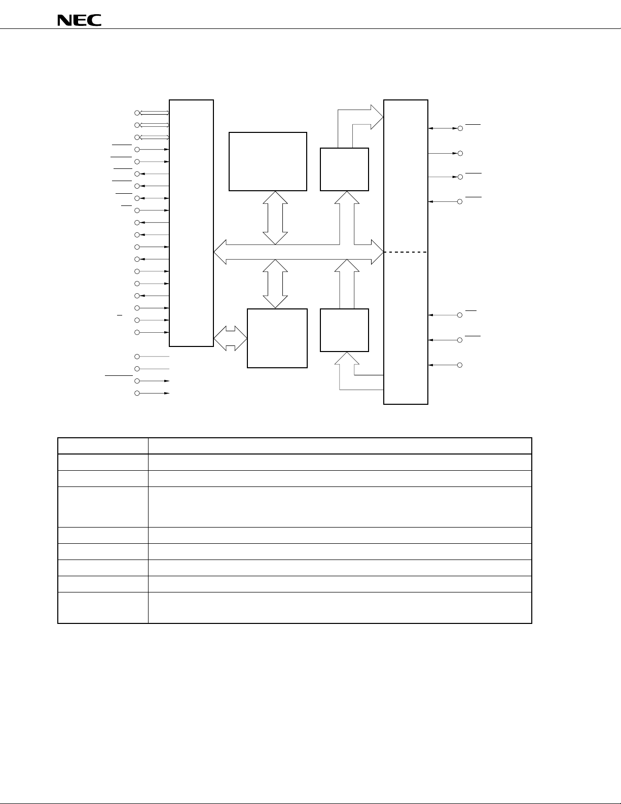
BLOCK DIAGRAM
D0-D7
A16D8
-A23D15
A0-A15
IORD
IOWR
MRD
MWR
UBE
CS
ASTB
AEN
READY
HLDRQ
HLDAK
CRQ
INT
CLRINT
B/W
PU
VCC
GND
RESET
CLK
Bus
interface
Internal controller
Internal bus
DMAC
TxFIFO
RxFIFO
Transmitter
Receiver
µ
TxC
TxD
RTS
CTS
CD
RxC
RxD
PD72107
Name Function
Bus interface An interface between the µPD72107 and external memory or external host processor
Internal controller Manages LAP-B protocol including control of the DMAC block, transmitter block, and receiver block
DMAC Controls the transfer of data on the external memory to the internal controller or transmitter block,
(Direct Memory and controls the writing of data in the internal controller or receiver block to the external memory
Access Controller)
TxFIFO A 16-byte buffer for when transmit data is sent from the DMAC to the transmitter block
RxFIFO A 32-byte buffer for when receive data is sent from the receiver block to the DMAC
Transmitter Converts the contents of TxFIFO into an HDLC frame and transmits it as serial data
Receiver Receives HDLC frame and writes internal data to RxFIFO
Internal bus An 8-bit address bus and 8-bit data bus that connect the internal controller, DMAC, FIFO, serial block,
and bus interface block
2
Page 3
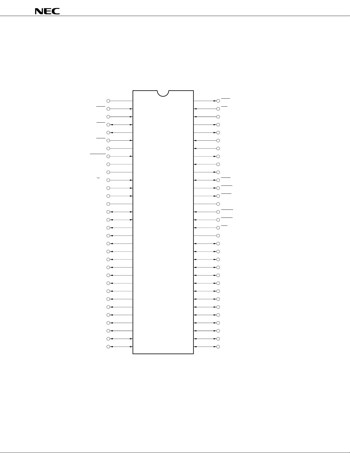
PIN CONFIGURATION (Top View)
64-pin plastic shrink DIP (750 mils)
µ
PD72107CW
µ
PD72107
RxC
RxD
TxC
TxD
CTS
RESET
NC
B/W
PU
CLK
GND
A0
A1
A2
A3
A4
A5
A6
A7
A8
A9
A10
A11
A12
A13
A14
A15
A16D8
A17D9
IC
IC
IC
1
2
3
4
5
6
7
8
9
10
11
12
13
14
15
16
17
18
19
20
21
22
23
24
25
26
27
28
29
30
31
32
64
63
62
61
60
59
58
57
56
55
54
53
52
51
50
49
48
47
46
45
44
43
42
41
40
39
38
37
36
35
34
33
RTS
CD
CRQ
AEN
ASTB
READY
HLDAK
HLDRQ
CLRINT
INT
UBE
MWR
MRD
GND
IOWR
IORD
CS
CC
V
D7
D6
D5
D4
D3
D2
D1
D0
A23D15
A22D14
A21D13
A20D12
A19D11
A18D10
3
Page 4
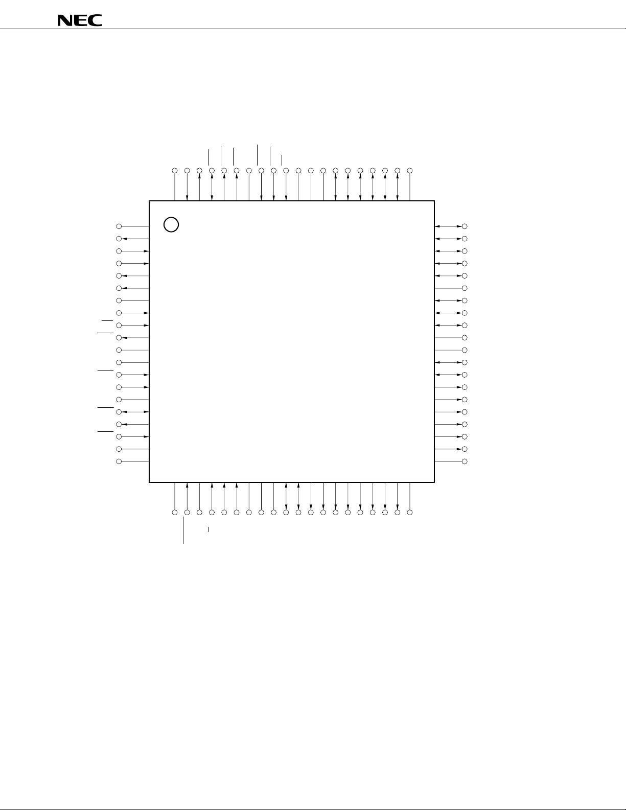
80-pin plastic QFP (14 × 14 mm)
µ
PD72107GC-3B9
NC
CLRINT
INT
80 79 78 77 76 75 74 73 72 71 70 69 68 67 66 65 64 63 62 61
UBE
MWR
MRD
GND
IOWR
IORDCSVCCNCVCCD7D6D5D4D3D2
NC
µ
PD72107
NC
HLDRQ
HLDAK
READY
ASTB
AEN
NC
CRQ
CD
RTS
NC
IC
RxC
RxD
NC
TxC
TxD
CTS
IC
NC
1
2
3
4
5
6
7
8
9
10
11
12
13
14
15
16
17
18
19
20
21 22 23 24 25 26 27 28 29 30 31 32 33 34 35 36 37 38 39 40
NC
IC
RESET
B/W
PU
CLK
GND
A0A1A2A3A4A5A6A7A8
NC
GND
A9
NC
60
59
58
57
56
55
54
53
52
51
50
49
48
47
46
45
44
43
42
41
D1
D0
A23D15
A22D14
A21D13
NC
A20D12
A19D11
A18D10
NC
NC
A17D9
A16D8
A15
A14
A13
A12
A11
A10
NC
4
Page 5
68-pin plastic QFJ (950 × 950 mils)
Q
µ
PD72107L
IC
CTS
TxD
9876543216867666564636261
RESET
IC
B/W
PU
CLK
GND
GND
A0
A1
A2
A3
A4
A5
A6
A7
A8
A9
10
11
12
13
14
15
16
17
18
19
20
21
22
23
24
25
26
27 28 29 30 31 32 33 34 35 36 37 38 39 40 41 42 43
TxCNCRxD
RxCICNC
RTSCDCRQ
AEN
ASTB
READY
HLDAK
HLDR
60
59
58
57
56
55
54
53
52
51
50
49
48
47
46
45
44
µ
PD72107
CLRINT
INT
UBE
MWR
MRD
GND
IOWR
IORD
CS
V
CC
VCC
D7
D6
D5
D4
D3
D2
A10
A11
A12
A13
A14
A15
A16D8
A17D9
NC
A18D10
A19D11
A20D12
A21D13
A22D14
A23D15
D0
D1
5
Page 6
1. PINS
1.1 Pin Functions
µ
PD72107
SDIP QFP QFJ Active
Pin No. Pin No. Pin No. Level
V
CC 47 68 50 – – +5 V power supply
70 51
GND 14 27 15 – – Ground (0 V)
51 28 16 Note that there is more than one ground pin.
74 55
CLK 13 26 14 I – System clock input
(Clock) Input clock of 1 MHz to 8.2 MHz.
RESET 8 22 10 I L Initializes the internal
(Reset) more than 7 CLK clock cycles is required (clock
PU 12 25 13 I – Pull up to high level when using in normal operation.
(Pull Up)
CS 48 71 52 I L When bus master
(Chip Select) Set to disable.
MRD 52 75 56 O L When bus master
(Memory Read) 3-state Reads the data of the external memory at low level.
MWR 53 76 57 O L When bus master
(Memory Write) 3-state Writes the data to the external memory at low level.
IORD 49 72 53 I L This pin is used when the external host processor
(I/O Read) reads the contents of the internal registers of the
IOWR 50 73 54 I L This pin is used when the external host processor
(I/O Write) writes the data to the internal registers of the
ASTB 60 5 64 O H This pin is used to latch the address output from
(Address Strobe) the
I/OPin Name Function
µ
PD72107. Active width of
input is required).
After reset, this pin becomes a bus slave.
When bus slave
Read/write operation from the host processor at low
level is enabled.
When bus slave
High impedance
When bus slave
High impedance
µ
PD72107.
µ
PD72107.
µ
PD72107 externally.
6
Page 7
µ
PD72107
SDIP QFP QFJ Active
Pin No. Pin No. Pin No. Level
NC 9 1, 7, 1 – – Use this pin open.
(No Connection) 11, 15, 5
20, 21, 35
29, 40,
41, 50,
51, 55,
61, 69,
80
IC 1 12 2 – – Do not connect anything to this pin.
(Internally 7 19 9
Connected) 10 23 11
UBE 54 77 58 I/O L/H When bus master (output)
(Upper Byte 3-state The signal output from this pin changes according
Enable) to the input value of the B/W pin.
I/OPin Name Function
• Byte transfer mode (B/W = 0)
UBE is always high impedance.
• Word transfer mode (B/W = 1)
Indicates that valid data is either in pins D0 to D7
or pins A16D8 to A23D15 (or both).
UBE A0 D0 to D7 A16D8 to A23D15
00
01 ×
10 ×
11 ××
When bus slave (input)
UBE pin becomes input, and indicates that valid
data is either in pins D0 to D7 or pins A16D8 to
A23D15.
UBE A0 D0 to D7 A16D8 to A23D15
00 ×
01 ×
10 ×
11 ×
7
Page 8
µ
PD72107
SDIP QFP QFJ Active
Pin No. Pin No. Pin No. Level
B/W 11 24 12 I L/H Specifies the data bus that accesses the external
(Byte/Word) memory when bus master.
READY 59 4 63 I H An input signal that is used to extend the MRD and
(Ready) MWR signal widths output by the µPD72107 to
HLDRQ 57 2 61 O H A hold request signal to the external host processor.
(Hold Request) When a DMA operation is performed in the µPD72107,
HLDAK 58 3 62 I H A hold acknowledge signal from the external host
(Hold Acknowledge)
AEN 61 6 65 O H When bus master, this signal enables the latched
(Address Enable) higher addresses and outputs them to system ad-
A0, A1 15, 16 30, 31 17, 18 I/O – Bidirectional 3-state address lines.
A2 to A15 17 to 30 32 to 47 19 to 32 O – When bus master
(except 3-state Output bit 2 to bit 15 of memory access addresses.
40, 41) When bus slave
I/OPin Name Function
B/W = 0 Byte units (8 bits)
B/W = 1 Word units (16 bits)
After power-on, fix the status of the B/W pin.
In the case of word access, the lower data bus is the
contents data of even addresses.
adapt to low-speed memory. When the READY
signal is low level, the MRD and MWR signals
maintain active low. Do not change the READY
signal at any time other than the specified setup/
hold time.
this signal is activated to switch from bus slave to
bus master.
processor. When the µPD72107 detects that this
signal is active, the bus slave switches to bus
master, and a DMA operation is started.
dress bus. This signal is also used for disabling
other system bus drivers.
3-state When bus master (output)
Indicate the lower 2-bit addresses of memory access.
When bus slave (input)
Input addresses when the external host processor
I/O accesses the µPD72107.
Become high impedance.
8
Page 9
µ
PD72107
SDIP QFP QFJ Active
Pin No. Pin No. Pin No. Level
A16D8 to A23D15 31 to 38 48 to 58 33 to 41 I/O – Bidirectional 3-state address/data buses. Multiplex
(except 50, (except 35)
51, 55) and the higher 8 bits to 15 bits of data.
D0 to D7 39 to 46 59 to 67 42 to 49 I/O – Bidirectional 3-state data buses.
(except 61)
CRQ 62 8 66 I H A signal requesting command execution to the
(Command
Request)
INT 55 78 59 O H An interrupt signal from the µPD72107 to the
(Interrupt) external host processor.
CLRINT 56 79 60 I H A signal inactivating the INT signal being output by
(Clear Interrupt) the µPD72107. The µPD72107 generates the CLRINT
CTS 6 18 8 I – A general-purpose input pin.
(Clear To Send) The µPD72107 reports the “CTS pin change detection
I/OPin Name Function
3-state pins of the higher 16 bits to 23 bits of addresses
3-state When bus master
When writing to external memory, these pins become
input if reading at output.
When bus slave
Usually, these pins become high impedance. When
the external host processor reads I/O of the µPD72107,
the internal register data is output.
µ
PD72107 by the external host processor. The
µ
PD72107 starts fetching commands from on the
external memory at the rising edge of this signal.
signal in the LSI internal circuit at the rising edge of
this signal, and forcibly makes the INT output signal
low.
status” to the external host processor when the
input level of this pin is changed in the generalpurpose input/output pin support (setting RSSL to
1 by the “system initialization command”). The
change of input level is recognized only when the
same level is sampled twice in succession after
sampling in 8-ms cycles and detecting the change.
Moreover, when the external host processor issues
a “general-purpose input/output pin read command”
to the µPD72107, the µPD72107 reports the pin
information of this pin to the external host processor
by a “general-purpose input/output pin read response
status”.
The change can be detected even in the clock input
stop status of TxC and RxC.
9
Page 10
µ
PD72107
SDIP QFP QFJ Active
Pin No. Pin No. Pin No. Level
RTS 64 10 68 O – A general-purpose output pin.
(Request To Send)
CD 63 9 67 I – A general-purpose input pin.
(Carrier Detect) The µPD72107 reports the “CD pin change detection
TxD 5 17 7 O – A serial transmit data output pin.
(Transmit Data)
TxC 4 16 6 I/O – When CLK is set to 01 or 10 by “operation mode
(Transmit Clock) 3-state setting LCW” (output)
I/OPin Name Function
The output value of this pin can be changed by
issuing an “RTS pin write command” from the external
host processor to the µPD72107. Moreover, when
the external host processor issues a “general-purpose
input/output pin read command” to the µPD72107,
the µPD72107 reports the pin information of this pin
to the external host processor by a “general-purpose
input/output pin read response status”.
status” to the external host processor when the
input level of this pin is changed in the generalpurpose input/output pin support (setting RSSL to
1 by the “system initialization command”). The
change of input level is recognized only when the
same level is sampled twice in succession after
sampling in 8-ms cycles and detecting the change.
Moreover, when the external host processor issues
a “general-purpose input/output pin read command”
to the µPD72107, the µPD72107 reports the pin
information of this pin to the external host processor
by a “general-purpose input/output pin read response
status”.
The change can be detected even in the clock input
stop status of TxC and RxC.
Outputs a clock that divides by 16 the input signal
of the RxC pin or CLK pin made by the µPD72107.
Caution TxC becomes input because CLK = 00
is the default after reset. It becomes
output after setting CLK to 01 or 10 by
“operation mode setting LCW”.
When CLK is set to 00 by “operation mode setting
LCW” (input)
Inputs transmit clock externally.
Remark LCW: abbreviation for Link Command Word
10
Page 11

µ
PD72107
SDIP QFP QFJ Active
Pin No. Pin No. Pin No. Level
RxD 3 14 4 I – A serial receive data input pin.
(Receive Data)
RxC 2 13 3 I – When CLK is set to 01 or 10 by “operation mode
(Receive Clock) setting LCW”
I/OPin Name Function
Sixteen times the clock input of the transmit/receive
clock for the on-chip DPLL of the
When CLK is set to 00 by “operation mode setting
LCW”
One time the clock input of the receive clock
µ
PD72107
Remark LCW: abbreviation for Link Command Word
1.2 Pin Status after Reset of µPD72107
The status of the output pins and input/output pins after reset in the µPD72107 is as shown in Table 1-1.
Table 1-1. Pin Status after Reset
Pin Number
64-pin SDIP 80-pin QFP 68-pin QFJ
4 16 6 TxC I/O
5 17 7 TxD O H
15, 16 30, 31 17, 18 A0, A1 I/O
17 to 30 32 to 47 19 to 32 A2 to A15 O
(except 40, 41)
31 to 38 48 to 58 33 to 41 A16D8 to A23D15 I/O
(except 50, 51, 55) (except 35)
39 to 46 59 to 67 42 to 49 D0 to D7 I/O
(except 61)
52 75 56 MRD O
53 76 57 MWR O
54 77 58 UBE I/O
55 78 59 INT O L
57 2 61 HLDRQ O L
60 5 64 ASTB O L
61 6 65 AEN O L
64 10 68 RTS O H
Pin Name
I/O
Note
Note
Note
Note
Note
Note
Note
Note
During Reset
High impedance
High impedance
High impedance
High impedance
High impedance
High impedance
High impedance
High impedance
Note 3-state
Remarks 1. The status after reset is released is the same as the status during reset.
2. Input low level to the RESET pin for more than 7 clocks of the system clock.
11
Page 12

µ
PD72107
2. ELECTRICAL SPECIFICATIONS
Absolute Maximum Ratings (TA = +25°C)
Parameter Symbol Conditions Ratings Unit
Power supply voltage VDD –0.5 to +7.0 V
Input voltage VI –0.5 to VDD + 0.3 V
Output voltage VO –0.5 to VDD + 0.3 V
Operating ambient temperature TA –40 to +85 °C
Storage temperature Tstg –40 to +125 °C
Caution Product quality may suffer if the absolute maximum rating is exceeded even momentarily for
any parameter. That is, the absolute maximum ratings are rated values at which the product
is on the verge of suffering physical damage, and therefore the product must be used under
conditions that ensure that the absolute maximum ratings are not exceeded.
DC Characteristics (T
Parameter Symbol Conditions MIN. TYP. MAX. Unit
Input voltage, low VILC CLK pin –0.5 +0.8 V
Input voltage, high VIHC CLK and PU pins +3.3 VDD + 0.3 V
Output voltage, low VOL IOL = 2.5 mA 0.4 V
Output voltage, high VOH IOH = –400 µA 0.7 × VDD V
Power supply current IDD At operation 20 50 mA
Input leakage current ILI 0 V ≤ VIN ≤ VDD ±10
Output leakage current ILO 0 V ≤ VOUT ≤ VDD ±10
A = –40 to +85°C, VDD = 5 V ±10%)
VIL Other pins –0.5 +0.8 V
VIH Other pins +2.2 VDD + 0.3 V
µ
A
µ
A
Capacitance (TA = +25°C, VDD = 0 V)
Parameter Symbol Conditions MIN. TYP. MAX. Unit
Input capacitance CI fC = 1 MHz – 8 15 pF
Output capacitance CO Unmeasured pins returned to 0 V – 8 15 pF
I/O capacitance CIO –820pF
12
Page 13

µ
PD72107
AC Characteristics (TA = –40 to +85°C, VDD = 5 V ±10%)
When bus master (1)
Parameter Symbol Conditions MIN. MAX. Unit
CLK cycle time tCYK 121 1000 ns
CLK low-level time tKKL 50 ns
CLK high-level time tKKH 50 ns
CLK rise time tKR 1.5 – 3.0 V 10 ns
CLK fall time tKF 3.0 – 1.5 V 10 ns
Load condition
DUT
C
L = 50 pF
CL includes jig capacitance.
Caution If the load capacitance exceeds 50 pF due to the configuration of the circuit, keep the load
capacitance of this device to within 50 pF by inserting a buffer or by some other means.
Remark DUT: device under test
AC test input/output waveform (except clock)
2.4 V
2.2 V
Test points
0.8 V
0.4 V
2.2 V
0.8 V
System clock
CLK
tKF tKR
tKKL
1.5 V
tCYK
3.0 V
tKKH
13
Page 14

µ
PD72107
When bus master (2)
Parameter Symbol Conditions MIN. MAX. Unit
HLDRQ ↑ delay time (vs. CLK ↓)tDHQH 100 ns
HLDRQ ↓ delay time (vs. CLK ↑)tDHQL 100 ns
HLDAK setup time (vs. CLK ↑)tSHA 35 ns
HLDAK hold time (vs. CLK ↑)tHHA 20 ns
AEN ↑ delay time (vs. CLK ↓)tDAEH 100 ns
AEN ↓ delay time (vs. CLK ↑)tDAEL 100 ns
ASTB ↑ delay time (vs. CLK ↑)tDSTH 70 ns
ASTB high-level width tSTSTH tKKH–15 ns
ASTB ↓ delay time (vs. CLK ↓)tDSTL 100 ns
ADR/UBE/MRD/MWR delay time tDA 100 ns
(vs. CLK ↑)
ADR/UBE/MRD/MWR float time tFA 70 ns
(vs. CLK ↑)
ADR setup time (vs. ASTB ↓)tSAST tKKH–35 ns
ADR hold time (vs. ASTB ↓)tHSTA tKKL–20 ns
MRD ↓ delay time (vs. ADR float) tDAR 0ns
MRD ↓ delay time (vs. CLK ↑)tDRL 70 ns
MRD low-level width tRRL2 2t CYK–50 ns
MRD ↑ delay time (vs. CLK ↑)tDRH 70 ns
Data setup time (vs. MRD ↑)tSDR 100 ns
Data hold time (vs. MRD ↑)tHRD 0ns
MWR ↓ delay time (vs. CLK ↑)tDWL 70 ns
MWR low-level width tWWL2 2tCYK–50 ns
MWR ↑ delay time (vs. CLK ↑)tDWH 70 ns
READY setup time (vs. CLK ↑)tSRY 35 ns
READY hold time (vs. CLK ↑)tHRY 20 ns
14
Page 15

tDHQH
tSHA
tHHA
tDAEH
tDSTH
tDSTL
tDA
tSTSTH
tSAST tHSTA
tDWL
tFA
tSRY tSRY
tDA
tDAR
tDRL
tRRL2
tDRH
tSDR
tHRD
tFA
tHRY tDWHtHRY
tWWL2
tDAEL
tDHQL
Hi-Z
Hi-Z
Hi-Z
Hi-Z
Hi-ZHi-Z
Hi-Z
Hi-Z
Hi-Z
Hi-Z
Address
Input data
Output data
Address
CLK
HLDRQ
HLDAK
AEN
ASTB
A16D8-A23D15
A0, A1/A2-A15
UBE
MWR
READY
A16D8-A23D15
MRD
Address
tHHA
When bus master
15
µ
PD72107
Page 16

µ
PD72107
When bus slave (1)
Parameter Symbol Conditions MIN. MAX. Unit
IOWR low-level width tWWL 100 ns
CS low-level hold time tHWCS 0ns
(vs. IOWR ↑)
ADR/UBE/CS low-level setup time tSAW 0ns
(vs. IOWR ↓)
ADR/UBE hold time (vs. IOWR ↑)tHWA 0ns
Data setup time (vs. IOWR ↑)tSDW 100 ns
Data hold time (vs. IOWR ↑)tHWD 0ns
IORD low-level width tRRL 150 ns
ADR/CS low-level setup time tSAR 35 ns
(vs. IORD ↓)
ADR/CS low-level hold time tHRA 0ns
(vs. IORD ↑)
Data delay time (vs. IORD ↓)tDRD 120 ns
Data float time (vs. IORD ↑)tFRD 10 100 ns
RESET low-level width tRSTL 7tCYK ns
VDD setup time (vs. RESET ↑)tSVDD 1000 ns
RESET ↑ –1st • IOWR/IORD tSYWR 2tCYK ns
IOWR/IORD recovery time tRVWR 200 ns
16
Page 17

When bus slave
A0-A23
CS
IOWR
t
SAW
t
WWL
t
HWA
t
HWCS
µ
PD72107
UBE
D0-D15
CS
A0-A23
IORD
D0-D15
t
t
SDW
t
SAR
t
DRD
t
RRL
HWD
t
HRA
t
FRD
Hi-Z Hi-Z
V
RESET
IORD/IOWR
IORD
IOWR
DD
t
RVWR
t
RVWR
t
SVDD
t
RSTL
t
RVWR
t
SYWR
t
RVWR
17
Page 18

µ
PD72107
When bus slave (2)
Parameter Symbol Conditions MIN. MAX. Unit
IOWR/IORD high-level setup time tSWR –20 ns
(vs. HLDAK ↑)
IOWR/IORD high-level hold time t HWR 100 ns
(vs. AEN ↓)
HLDAK
tSWR
IOWR/IORD
AEN
tHWR
IOWR/IORD
When bus slave (3)
Parameter Symbol Conditions MIN. MAX. Unit
CLRINT high-level width tCLCLH 100 ns
INT ↑ delay time (vs. CLK ↑)tDIH 100 ns
INT ↓ delay time (vs. CLRINT ↑)tDIL 100 ns
CRQ high-level width tCRCRH 100 ns
CLK
CLRINT
tCLCLH
18
INT
CRQ
tDIH
tDIL
tCRCRH
Page 19

µ
PD72107
Serial block (1)
Parameter Symbol Conditions MIN. MAX. Unit
TxC/RxC cycle time tCYS When on-chip DPLL is not used 250 DC ns
TxC/RxC low-level time tSSL 110 ns
TxC/RxC high-level time tSSH 110 ns
TxC/RxC rise time tSR 20 ns
TxC/RxC fall time tSF 12 ns
TxD delay time (vs. TxC ↓)tDTXD 100 ns
RxD setup time (vs. RxC ↑)tSRXD 50 ns
RxD hold time (vs. RxC ↑)tHRXD 70 ns
Serial clock (when on-chip DPLL is not used)
TxC/RxC
TxC (input)
TxD
RxC
RxD
tSF tSR
0.8 V
tSRXD tHRXD
tSSL
tCYS
tDTXD tDTXD
t
2.2 V
SSH
19
Page 20

µ
PD72107
Serial block (2)
Parameter Symbol Conditions MIN. MAX. Unit
RxC cycle time tCYR When on-chip DPLL is used (source clock = RxC) 30.3 ns
When on-chip DPLL is used (source clock = CLK) 125 1000
RxC low-level time tSSRL When on-chip DPLL is used (source clock = RxC) 10 ns
When on-chip DPLL is used (source clock = CLK) 50
RxC high-level time tSSRH When on-chip DPLL is used (source clock = RxC) 10 ns
When on-chip DPLL is used (source clock = CLK) 50
RxC rise time tSRR When on-chip DPLL is used (source clock = RxC) 5 ns
When on-chip DPLL is used (source clock = CLK) 10
RxC fall time tSRF When on-chip DPLL is used (source clock = RxC) 5 ns
When on-chip DPLL is used (source clock = CLK) 10
Transmit/receive data cycle tCYD When on-chip DPLL is used (source clock = RxC) 500 ns
When on-chip DPLL is used (source clock = CLK) 2000 16000
TxC low-level time tTCTCL When on-chip DPLL is used
TxC high-level time tTCTCH
TxD delay time (vs. TxC ↓)tDTCTD 50 ns
TxD hold time (vs. TxC ↑)tHTCTD
0.5tCYD–25
0.5tCYD–25
0.5tCYD–25
ns
ns
ns
Serial clock (when on-chip DPLL is used)
tCYR
tSSRL
tSRF
RxC
TxC
tTCTCL
tDTCTD
TxD
tSSRH
tSRR
tTCTCH
tHTCTD
tCYD
20
Page 21

µ
PD72107
Serial block (3)
Parameter Symbol Conditions MIN. MAX. Unit
RTS ↑ delay time (vs. CLK ↑)tDRTH 100 ns
RTS ↓ delay time (vs. CLK ↑)tDRTL 100 ns
CD setup time (vs. CLK ↑)tSCD 35 ns
CD hold time (vs. CLK ↑)tHCD 20 ns
CTS setup time (vs. CLK ↑)tSCT 35 ns
CTS hold time (vs. CLK ↑)tHCT 20 ns
CLK
RTS
tDRTL
tHCD
tDRTH
CD
CTS
tSCD
tHCT
tSCT
21
Page 22

3. APPLICATION CIRCUIT EXAMPLE
(1) Connection with SIFC (µPD98201)
µµ
PD72107 PD98201
TxD BINA
µ
PD72107
RxD
TxC
RxC
BOUT1
SIFCLAP-B
BCLK
22
Page 23

µ
PD72107 System Configuration Example (Local Memory Type)
Local memory 64 Kbytes
Host processor PD72107
RD WR CS UBE A0-A15 D0-D15
µ
4. SYSTEM CONFIGURATION EXAMPLES
MEMR
MEMW
IOR
IOW
AB0-AB7
AB8-AB15
AB16-AB19
BHE
DB0-DB15
INT
Local
bus request
WAIT
A B
µ
PD71086
OE
A B
µ
PD71086
OE
A B
µ
PD71086
OE
A B
µ
PD71086
OE
Access
contention
resolution
circuit
Decoder
A0-A15
D0-D15
MRD
MWR
IORD
IOWR
CS
A0-A15
D0-D7
A16D8-A23D15
UBE
AEN
INT
HLDRQ
HLDAK
µ
PD72107
23
Page 24

24
µ
PD72107 System Configuration Example (Main Memory Sharing Type)
Host processor PD72107
INTP
µ
PD70116
AD8-AD15
INT
INTAK
RD
WR
HLDRQ
HLDAK
ASTB
A16-A19
AD0-AD7
UBE
BUF R/W
BUFEN
INT
INTAK
PD71059
µ
RD WR D0-D7
STB OE
µ
PD71082×3
CS
A0
A16-A19
Decoder
A0-A15
D8-D15
OE STB
µ
PD71082
µ
INT
IORD
IOWR
CS
MRD
MWR
HLDRQ
HLDAK
AEN
ASTB
D0-D7
A16D8-A23D15
A0-A15
UBE
µ
PD71086×2
TOE
D0-D7
RD WR CS UBE
Memory
D0-D7 D8-D15
µ
PD72107
Page 25

I
J
G
H
F
D
N
M
CB
M
R
64 33
321
K
L
NOTES
1. Controlling dimension millimeter.
P64C-70-750A,C-3
ITEM MILLIMETERS INCHES
B
C
D
F
G
H
J
K
1.778 (T.P.)
3.2±0.3
0.51 MIN.
1.78 MAX.
L
M
0.17
0.25
19.05 (T.P.)
5.08 MAX.
17.0±0.2
N
0 to 15°
0.50±0.10
0.9 MIN.
R
0.070 MAX.
0.020
0.035 MIN.
0.126±0.012
0.020 MIN.
0.200 MAX.
0.750 (T.P.)
0.669
0.010
0.007
0 to 15°
+0.004
–0.003
0.070 (T.P.)
+0.10
–0.05
+0.004
–0.005
64 PIN PLASTIC SHRINK DIP (750 mil)
2. Each lead centerline is located within 0.17 mm (0.007 inch) of
its true position (T.P.) at maximum material condition.
3. Item "K" to center of leads when formed parallel.
A 58.0 2.283
+0.028
–0.008
+0.68
–0.20
I 4.05 0.159
+0.011
–0.008
+0.26
–0.20
A
+0.009
–0.008
5. PACKAGE DRAWINGS
µ
PD72107
25
Page 26

80 PIN PLASTIC QFP (14x14)
µ
PD72107
A
B
61
60
41
40
CD
80
1
20
21
F
G
M
H
I
P
J
K
N
L
NOTE
Each lead centerline is located within 0.13 mm (0.005 inch) of
its true position (T.P.) at maximum material condition.
detail of lead end
S
Q
R
M
ITEM MILLIMETERS INCHES
A 17.2±0.4 0.677±0.016
B 14.0±0.2 0.551
C 14.0±0.2 0.551
D 17.2±0.4 0.677±0.016
F 0.825 0.032
G 0.825 0.032
H 0.30±0.10 0.012
I 0.13 0.005
J 0.65 (T.P.) 0.026 (T.P.)
K 1.6±0.2 0.063±0.008
L 0.8±0.2 0.031
M 0.15 0.006
N 0.10 0.004
P
Q 0.1±0.1 0.004±0.004
R5°±5° 5°±5°
S 3.0 MAX. 0.119 MAX.
+0.10
–0.05
2.7±0.1 0.106
+0.009
–0.008
+0.009
–0.008
+0.004
–0.005
+0.009
–0.008
+0.004
–0.003
+0.005
–0.004
S80GC-65-3B9-5
26
Page 27

68 PIN PLASTIC QFJ (950 x 950 mil)
A
B
68
1
CD
µ
PD72107
G
H
J
F
S
K
M
M
N
P
I
NOTES
1. Controlling dimension millimeter.
2. Each lead centerline is located within 0.12 mm of
its true position (T.P.) at maximum material condition.
E
Q
U
T
S
ITEM MILLIMETERS INCHES
A 25.2±0.2 0.992±0.008
B 24.20±0.1 0.953
C 24.20±0.1 0.953
D 25.2±0.2 0.992±0.008
E 1.94±0.15 0.076
F 0.6 0.024
G 4.4±0.2 0.173
H 2.8±0.2 0.110
I 0.9 MIN. 0.035 MIN.
J 3.4±0.1 0.134
K 1.27 (T.P.) 0.050 (T.P.)
M 0.42±0.08 0.017
N 0.12 0.005
P 23.12±0.2 0.910
Q 0.15 0.006
T R 0.8 R 0.031
U 0.22 0.009
+0.08
−0.07
+0.004
−0.005
+0.004
−0.005
+0.007
−0.006
+0.009
−0.008
+0.009
−0.008
+0.004
−0.005
+0.003
−0.004
+0.009
−0.008
+0.003
−0.004
P68L-50A1-3
27
Page 28

µ
PD72107
6. RECOMMENDED SOLDERING CONDITIONS
The µPD72107 should be soldered and mounted under the following recommended conditions.
For the details of the recommended soldering conditions, refer to the document Semiconductor Device
Mounting Technology Manual (C10535E).
For soldering methods and conditions other than those recommended below, contact your NEC sales representative.
Surface mounting type
µ
PD72107GC-3B9: 80-pin plastic QFP (14 × 14 mm)
•
Soldering Method Soldering Conditions Recommended Condition Symbol
Infrared reflow Package peak temperature: 235°C, Time: 30 sec. Max. IR35-00-3
(at 210°C or higher), Count: three times or less
VPS Package peak temperature: 215 °C, Time: 40 sec. Max. VP15-00-3
(at 200°C or higher), Count: three times or less
Wave soldering Solder bath temperature: 260°C, Time: 10 sec. Max., WS60-00-1
Count: one time, Preheating temperature: 120°C Max.
(package surface temperature)
Partial heating Pin temperature: 300°C Max., Duration: 3 sec. Max. (per pin row) –
Caution Do not use different soldering methods together (except for partial heating).
•
µ
PD72107L: 68-pin plastic QFJ (950 × 950 mils)
Soldering Method Soldering Conditions Recommended Condition Symbol
VPS Package peak temperature: 215 °C, Time: 40 sec. Max. VP15-00-1
(at 200°C or higher), Count: one time
Partial heating Pin temperature: 300°C Max., Duration: 3 sec. Max. (per pin row) –
Insertion type
•
µ
PD72107CW: 64-pin plastic shrink DIP (750 mils)
Soldering Method Soldering Conditions
Wave soldering (pin only) Solder bath temperature: 260°C Max., Time: 10 sec. Max.
Partial heating Pin temperature: 300°C Max., Duration: 3 sec. Max. (per a pin)
Caution Wave soldering must be applied only to pins. Be sure to avoid jet soldering the package body.
28
Page 29

[MEMO]
µ
PD72107
29
Page 30

[MEMO]
µ
PD72107
30
Page 31

µ
NOTES FOR CMOS DEVICES
1 PRECAUTION AGAINST ESD FOR SEMICONDUCTORS
Note: Strong electric field, when exposed to a MOS device, can cause destruction
of the gate oxide and ultimately degrade the device operation. Steps must
be taken to stop generation of static electricity as much as possible, and
quickly dissipate it once, when it has occurred. Environmental control must
be adequate. When it is dry, humidifier should be used. It is recommended
to avoid using insulators that easily build static electricity. Semiconductor
devices must be stored and transported in an anti-static container, static
shielding bag or conductive material. All test and measurement tools
including work bench and floor should be grounded. The operator should
be grounded using wrist strap. Semiconductor devices must not be touched
with bare hands. Similar precautions need to be taken for PW boards with
semiconductor devices on it.
PD72107
2 HANDLING OF UNUSED INPUT PINS FOR CMOS
Note: No connection for CMOS device inputs can be cause of malfunction. If no
connection is provided to the input pins, it is possible that an internal input
level may be generated due to noise, etc., hence causing malfunction. CMOS
device behave differently than Bipolar or NMOS devices. Input levels of
CMOS devices must be fixed high or low by using a pull-up or pull-down
circuitry. Each unused pin should be connected to VDD or GND with a
resistor, if it is considered to have a possibility of being an output pin. All
handling related to the unused pins must be judged device by device and
related specifications governing the devices.
3 STATUS BEFORE INITIALIZATION OF MOS DEVICES
Note: Power-on does not necessarily define initial status of MOS device. Produc-
tion process of MOS does not define the initial operation status of the device.
Immediately after the power source is turned ON, the devices with reset
function have not yet been initialized. Hence, power-on does not guarantee
out-pin levels, I/O settings or contents of registers. Device is not initialized
until the reset signal is received. Reset operation must be executed immediately after power-on for devices having reset function.
31
Page 32

µ
PD72107
The export of this product from Japan is prohibited without governmental license. To export or re-export this product from
a country other than Japan may also be prohibited without a license from that country. Please call an NEC sales
representative.
No part of this document may be copied or reproduced in any form or by any means without the prior written
consent of NEC Corporation. NEC Corporation assumes no responsibility for any errors which may appear in
this document.
NEC Corporation does not assume any liability for infringement of patents, copyrights or other intellectual property
rights of third parties by or arising from use of a device described herein or any other liability arising from use
of such device. No license, either express, implied or otherwise, is granted under any patents, copyrights or other
intellectual property rights of NEC Corporation or others.
While NEC Corporation has been making continuous effort to enhance the reliability of its semiconductor devices,
the possibility of defects cannot be eliminated entirely. To minimize risks of damage or injury to persons or
property arising from a defect in an NEC semiconductor device, customers must incorporate sufficient safety
measures in its design, such as redundancy, fire-containment, and anti-failure features.
NEC devices are classified into the following three quality grades:
"Standard", "Special", and "Specific". The Specific quality grade applies only to devices developed based on a
customer designated "quality assurance program" for a specific application. The recommended applications of
a device depend on its quality grade, as indicated below. Customers must check the quality grade of each device
before using it in a particular application.
Standard: Computers, office equipment, communications equipment, test and measurement equipment,
audio and visual equipment, home electronic appliances, machine tools, personal electronic
equipment and industrial robots
Special: Transportation equipment (automobiles, trains, ships, etc.), traffic control systems, anti-disaster
systems, anti-crime systems, safety equipment and medical equipment (not specifically designed
for life support)
Specific: Aircrafts, aerospace equipment, submersible repeaters, nuclear reactor control systems, life
support systems or medical equipment for life support, etc.
The quality grade of NEC devices is "Standard" unless otherwise specified in NEC's Data Sheets or Data Books.
If customers intend to use NEC devices for applications other than those specified for Standard quality grade,
they should contact an NEC sales representative in advance.
Anti-radioactive design is not implemented in this product.
M4 96.5
2
 Loading...