

Page 1
DATA SHEET
MOS INTEGRATED CIRCUIT
µ
PD6379, 6379A, 6379L, 6379AL
2-CHANNEL 16-BIT D/A CONVERTER FOR AUDIO APPLICATION
The µPD6379 and 6379A are 2-channel 16-bit D/A converters for digital audio signal demodulation. These D/A
µ
converters employ the resistor string conversion method which has been tested by existing model
are more compact and require fewer external components than the µPD6376. In addition, low-voltage models, the
µ
PD6379L and 6379AL (minimum operating supply voltage = +3.0 V) are also available for applications in portable
systems.
FEATURES
• Resistor string conversion method
• 0-point digital shift circuit
• × 4 oversampling
Sampling frequency: 200 kHz MAX.
• Signal processing format for 2’s complement, MSB first, and backward justification data accommodated
• Left and right in-phase output
• High performance (at V
S/N ratio: 100 dB TYP.
Dynamic range: 96 dB TYP.
• Low-voltage models available
• Bipolar LR clock (LRCK)
• Low power dissipation:10 mW TYP.
µ
PD6379L, 6379AL at VDD = +3.3 V)
(with
DD = +5.0 V)
PD6376 but they
Supply voltage when L-ch data is input when L-ch data is input
+3.3 V (VDD = +3.0 to 5.5 V)
+5.0 V (VDD = +4.5 to 5.5 V)
• Few external components
Internal output operational amplifier
Only one electrolytic capacitor required for smoothing reference voltage, instead of two capacitors required by
existing D/A converters
• Small package: 8-pin plastic SOP (5.72 mm (225))
The information in this document is subject to change without notice. Before using this document, please
confirm that this is the latest version.
Not all devices/types available in every country. Please check with local NEC representative for availability
and additional information.
Document No. S11588EJ4V0DS00 (4th edition)
Date Published November 1999 N CP(K)
Printed in Japan
LRCK LRCK = L LRCK = H
µ
PD6379L
µ
PD6379
The mark shows major revised points.
µ
PD6379AL
µ
PD6379A
©
1996
Page 2
ORDERING INFORMATION
Part number Package
µ
PD6379GR 8-pin plastic SOP (5.72 mm (225))
µ
PD6379LGR 8-pin plastic SOP (5.72 mm (225))
µ
PD6379AGR 8-pin plastic SOP (5.72 mm (225))
µ
PD6379ALGR 8-pin plastic SOP (5.72 mm (225))
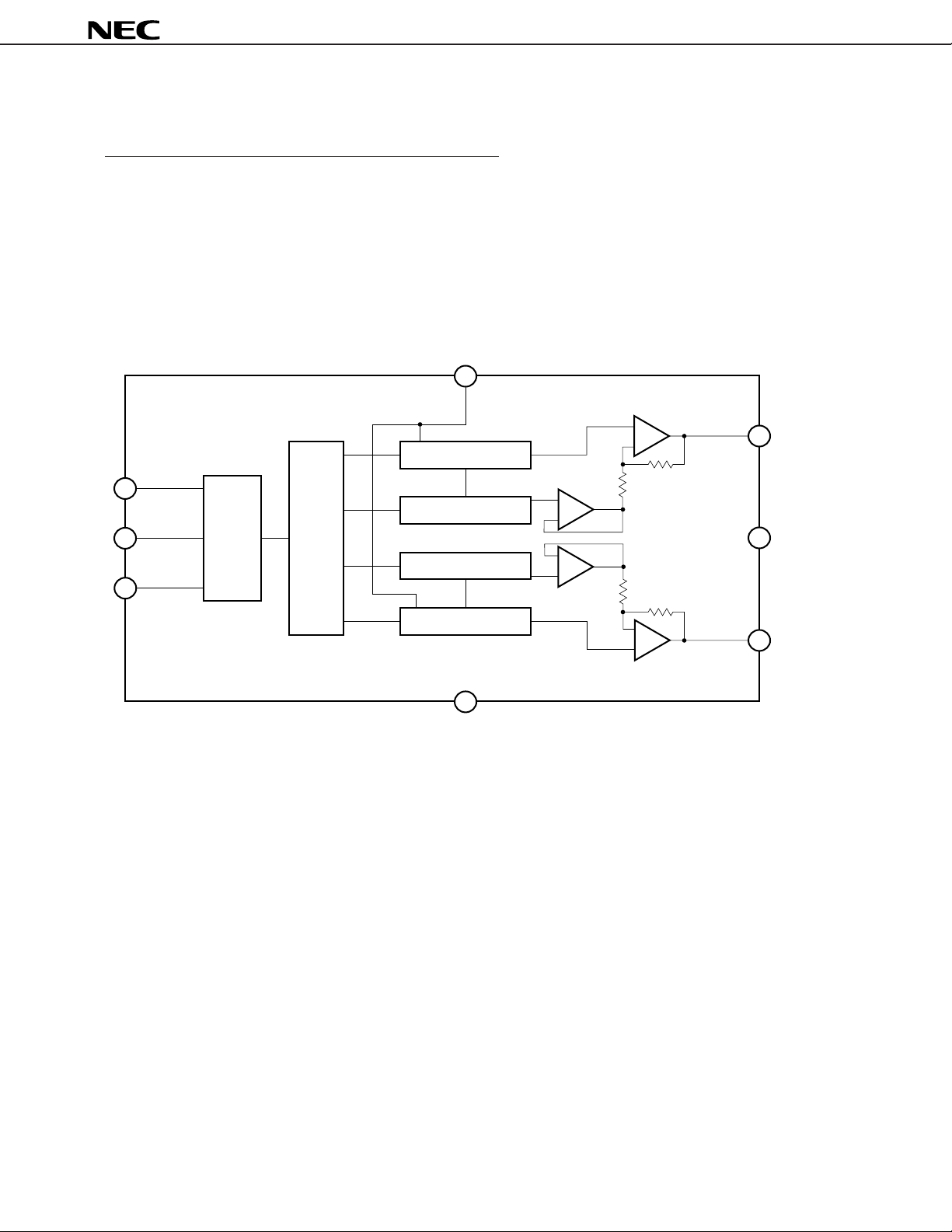
BLOCK DIAGRAM
REF
Main DAC
µ
PD6379, 6379A, 6379L, 6379AL
L. OUT
LRCK
CLK
Sub DAC
GND
Timing
generator
SI
Shift register latch
Sub DAC
Main DAC
V
DD
R. OUT
2
Data Sheet S11588EJ4V0DS00
Page 3
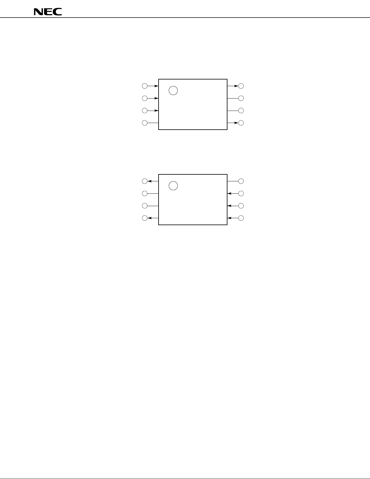
PIN CONFIGURATIONS (Top View)
8-pin plastic SOP (5.72 mm (225))
•µPD6379GR, 6379LGR
µ
PD6379, 6379A, 6379L, 6379AL
LRCK
CLK
V
1
SI
DD
2
3
4
8
7
6
5
L. OUT
GND
REF
R. OUT
•µPD6379AGR, 6379ALGR
R. OUT
REF
GND
L. OUT
1
2
3
4
8
7
6
5
DD
V
CLK
SI
LRCK
Remark The pin configuration of the µPD6379 and 6379L is different from that of the µPD6379A and 6379AL.
Data Sheet S11588EJ4V0DS00
3
Page 4
µ
PD6379, 6379A, 6379L, 6379AL
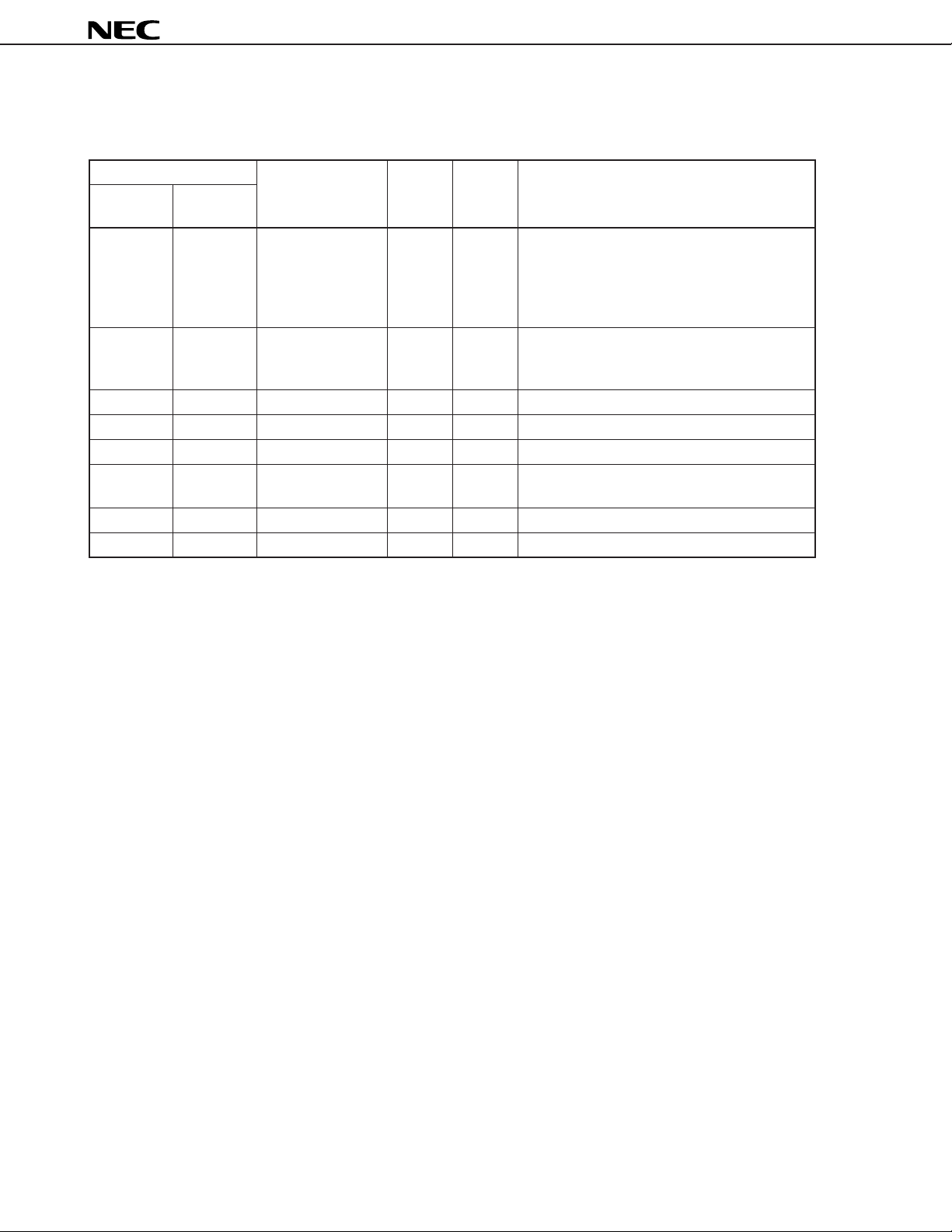
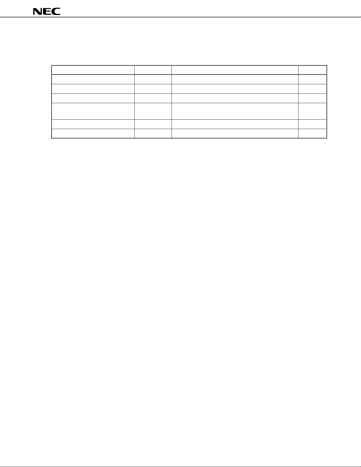
1. PIN FUNCTIONS
Table 1-1 Pin Functions
Pin No.
µ
PD6379,
6379L 6379AL
1 5 Left/Right Clock LRCK Input Input pin to identify left or right input data.
2 6 Serial Input SI Input Serial data input pin.
3 7 Clock CLK Input Serial input data read clock (bit clock) input pin
4 8 Supply Voltage VDD – Positive power supply pin
5 1 R-ch Output R. OUT Output Right analog signal output pin
6 2 Reference Voltage REF – Reference voltage pin. Connect this pin to GND
7 3 Ground GND – GND pin
8 4 L-ch Output L. OUT Output Left analog signal output pin
µ
PD6379A,
Name Symbol I/O Function
µ
PD6379, 6379L: Input “L” to this pin when
inputting L-ch data to SI pin.
µ
PD6379A, 6379AL: Input “H” to this pin
inputting L-ch data to SI pin.
Input data on 2’s complement, MSB first, and
backward justification.
through capacitor.
when
4
Data Sheet S11588EJ4V0DS00
Page 5
µ
PD6379, 6379A, 6379L, 6379AL
2. ELECTRICAL SPECIFICATIONS
ABSOLUTE MAXIMUM RATINGS (TA = 25 °C)
Parameter Symbol Ratings Unit
Supply voltage VDD – 0.3 to +7.0 V
Input voltage VI – 0.3 to VDD + 0.3 V
Output voltage VO – 0.3 to VDD + 0.3 V
Permissible package PD 220 (TA = 75 ˚C) mW
power dissipation
Operating ambient temperature TA –20 to +75 °C
Storage temperature Tstg –40 to +125 °C
Caution Exposure to Absolute Maximum Ratings for extended periods may affect device reliability;
exceeding the ratings could cause permanent damage. The parameters apply independently. The
device should be operated within the limits specified under DC and AC Characteristics.
Data Sheet S11588EJ4V0DS00
5
Page 6

µ
PD6379, 6379A, 6379L, 6379AL
µ
PD6379, 6379A
RECOMMENDED OPERATING CONDITIONS
Parameter Symbol Condition MIN. TYP. MAX. Unit
Supply voltage VDD 4.5 5.0 5.5 V
Logic input voltage (HIGH) VIH 0.7 VDD VDD V
Logic input voltage (LOW) VIL 0 0.3 VDD V
Operating ambient temperature TA –20 +25 +75 °C
Output load resistance RL R. OUT, L. OUT pins 5 kΩ
Conversion frequency fS 200 kHz
Clock frequency fCLK 10 MHz
Clock pulse width tSCK 40 ns
SI, LRCK setup time tDC 12 ns
SI, LRCK hold time tCD 12 ns
ELECTRICAL CHARACTERISTICS (TA = 25 °C, VDD = +5 V, fS = 176.4 kHz)
Parameter Symbol Condition MIN. TYP. MAX. Unit
Resolution RES 16 Bit
Total harmonic distortion THD fIN = 1 kHz, 0 dB 0.04 0.09 %
Full-scale output voltage VFS 2.0 2.3 V p-p
S/N ratio S/N With A-weight filter 93 100 dB
Dynamic range D.R fIN = 1 kHz, –60 dB 89 96 dB
Crosstalk C.T One side channel = 0 dB, fIN = 1 kHz 82 96 dB
Current dissipation IDD fIN = 1 kHz, 0 dB 5 12 mA
6
Data Sheet S11588EJ4V0DS00
Page 7

µ
PD6379, 6379A, 6379L, 6379AL
µ
PD6379L, 6379AL
RECOMMENDED OPERATING CONDITIONS
Parameter Symbol Condition MIN. TYP. MAX. Unit
Supply voltage VDD 3.0 3.3 5.5 V
Logic input voltage (HIGH) VIH 0.7 VDD VDD V
Logic input voltage (LOW) VIL 0 0.3 VDD V
Operating ambient temperature TA –20 +25 +75 °C
Output load resistance RL R. OUT, L. OUT pins 10 kΩ
Conversion frequency fS 200 kHz
Clock frequency fCLK 10 MHz
Clock pulse width tSCK 40 ns
SI, LRCK setup time tDC 12 ns
SI, LRCK hold time tCD 12 ns
ELECTRICAL CHARACTERISTICS (TA = 25 °C, VDD = +3.3 V, fS = 176.4 kHz)
Parameter Symbol Condition MIN. TYP. MAX. Unit
Resolution RES 16 Bit
Total harmonic distortion THD fIN = 1 kHz, 0 dB 0.04 0.09 %
Full-scale output voltage VFS 1.32 1.52 Vp-p
S/N ratio S/N With A-weight filter 93 98 dB
Dynamic range D.R fIN = 1 kHz, –60 dB 89 93 dB
Crosstalk C.T One side channel = 0 dB, fIN = 1 kHz 82 93 dB
Current dissipation IDD fIN = 1 kHz, 0 dB 3 6 mA
Data Sheet S11588EJ4V0DS00
7
Page 8

Timing Chart
CLK
SI
LRCK
( PD6379A,
µ
6379AL)
LRCK
( PD6379,
µ
6379L)
L. OUT
LSB
MSB
1
µ
PD6379, 6379A, 6379L, 6379AL
LSB MSB
2 3 4 5 6 7 8 9 10 11 12 13 14 15 16 1 2 3 4 5 6 7 816
(L-ch)
(L-ch)
N–1
NN
(R-ch)
(R-ch)
9 10 11
R. OUT
CLK
N–1
tSCK tSCK
CLK
tDC tCD
SI
LRCK
tDC
tCD
8
Data Sheet S11588EJ4V0DS00
Page 9

3. APPLICATION CIRCUIT EXAMPLE
µ
PD6379
PD6379A
µ
PD6379L
µ
PD6379AL
Signal processor
LRCKO
SO
BCKO
V
DD
µ
LRCK
SI
CLK
V
DD
+
L.OUT
GND
REF
R.OUT
µ
F47
µ
F0.1
µ
F47
+
µ
PD6379, 6379A, 6379L, 6379AL
V
CC
+
–
1
V
CC
2
+
–
1
V
CC
2
+
L-ch
output
V
CC
+
R-ch
output
Data Sheet S11588EJ4V0DS00
9
Page 10

µ
PD6379, 6379A, 6379L, 6379AL
4. NOTES ON USE
(1) Input signal format
• Input data must be input as 2’s complement, MSB first, and backward justification.
2’s complement is a method of expressing both positive numbers and negative numbers as binary numbers.
See the table below.
2’s Complement Decimal Number L.OUT, R.OUT Pin Voltage TYP. (V)
(Reference Values)
(MSB) (LSB) VDD = 5.0 V VDD = 3.3 V
0111 1111 1111 1111 +32767 3.0 1.98
0111 1111 1111 1110 +32766
0000 0000 0000 0001 +1
0000 0000 0000 0000 0 2.0 1.32
1111 1111 1111 1111 –1
1000 0000 0000 0001 –32767
1000 0000 0000 0000 –32768 1.0 0.66
······
······
······ ······
·················· ··················
Note 1
·················· ··················
Notes 1. Values differ depending on IC fabrication variations, supply voltage fluctuations, and ambient
temperature.
µ
PD6379L, 6379AL
2.
• Make sure that the delimiter of each bit of the data (SI) and the changing timing of LRCK coincide with the
falling edge of CLK.
• It is necessary that 16 clocks be input during 1 sample data period (16 bits). Make sure that the time width
of 1 bit coincides with one cycle of the clock.
• In the input data, the 16 bits preceding the change point of LRCK (shown in “1 sample data period” in Fig.
4-1, and Fig. 4-2) are considered to be valid data and are incorporated for use in D/A conversion.
Note 2
10
Data Sheet S11588EJ4V0DS00
Page 11

µ
16 Invalid Invalid
LSB
CLK
SI 12345678910111213141516 1234
LRCK
MSB LSB MSB
A AB B
1 sample data period
Changing period of LRCK Changing period of LRCK
PD6379, 6379A, 6379L, 6379AL
• If the clock is also supplied to CLK while data is not sampled (refer to Fig. 4-1), make sure that the changing
timing of LRCK coincides with the falling edge (point A) of CLK after the LSB has been input.
Fig. 4-1 Input Timing Chart (1)
CLK
LRCK
A A
LSB
SI
16 Invalid Invalid
MSB LSB MSB
12345678910111213141516 1234
1 sample data period
• If the clock is supplied to CLK only while data is sampled (refer to Fig. 4-2), set the changing timing of LRCK
in between the falling edge (point A) of CLK after the LSB has been input and the start of inputting the next
MSB (point B) (points A and B are included).
Fig. 4-2 Input Timing Chart (2)
Data Sheet S11588EJ4V0DS00
11
Page 12

µ
PD6379, 6379A, 6379L, 6379AL
(2) Output signal updating timing
The L.OUT and R.OUT signals are updated after the input of 3.5 clocks following the change point indicating
the end of the LRCK pin R-ch data input period. Therefore, when the clock is supplied to CLK only during
D/A conversion, the clock must be stopped after the L.OUT and R.OUT signals corresponding to the last input
data are output. Be aware that the L.OUT and R.OUT signals corresponding to the last sample data are not output,
especially when the clock is supplied to CLK only during a sample data period.
Fig. 4-3 Output Timing Chart (1) (for continuous clocks)
3.5 CLK
CLK
SI 123
µ
( PD6379, 6379L)
µ
( PD6379A, 6379AL)
LRCK
LRCK
L.OUT
R.OUT
Fig. 4-4 Output Timing Chart (2) (when there is an interval which the clock is stopped)
CLK
MSB MSB LSB
4 131415
L-ch data (N)
LSB
16 Invalid
CLK stop
123 123
L-ch output (N–1)
R-ch output (N–1)
MSBLSBMSB
4 131415
R-ch data (N)
16 Invalid
LSB
Delay
L-ch output (N)
R-ch output (N)
3.5 CLK
CLK stop
SI
µ
( PD6379, 6379L)
µ
( PD6379A, 6379AL)
LRCK
LRCK
L.OUT
R.OUT
123
4 131415
L-ch data (N) R-ch data (N)
16 Invalid
123 12345
4 131415
L-ch output (N–1)
R-ch output (N–1)
16 Invalid
Delay
(3) Countermeasures against shock noise
It is recommended that a mute circuit be connected to the next stage of the D/A converter. If a mute circuit is
not provided, shock noise may occur when power is applied.
12
Data Sheet S11588EJ4V0DS00
L-ch output
(N)
R-ch output
(N)
Page 13

5. PACKAGE DRAWING
ITEM
B
C
I
8-PIN PLASTIC SOP (5.72 mm (225))
D
E
F
G
H
J
P
MILLIMETERS
1.27 (T.P.)
0.78 MAX.
4.4±0.15
0.1±0.1
0.42
1.59±0.21
6.5±0.3
1.49
+0.08
−0.07
1.1±0.2
3°
+7°
−3°
NOTE
Each lead centerline is located within 0.12 mm of
its true position (T.P.) at maximum material condition.
A 5.2
+0.17
−0.20
K
L
M
N
0.6±0.2
0.17
0.12
0.10
+0.08
−0.07
S8GM-50-225B-6
85
1
4
S
M
C
detail of lead end
A
M
SN
F
G
B
E
D
P
H
I
J
K
L
µ
PD6379, 6379A, 6379L, 6379AL
Data Sheet S11588EJ4V0DS00
13
Page 14

µ
PD6379, 6379A, 6379L, 6379AL
6. RECOMMENDED SOLDERING CONDITIONS
The following conditions must be met for soldering conditions of the product.
For more details, refer to our document “SEMICONDUCTOR DEVICE MOUNTING TECHNOLOGY MANUAL”
(C10535E).
Please consult with our sales offices in case other soldering process is used, or in case the soldering is done under
different conditions.
Table 6-1 Soldering Conditions
µ
PD6379GR, 6379AGR, 6379LGR, 6379ALGR : 8-pin plastic SOP (5.72 mm (225))
Soldering
Process
Infrared ray Peak temperature of package surface: 235 °C or below, IR35-00-2
reflow Reflow time: 30 seconds or less (at 210 °C or higher),
Number of reflow processes: MAX. 2.
VPS Peak temperature of package surface: 215 °C or below, VP15-00-2
Reflow time: 40 seconds or less (at 200 °C or higher),
Number of reflow processes: MAX. 2.
Wave soldering Solder temperature: 260 °C or below, WS60-00-1
Flow time: 10 seconds or less,
Pre-heating temperature: 120 °C or below (Package surface),
Number of flow processes: MAX. 1.
Partial heating Terminal temperature: 300 °C or below, —
method Time: 3 seconds or less (Per one side of the device).
Soldering Conditions Symbol
Caution Do not apply more than one soldering method at any one time, except for “Partial heating
method”.
14
Data Sheet S11588EJ4V0DS00
Page 15

µ
PD6379, 6379A, 6379L, 6379AL
NOTES FOR CMOS DEVICES
1 PRECAUTION AGAINST ESD FOR SEMICONDUCTORS
Note: Strong electric field, when exposed to a MOS device, can cause destruction
of the gate oxide and ultimately degrade the device operation. Steps must
be taken to stop generation of static electricity as much as possible, and
quickly dissipate it once, when it has occurred. Environmental control must
be adequate. When it is dry, humidifier should be used. It is recommended
to avoid using insulators that easily build static electricity. Semiconductor
devices must be stored and transported in an anti-static container, static
shielding bag or conductive material. All test and measurement tools
including work bench and floor should be grounded. The operator should
be grounded using wrist strap. Semiconductor devices must not be touched
with bare hands. Similar precautions need to be taken for PW boards with
semiconductor devices on it.
2 HANDLING OF UNUSED INPUT PINS FOR CMOS
Note: No connection for CMOS device inputs can be cause of malfunction. If no
connection is provided to the input pins, it is possible that an internal input
level may be generated due to noise, etc., hence causing malfunction. CMOS
devices behave differently than Bipolar or NMOS devices. Input levels of
CMOS devices must be fixed high or low by using a pull-up or pull-down
circuitry. Each unused pin should be connected to VDD or GND with a
resistor, if it is considered to have a possibility of being an output pin. All
handling related to the unused pins must be judged device by device and
related specifications governing the devices.
3 STATUS BEFORE INITIALIZATION OF MOS DEVICES
Note: Power-on does not necessarily define initial status of MOS device. Produc-
tion process of MOS does not define the initial operation status of the device.
Immediately after the power source is turned ON, the devices with reset
function have not yet been initialized. Hence, power-on does not guarantee
out-pin levels, I/O settings or contents of registers. Device is not initialized
until the reset signal is received. Reset operation must be executed immediately after power-on for devices having reset function.
Data Sheet S11588EJ4V0DS00
15
Page 16

µ
PD6379, 6379A, 6379L, 6379AL
[MEMO]
• The information in this document is subject to change without notice. Before using this document, please
confirm that this is the latest version.
• No part of this document may be copied or reproduced in any form or by any means without the prior written
consent of NEC Corporation. NEC Corporation assumes no responsibility for any errors which may appear in
this document.
• NEC Corporation does not assume any liability for infringement of patents, copyrights or other intellectual property
rights of third parties by or arising from use of a device described herein or any other liability arising from use
of such device. No license, either express, implied or otherwise, is granted under any patents, copyrights or other
intellectual property rights of NEC Corporation or others.
• Descriptions of circuits, software, and other related information in this document are provided for illustrative
purposes in semiconductor product operation and application examples. The incorporation of these circuits,
software, and information in the design of the customer's equipment shall be done under the full responsibility
of the customer. NEC Corporation assumes no responsibility for any losses incurred by the customer or third
parties arising from the use of these circuits, software, and information.
• While NEC Corporation has been making continuous effort to enhance the reliability of its semiconductor devices,
the possibility of defects cannot be eliminated entirely. To minimize risks of damage or injury to persons or
property arising from a defect in an NEC semiconductor device, customers must incorporate sufficient safety
measures in its design, such as redundancy, fire-containment, and anti-failure features.
• NEC devices are classified into the following three quality grades:
"Standard", "Special", and "Specific". The Specific quality grade applies only to devices developed based on a
customer designated “quality assurance program“ for a specific application. The recommended applications of
a device depend on its quality grade, as indicated below. Customers must check the quality grade of each device
before using it in a particular application.
Standard: Computers, office equipment, communications equipment, test and measurement equipment,
audio and visual equipment, home electronic appliances, machine tools, personal electronic
equipment and industrial robots
Special: Transportation equipment (automobiles, trains, ships, etc.), traffic control systems, anti-disaster
systems, anti-crime systems, safety equipment and medical equipment (not specifically designed
for life support)
Specific: Aircraft, aerospace equipment, submersible repeaters, nuclear reactor control systems, life
support systems or medical equipment for life support, etc.
The quality grade of NEC devices is "Standard" unless otherwise specified in NEC's Data Sheets or Data Books.
If customers intend to use NEC devices for applications other than those specified for Standard quality grade,
they should contact an NEC sales representative in advance.
M7 98.8
 Loading...