

Page 1
DATA SHEET
MOS INTEGRATED CIRCUIT
µ
PD4990A
SERIAL I/O CALENDAR & CLOCK
CMOS LSI
The µPD4990A is a CMOS LSI developed to input/output calendar & clock data serially to/from the micro computer.
The crystal frequency is 32.768 kHz and the data items included are time, minute, second, year, month, day, and
week.
FEATURES
Built-in counters for time (hour, minute, and second) and date (year, month, day, and week)
•
Leap years are adjusted automatically.
•
Data is represented in BCD notation (except months in hexadecimal notation) and input/output serially.
•
Commands can be set by inputting serial data.
•
Selective timing pulses (TPs) are 64 Hz, 256 Hz, 2 048 Hz, and 4 096 Hz and selective output intervals are 1, 10,
•
30, and 60 seconds.
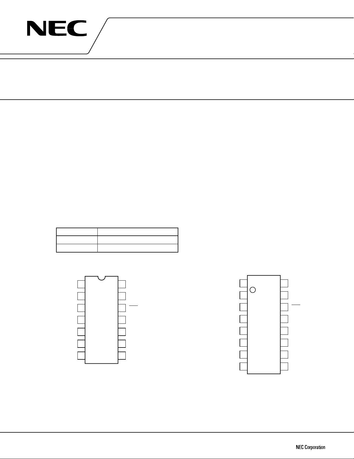
ORDERING INFORMATION
PART No. PACKAGE
µ
PD4990AC 14-pin plastic DIP (300 mil)
µ
PD4990AG 16-pin plastic SOP (300 mil)
CONNECTION DIAGRAM (Top View)
114
C
2
C
1
C
0
STB
CS
DATA IN
GND
(V
SS
)
213
312
411
510
69
7
PD4990AC
µ
V
X
X
OUT ENBL
TP
DATA OUT
CLK
8
DD
TAL
TAL
(+)
C
2
C
1
C
0
NC
STB
CS
DATA IN
GND
(V
SS
)
NC: NO CONNECTION
116
215
314
413
512
611
7
89
PD4990AG
µ
10
DD
(+)
V
X
TAL
X
TAL
NC
OUT ENBL
TP
DATA OUT
CLK
Document No. IC-1755 (1st edition)
Date Published March 1997 P
Printed in Japan
©
1989
Page 2
µ
PD4990A
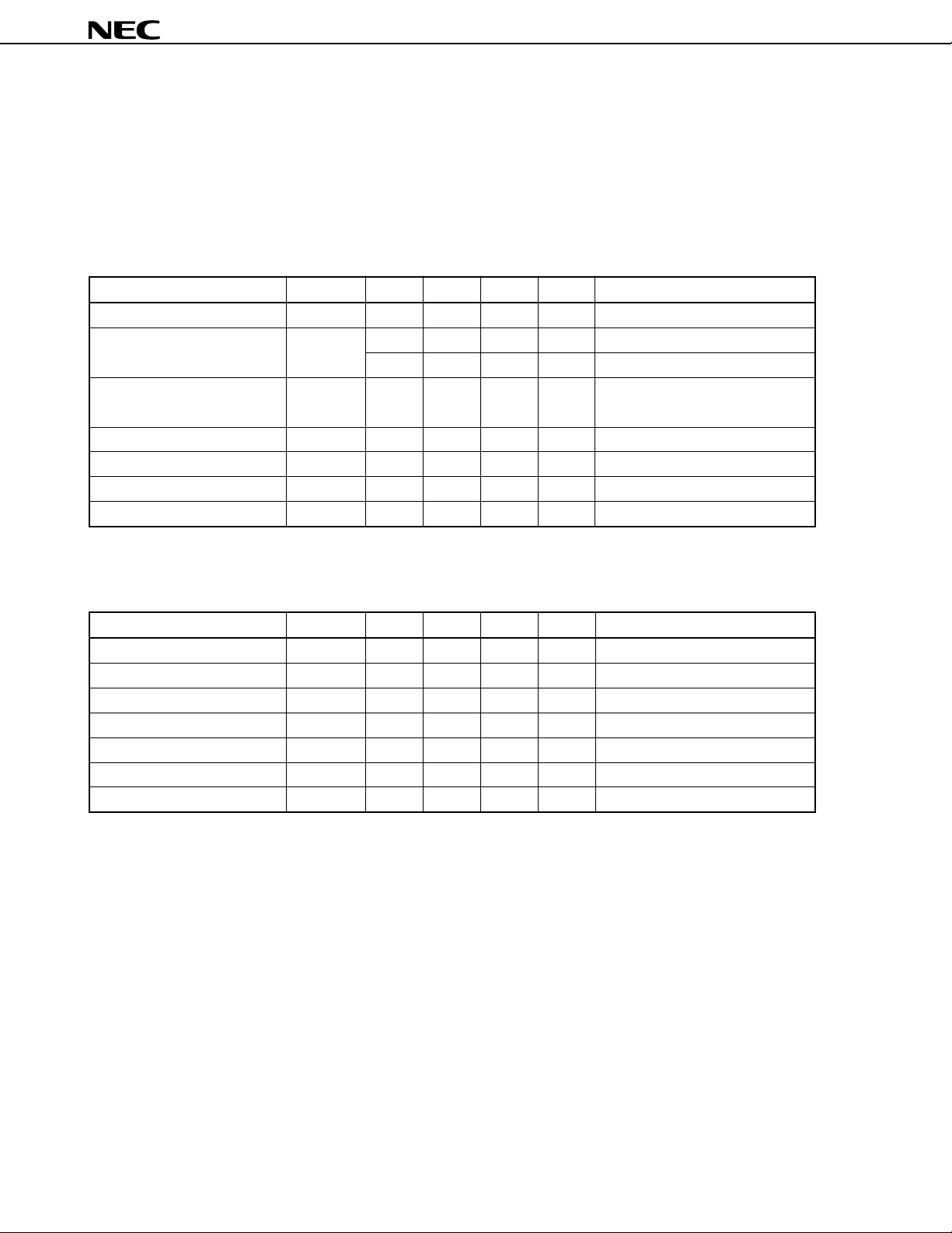
ABSOLUTE MAXIMUM RATINGS
Supply Voltage VDD − VSS −0.5 to 7.0 V
Input Voltage V
Operating Temperature Range T
Storage Temperature Range T
Output Terminal Voltage V
IN VSS −0.3 to VDD +0.3 V
opt −40 to +85 °C
stg −65 to +125 °C
OUT −0.5 to 7.0 V
ELECTRICAL CHARACTERISTICS (f = 32.768 kHz, CG = CD = 20 pF, CI = 20 kΩ, Ta = 25 °C)
CHARACTERISTIC SYMBOL MIN. TYP. MAX. UNIT TEST CONDITIONS
Operating Voltage VDD − VSS 2.00 5.50 V
Current Consumption IDD
Low Level Output Voltage V OL 0.4* V
CLK Input Frequency fCLK DC 500 kHz VDD − VSS = 2.0 V, Duty 50 %
Input Leakage Current IIN ±1
High Level Input Voltage VIH 0.7 VDD VDD V
Low Level Input Voltage VIL VSS 0.3 VDD V
820
100
µ
AVDD − VSS = 3.60 V
µ
AVDD − VSS = 5.50 V
VDD − VSS = 2.0 to 5.5 V
IOL = 500 µA
µ
AVDD − VSS = 5.50 V
* TP and DATA OUT are N-channel open drain output.
A.C. ELECTRICAL CHARACTERISTICS (f = 32.768 kHz, VDD − VSS = 2.0 V, Ta = 25 °C)
CHARACTERISTIC SYMBOL MIN. TYP. MAX. UNIT TEST CONDITIONS
C0 to 2, CS − STB Set-up Time tSU 1
STB Pulse Width tSTB 1
C0 to 2, CS − STB Hold Time tHLD 1
STB LATCH Delay Time td1 1**
CLK-DATA OUT Delay time td(c-o) 1
DATA IN Set-up Time tDSU 1
DATA IN Hold Time tDHLD 1
** Note: When a function mode is Time Read mode (other than Test mode), STB LATCH delay time is 20 µs MAX.
d2).
(t
µ
s
µ
s
µ
s
µ
s except Time Read mode
µ
sRL = 33 kΩ, CL = 15 pF
µ
s
µ
s
2
Page 3
OE
BLOCK DIAGRAM
CLK
DATA
IN
X
TAL
X
TAL
C
C
C
CS
STB
CLK
COMMAND
Register
48 Bit Shift Register
MPX
OPEN DRAIN
DATA
OUT
CLK RH
N-ch
CS
3'C2'C1'C0
'
PS
MON
-TH
D/W
HOUR MINYEAR DAY SEC
1 Hz
C
Time counter
15 Stage Binary Divider
15
OSC
1/2
Select signal
generator circuit
64 Hz
STOP
C3'
2
'
C
C
1
'
C
0
'
2
1
0
DATA SELECTOR
DECODER
TEST
1/2
1 Hz
6
SEC
RESET
TP
MPX
MPX
:
Multiplexer
PS
:
D/W
CS
TP
RH
Preset
:
Day of the Week
:
Chip Select
:
Timing Pulse
:
Register Hold
µ
PD4990A
3
Page 4
FUNCTION SPECIFICATIONS
Crystal frequency (X tal osc.).
•
32.768 kHz
°
Data
•
Data types are: second, minute, day, week, month, and year.
Leap years, 31-day months, and months with 30 or less days are adjusted automatically.
A 24-hour system is used and last two digits of Gregorian year are indicated.
It is assumed that leap years are expressed by multiples of 4.
Data format
•
Data is represented in BCD notation. Only months are represented in hexadecimal notation.
Data input-output and Clock
•
Data is input/output synchronously with reference to the external clocks input from the CLK pin using the serial
input/output system. (See Fig. 1.)
Timing pulse output
•
Three frequencies, 64 Hz, 256 Hz, and 2 048 Hz, can be set with C
Using serial data input command, selective timing pulses (TPs) are 64 Hz, 256 Hz, 2 048 Hz, and 4 096 Hz
and selective output intervals are 1, 10, 30, and 60 seconds.
0, C1 and C2 pins.
µ
PD4990A
Function mode selection
•
A function mode can be selected by the inputs from C
serial data input. (C
0 = C1 = C2 = VDD)
0, C1, and C2. Also a function mode can be selected through
Each command is latched with STB (strobe).
Chip select
•
Connecting the CS pin to the ground level inhibits CLK and STB inputs.
Data output inhibition
•
Connecting the OUT ENBL pin to the ground level sets the DATA OUT pin at high impedance.
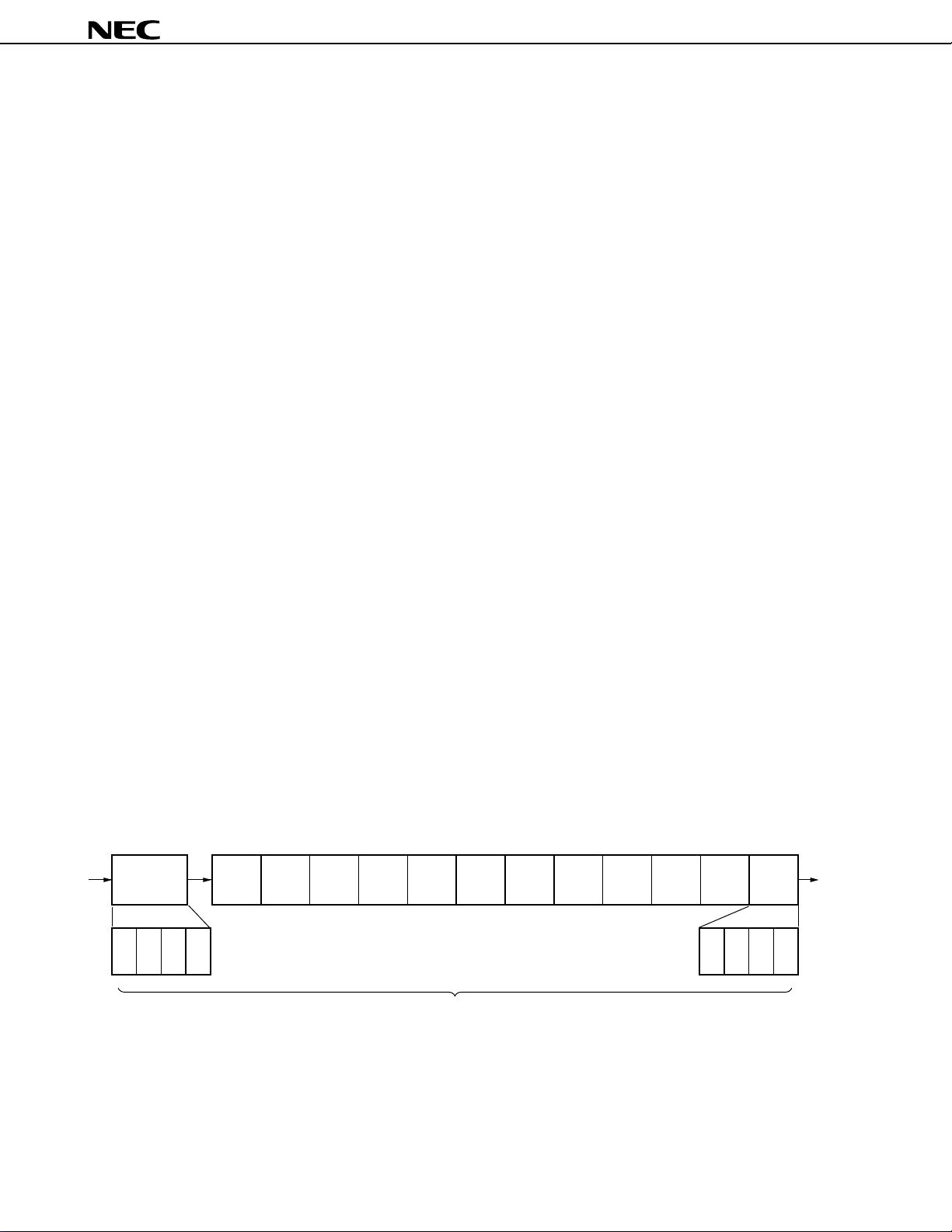
Figure 1.
command
register
C
3
'
C2'C1'C0' D3D2D1D
Ten's of
* DATA of 52 Bit Shift Register appears on DATA OUT terminal from LSB of second.
year
Unit of
year
month
day of
the week
Ten's of
days
52 Bit Shift Register
Unit of
days
Ten's of
hours
Unit of
hours
Ten's of
minutes
Unit of
minutes
Ten's of
seconds
LSBMSB
Unit of
seconds
0
4
Page 5

TERMINALS
Input terminals
•
DATA IN Data input of 40-/52-bit shift register
°
CLK Shift clock input of 40-/52-bit shift register
°
C0, C1, C2 Command input (3 bit)
°
STB Strobe input
°
CS Chip select input (Prohibits CLK & STB)
°
OUT ENBL Output control input (Makes the DATA OUT high impedance by inputting low level).
°
Output terminals (N-channel Open Drain)
•
DATA OUT Data output of 40-/52-bit shift register
°
TP Timing pulse output
°
Oscillation terminals
•
XTAL Oscillation inverter input (OSC IN)
°
XTAL Oscillation inverter output (OSC OUT)
°
Power supply terminals
•
VDD Plus power supply
°
GND (VSS) Common line
°
µ
PD4990A
5
Page 6
COMMAND SPECIFICATIONS
Commands input from C0, C1, and C2 pins (1 ...H, 0 ...L)
°
Shift register 40 bit (The year function is ineffective.)
µ
(Operates as the existing
C2 C1 C0 FUNCTION
0 0 0 Register Hold DATA OUT = 1 Hz
0 0 1 Register Shift DATA OUT = [LSB] = 0 or 1
0 1 0 Time Set & Counter Hold DATA OUT = [LSB] = 0 or 1
0 1 1 Time Read DATA OUT = 1 Hz
1 0 0 TP = 64 Hz
1 0 1 TP = 256 Hz
1 1 0 TP = 2 048 Hz
1 1 1 Serial command transfer mode
* The test mode is cancelled by [C2, C1, C0] = [0, 0, 0] to [1, 1, 0].
Serial data commands
°
2, C1, C0] = [1, 1, 1] at all time.
Set [C
Shift register 52 bit (The year function is effective.)
PD1990AC in other than test mode)
µ
PD4990A
C3'C2'C1'C0' FUNCTION
0 0 0 0 Register Hold DATA OUT = 1 Hz
0 0 0 1 Register Shift DATA OUT = [LSB] = 0 or 1
0 0 1 0 Time Set & Counter Hold DATA OUT = [LSB] = 0 or 1
0 0 1 1 Time Read DATA OUT = 1 Hz
0 1 0 0 TP = 64 Hz
0 1 0 1 TP = 256 Hz
0 1 1 0 TP = 2 048 Hz
0 1 1 1 TP = 4 096 Hz
1 0 0 0 TP = 1 s interval set (counter reset & start)
1 0 0 1 TP = 10 s interval set (counter reset & start)
1 0 1 0 TP = 30 s interval set (counter reset & start)
1 0 1 1 TP = 60 s interval set (counter reset & start)
1 1 0 0 Interval Output Flag Reset
1 1 0 1 Interval Timer Clock Run
1 1 1 0 Interval Timer Clock Stop
1 1 1 1 TEST MODE SET
When serial data commands are used, C0, C1, and C2 pins should be connected VDD pin.
6
Page 7

Command input
•
(1) 3-bit binary code input: C
(2) 4-bit serial transfer command input: C3', C2', C1', C0'
Number of commands
•
Commands (C3', C2', C1', C0' commands are made effective only when [C2, C1, C0] = [1, 1, 1].)
•
(1) Register control [C
Register Hold Mode [0, 0, 0] / [0, 0, 0, 0]
°
[C
2, C1, C0]
The 40-bit shift register is held. The year function is ineffective.
3', C2', C1', C0']
[C
The 48-bit shift register is held.
The command register is not held.
* The DATA OUT output frequency is 1 Hz.
Register Shift Mode [0, 0, 1] / [0, 0, 0, 1]
°
2, C1, C0]
[C
The 40-bit shift register data can be shifted. The year function is ineffective.
[C3', C2', C1', C0']
Data in 52-bit shift registers (including command registers) can be shifted. For command register, data can
be always shifted using the serial command transfer mode.
* The DATA OUT output is LSB data from the shift register.
Time Set and Counter Hold Mode [0, 1, 0] / [0, 0, 1, 0]
°
2, C1, C0]
[C
Data is transferred from the 40-bit shift register to the time counter. The year function is ineffective.
[C3', C2', C1', C0']
Data is transferred from the 48-bit shift register to the time counter.
* This command is used to reset the last 10-15 of 15 Stage Binary Divider and holds the time counter.
15 Stage Binary Divider resetting and time counter release are executed by the following:
[C2, C1, C0] = [0, 0, 0] [0, 0, 1] [0, 1, 1] [C3', C2', C1', C0'] = [0, 0, 0, 0] [0, 0, 0, 1] [0, 0, 1, 1]
The time setting accuracy is ±15.625 ms.
The DATA OUT pin outputs LSB data (0 or 1) from the shift register.
After this command is executed, the 40-/48-bit shift register is held and data cannot be shifted.
Time Read Mode [0, 1, 1] / [0, 0, 1, 1]
°
2, C1, C0]
[C
Data is transferred from the time-counter to the 40-bit shift register. The year function is ineffective.
[C3', C2', C1', C0']
Data is transferred from the time counter to the 48-bit shift register.
* The DATA OUT pin output is a 1 Hz frequency.
After this command is executed, the 40-/48-bit shift register is held and data cannot be shifted.
2, C1, C0
C2, C1, C0 C'3, C'2, C'1, C'0
Register control 4 4
TP select 3 8
TP control 0 3
Test mode set 1 1
2, C1, C0] / [C3', C2', C1', C0']
µ
PD4990A
7
Page 8

(2) TP selection and control [C2, C1, C0] / [C3', C2', C1', C0']
TP = 64 Hz Set Mode [1, 0, 0] / [0, 1, 0, 0]
•
64 Hz (50 % duty) is output to the TP pin.
2, C1, C0]: The year function is ineffective and the interval timer stops.
[C
TP = 256 Hz Set Mode [1, 0, 1] / [0, 1, 0, 1]
•
256 Hz (50 % duty) is output to the TP pin.
2, C1, C0]: The year function is ineffective and the interval timer stops.
[C
TP = 2 048 Hz Set Mode [1, 1, 0] / [0, 1, 1, 0]
•
2 048 Hz (50 % duty) is output to the TP pin.
2, C1, C0]: The year function is ineffective and the interval timer stops.
[C
Modes permitted only for serial commands [C
TP = 4 098 Hz Set Mode [0, 1, 1, 1]
•
4 098 Hz (50 % duty) is output to the TP pin. The interval timer stops.
TP = 1-second Interval Set Mode (counter reset & start) [1, 0, 0, 0]
•
A 1-second interval signal is output to the TP pin.
TP = 10-second Interval Set Mode (counter reset & start) [1, 0, 0, 1]
•
A 10-second interval signal is output to the TP pin.
TP = 30-second Interval Set Mode (counter reset & start) [1, 0, 1, 0]
•
A 30-second interval signal is output to the TP pin.
TP = 60-second Interval Set Mode (counter reset & start) [1, 0, 1, 1]
•
A 60-second interval signal is output to the TP pin.
Interval Output Flag Reset [1, 1, 0, 0]
•
The interval signal output to the TP pin is reset.
The interval timer counter continue the operation.
Interval Timer Clock Run [1, 1, 0, 1]
•
The timer for outputting interval signals is reset then started.
Interval Timer Clock Stop [1, 1, 1, 0]
•
The timer for outputting interval signals stops.
The output status does not change.
3', C2', C1', C0']
µ
PD4990A
(3) Serial command transfer mode setting
Set [C
2, C1, C0] = [1, 1, 1]
(4) Test mode setting
Set [C
2, C1, C0] = [1, 1, 1] [C3', C2', C1', C0'] = [1, 1, 1, 1]
3-bit parallel command setting mode [C2, C1, C0]
°
The year function is ineffective when commands are input through C
Generally, February involves 28 days. The 29th day can be set optionally. The next day of the February
29th can be set the March 1st automatically. The interval timer is in the halt state.
* The test mode is cancelled by [C
Serial command transfer mode [C3', C2', C1', C0']
°
If a strobe signal is input with C
command register ([C
* The test mode is cancelled by [C
= [0, 0, 0]
= [0, 1, 0, 0] to [1, 1, 1, 0]
In this mode, the serial command register is not held with the Register Hold command. Accordingly, the serial
command can be executed irrespective of the mode if the CS pin is active.
The year function is effective in the serial command transfer mode.
3', C2', C1', C0']) are received as a command; the year function is effective.
8
2, C1, and C0 pins.
2, C1, C0] = [0, 0, 0] to [1, 1, 0].
2, C1, and C0 pins set at the VDD level ([1, 1, 1]), the contents of the serial
3', C2', C1', C0']
Page 9

µ
PD4990A
Interval output function
°
An interrupt signal can be output by selecting an output from TP.
Interrupt signals are output repeatedly at specified intervals until their output is suppressed by a command.
Only output flags can be reset to operate the timer continuously.
0.5 s
1 s 1 s
Interval Output
Flag Reset
Interval of 1 second
The interval signal waveform is rectangular (50 % duty) if not reset.
The interval timer is independent of the Timer Counter, so it is not affected by the resetting of the current
time timer.
30 s
60 s
The interval timer accuracy is ±15.625 ms.
* The interval timer counter is reset by [1, 0, 0, 0] through [1, 0, 1, 1].
1 s
Interval Timer
Clock Stop
Interval Output
Flag Reset
9
Page 10

µ
PD4990A
Test mode
°
In the test mode, data is output to the DATA OUT pin regardless of whether data has been input to OUT
ENBL.
There are two different test modes depending on the OUT ENBL data.
(1) Test mode 1 (OUT ENBL = 0)
8 192 Hz signals are set parallel in the counters for year, month, week, day, time, minute, and second.
There is no carry from these counters.
Year
counter
8 192 Hz
Month
counter
Week
counter
Day
counter
Time
counter
Minute
counter
Second
counter
(2) Test mode 2 (OUT ENBL = 1)
A 8 192 Hz signal is input to the second counter instead of the 1 Hz signal. There is carry from counters.
8 192 Hz
Year
counter
Month
counter
Week
counter
Day
counter
Time
counter
Minute
counter
Second
counter
Outputs from DATA OUT and TP OUT pins in different function modes are listed below.
MODE DATA OUT TP Others
REGISTER HOLD 1 Hz 64 Hz By this command, TEST MODE is released.
REGISTER SHIFT LSB of shift register 32 Hz 8 192 Hz input to time counter
TIME SET LSB of shift register L Level Test mode
TIME READ 1 Hz 32 Hz 8 192 Hz input to time counter
10
When the REGISTER HOLD command cancels the test mode, 64 Hz is output to the TP pin.
Page 11

TIMING DIAGRAM FOR SETTING COMMANDS (C0', C1', C2', C3')
Figure 2.
V
DATA
IN
V
IH
IL
V
t
DSU
C0'
C
1
'C
t
DHLD
2
'C
3
'
IH
V
IL
µ
PD4990A
CLK
STB
NEW COMMAND
VALID
VDD − VSS = 2.0 V tDSU = 1 µs MIN.
IH
V
V
IL
Other than time read mode
OLD MODE
Time read mode
OLD MODE
DHLD = 1
t
HLD = 1
t
t
STB = 1
d1 = 1
t
d2 = 20
t
V
IH
V
IL
t
HLD
V
IH
V
IL
µ
s MIN.
µ
s MIN.
µ
s MIN.
µ
s MAX. (Other than time read mode)
µ
s MAX. (Time read mode)
t
STB
t
d1
NEW MODE
t
d2
NEW MODE
Note: Command (C2, C1, C0) is set to (1, 1, 1)
CS = "H"
A mode is latched by STB and held until another mode in the same group is set.
11
Page 12

TIMING DIAGRAM FOR SETTING COMMANDS (C0, C1, C2)
Figure 3.
V
C2,C1,C
CS
STB
0
IH
IL
V
t
SU
V
IH
t
SU
t
STB
V
IH
V
IL
t
S-C
t
HLD
t
HLD
t
S-C
µ
PD4990A
CAN CHANGECAN CHANGE STABLE
IH
V
V
IL
V
IH
CLK
V
IL
Other than time read mode
t
NEW COMMAND
VALID
OLD MODE
d1
NEW MODE
Time read mode
t
d2
OLD MODE
V
DD − VSS = 2.0 V tSU = 1
t
HLD = 1
STB = 1
t
d1 = 1
t
t
d2 = 20
S-C = 1
t
µ
s MIN.
µ
s MIN.
µ
s MIN.
µ
s MAX. (Other than time read mode)
µ
s MAX. (Time read mode)
µ
s MIN.
NEW MODE
Note: A mode is latched by STB and held until another mode in the same group is set.
12
Page 13

DATA INPUT/OUTPUT TIMING DIAGRAM
Command (C2, C1, C0) is set to (1, 1, 1).
Command (C3', C2', C0') is set to [0001] (Register Shift Mode).
CS = "H"
CLK
DATA
IN
OUT
ENBL
DATA
OUT
01234567891011 4041424344454647
Note: Reading-in timing of CPU (Trailing edge of CLK).
Figure 4.
"1" year "10" year"1" s. "1" min."10" s.
"1" year "10" year"1" s. "1" min."10" s.
'70
July 16 (Sun.)
2 hours 24 minutes
35 seconds.
'86
November 25 (Sat.)
2 hours 23 minutes
49 seconds.
Written-in data LSB ("H")
appears at output.
µ
PD4990A
INPUT
TIMING
OUTPUT
TIMING
TIMING DIAGRAM OF DATA INPUT AND OUTPUT
Figure 5.
V
IH
CLK
DATA OUT
DATA IN
t
DSU
V
IH
IL
V
t
dC-O
:
1 s MAX. (RL = 33 kΩ, CL = 25 pF)
µ
t
DSU
t
DHLD
µ
:
1 s MIN.
µ
:
1 s MIN.
V
IL
t
dC-O
t
V
OH
V
OL
DHLD
13
Page 14

POWER SUPPLY CIRCUIT
1SS53
+5 V
15 kΩ
4.7 kΩ
2SA733
1 kΩ
510 Ω
2SC945
1SS53
3.6 V
Ni−Cd
DD
V
C
0
C
1
C
2
µ
PD4990A
CS
OE
DIN
CLK
STB
Power
Fail
µ
PD4990A
10 kΩ
GND
V
SS
TP D
X
X
OUT
TAL
TAL
32.768 kHz
G
= 20 pF
C
C
D
= 5 to 30 pF
+5 V
10 kΩ
14
Page 15

APPLICATION
+5 V
10 kΩ
DATA BUS
WR
µ
PD4990A
D
7
D
6
D
5
D
4
D
3
D
2
D
1
D
0
Power Fail
12
13
4
D
5
D
D
D
9
CLK
µ
0
Q
1
Q
2
Q
3
Q
RESET
PD4175BC
Power Supply
Circuit
0
1
2
3
2
7
10
15
1
RESET of
SYSTEM
CS
DIN
CLK
STB
V
DD
C
0
1
C
C
2
µ
PD4990A
D
OUT
OE
RD
Address Decoder
+5 V
10 kΩ
TP
INT
32.768 kHz
C
G
= 20 pF
X
TAL
TAL
X
C
D
= 5 to 30 pF
15
Page 16

14PIN PLASTIC DIP (300 mil)
14 8
17
A
I
J
µ
PD4990A
K
L
H
G
NOTES
1) Each lead centerline is located within 0.25 mm (0.01 inch) of
its true position (T.P.) at maximum material condition.
2) Item "K" to center of leads when formed parallel.
F
M
D
N
C
B
M
ITEM MILLIMETERS INCHES
A
20.32 MAX.
B 2.54 MAX.
C 2.54 (T.P.) 0.100 (T.P.)
D 0.50±0.10 0.020
F 1.2 MIN. 0.047 MIN.
G
3.5±0.3
H 0.51 MIN.
I 4.31 MAX.
J
5.08 MAX.
K 7.62 (T.P.)
L 6.4
M 0.25 0.010
N
R 0~15°
+0.10
–0.05
0.25 0.01
R
0.800 MAX.
0.100 MAX.
+0.004
–0.005
0.138±0.012
0.020 MIN.
0.170 MAX.
0.200 MAX.
0.300 (T.P.)
0.252
+0.004
–0.003
0~15°
P14C-100-300A,C-1
16
Page 17

16 PIN PLASTIC SOP (300 mil)
ITEM MILLIMETERS INCHES
A
B
C
E
F
G
H
I
J
10.46 MAX.
1.27 (T.P.)
1.8 MAX.
1.55
7.7±0.3
0.78 MAX.
0.12
1.1
5.6
M
0.1±0.1
N
0.412 MAX.
0.031 MAX.
0.004±0.004
0.071 MAX.
0.061
0.303±0.012
0.220
0.043
0.005
0.050 (T.P.)
P16GM-50-300B-4
P 3 ° 3°
+7°
NOTE
Each lead centerline is located within 0.12 mm (0.005 inch) of
its true position (T.P.) at maximum material condition.
D 0.40 0.016
+0.10
–0.05
K 0.20 0.008
+0.10
–0.05
L 0.6±0.2 0.024
0.10
–3°
+7°
–3°
0.004
+0.008
–0.009
+0.004
–0.002
+0.004
–0.003
A
C
D
G
P
detail of lead end
F
E
B
H
I
L
K
M
M
1 8
916
J
N
µ
PD4990A
17
Page 18

[MEMO]
µ
PD4990A
18
Page 19

[MEMO]
µ
PD4990A
19
Page 20

µ
PD4990A
No part of this document may be copied or reproduced in any form or by any means without the prior written
consent of NEC Corporation. NEC Corporation assumes no responsibility for any errors which may appear in
this document.
NEC Corporation does not assume any liability for infringement of patents, copyrights or other intellectual property
rights of third parties by or arising from use of a device described herein or any other liability arising from use
of such device. No license, either express, implied or otherwise, is granted under any patents, copyrights or other
intellectual property rights of NEC Corporation or others.
While NEC Corporation has been making continuous effort to enhance the reliability of its semiconductor devices,
the possibility of defects cannot be eliminated entirely. To minimize risks of damage or injury to persons or
property arising from a defect in an NEC semiconductor device, customers must incorporate sufficient safety
measures in its design, such as redundancy, fire-containment, and anti-failure features.
NEC devices are classified into the following three quality grades:
"Standard", "Special", and "Specific". The Specific quality grade applies only to devices developed based on a
customer designated "quality assurance program" for a specific application. The recommended applications of
a device depend on its quality grade, as indicated below. Customers must check the quality grade of each device
before using it in a particular application.
Standard: Computers, office equipment, communications equipment, test and measurement equipment,
audio and visual equipment, home electronic appliances, machine tools, personal electronic
equipment and industrial robots
Special: Transportation equipment (automobiles, trains, ships, etc.), traffic control systems, anti-disaster
systems, anti-crime systems, safety equipment and medical equipment (not specifically designed
for life support)
Specific: Aircrafts, aerospace equipment, submersible repeaters, nuclear reactor control systems, life
support systems or medical equipment for life support, etc.
The quality grade of NEC devices is "Standard" unless otherwise specified in NEC's Data Sheets or Data Books.
If customers intend to use NEC devices for applications other than those specified for Standard quality grade,
they should contact an NEC sales representative in advance.
Anti-radioactive design is not implemented in this product.
M4 96.5
 Loading...