

Page 1
DATA SHEET
BIPOLAR DIGITAL INTEGRATED CIRCUIT
µµµµ
PB1508GV
3 GHz INPUT DIVIDE BY 2 PRESCALER IC
FOR DBS TUNERS
PB1508GV is a 3.0 GHz input divide by 2 prescaler IC for DBS tuner applications. µPB1508GV can make
µ
VHF/UHF band PLL frequency synthesizer apply to DBS/ECS tuners. µPB1508GV is a shrink package version of
PB584G so that this small package contributes to reduce the mounting space.
µ
PB1508GV is manufactured using NEC’s high fT NESAT™ IV silicon bipolar process. This process uses silicon
µ
nitride passivation film and gold electrodes. These materials can protect chip surface from external pollution and
prevent corrosion/migration. Thus, this IC has excellent performance, uniformity and reliability.
FEATURES
• High toggle frequency : fin = 0.5 GHz to 3.0 GHz
• High-density surface mounting : 8 pin plastic SSOP (175 mil)
• Low current consumption : 5 V, 12 mA
• Fixed division :÷2
APPLICATION
• Prescaler between local oscillator and PLL frequency synthesizer included modulus prescaler
• DBS tuners with kit use of VHF/UHF band PLL frequency synthesizer
ORDERING INFORMATION
PART NUMBER PACKAGE MARKING SUPPLYING FORM
µ
PB1508GV-E1 8 pin plastic SSOP
(175 mil)
Remarks
To order evaluation samples, please contact your local NEC sales office.
(Part number for sample order:
µ
1508 Embossed tape 8 mm wide. Pin 1 is in tape pull-out
direction. 1 000 p/reel.
PB1508GV)
Document No. P10768EJ2V0DS00 (2nd edition)
Date Published September 1997 N
Printed in Japan
Caution: Electro-static sensitive devices
1996©
Page 2
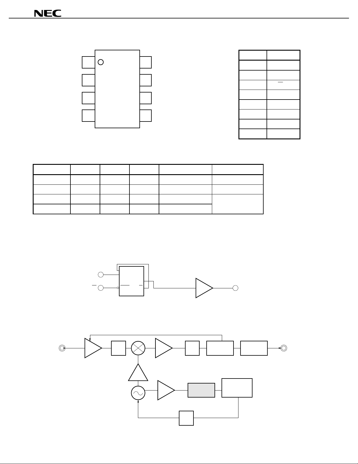
PIN CONNECTION (Top View)
1
2
3
4
PRODUCT LINE-UP
Product No. ICC (mA) fin (GHz) VCC (V) Package Pin Connection
PB581A 30 0.5 to 2.8 4.5 to 5.5 8 pins CAN –
µ
PB581C 30 0.5 to 2.2 4.5 to 5.5 8 pins DIP (300 mil) NEC Original
µ
PB584G 18 0.5 to 2.5 4.5 to 5.5 8 pins SOP (225 mil) NEC Original
µ
PB1508GV 12 0.5 to 3.0 4.5 to 5.5 8 pins SSOP (175 mil)
µ
8
7
6
5
µµµµ
PB1508GV
Pin No. Pin name
1V
2IN
3IN
4 GND
5 GND
6NC
7 OUT
8NC
CC
Remarks
This table shows the TYP values of main parameters. Please refer to ELECTRICAL
CHARACTERISTICS.
PB581A, µPB581C and µPB584G are discontinued.
µ
INTERNAL BLOCK DIAGRAM
IN
IN
SYSTEM APPLICATION EXAMPLE
RF unit block of DBS tuners
1stIF input
from DBS converter
BPF
D
CLK
CLK
OSC
MIX
Q
Q
AMP
SAW AGC amp. FM demo.
PB1508GV
µ
÷ 2
Prescaler
OUT
Baseband output
PLLsynth.
for VHF/UHF
band
LPF
2
Page 3
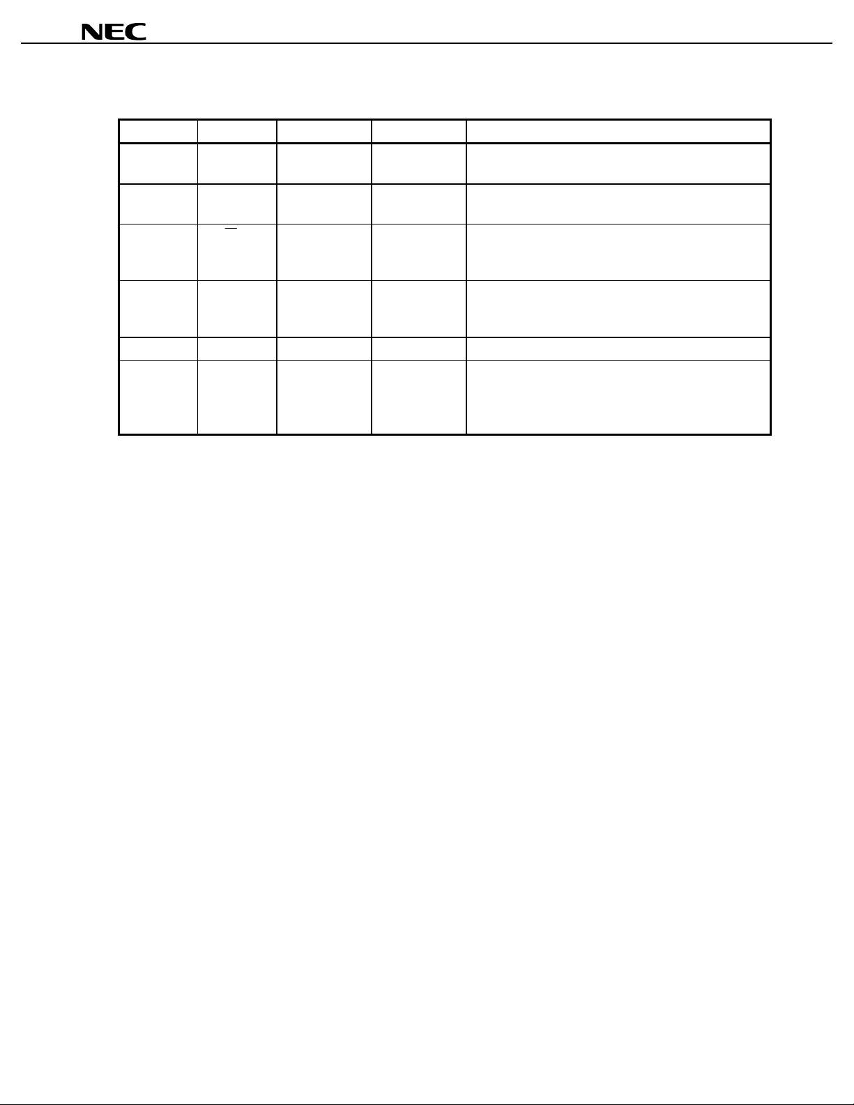
PIN EXPLANATION
Pin No. Symbol Applied voltage PIN voltage Functions and explanation
µµµµ
PB1508GV
1VCC4.5 to 5.5
2IN
3IN
4, 5 GND 0
6, 8 NC
7 OUT
1.7 to 4.95 Signal input pin. This pin should be coupled to signal
1.7 to 4.95 Signal input bypass pin. This pin must be equipped with
1.0 to 4.7 Divided frequency output pin. This pin is designed as
Power supply pin. This pin must be equipped with bypass
capacitor (eg 1 000 pF) to minimize ground impedance.
source with capacitor (eg 1 000 pF) for DC cut.
bypass capacitor (eg 1 000 pF) to minimize ground
impedance.
Ground pin. Ground pattern on the board should be
formed as wide as possible to minimize ground
impedance.
Non connection pins. These pins should be opened.
emitter follower output. This pin can be connected to
input of prescaler within PLL synthesizer through DC cut
capacitor.
3
Page 4
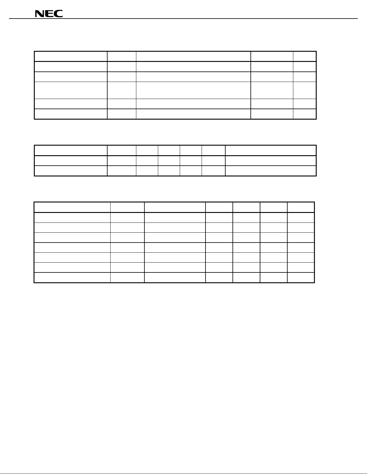
ABSOLUTE MAXIMUM RATINGS
PARAMETER SYMBOL CONDITION RATINGS UNIT
µµµµ
PB1508GV
Supply voltage V
Input voltage V
Total power dissipation P
CC
in
D
TA = +25 °C 6.0 V
TA = +25 °C 6.0 V
Mounted on double sided copper clad
50 × 50 × 1.6 mm epoxy glass PWB (T
Operating ambient temperature T
Storage temperature T
A
stg
RECOMMENDED OPERATING CONDITIONS
PARAMETER SYMBOL MIN. TYP. MAX. UNIT REMARKS
Supply voltage V
Operating ambient temperature T
ELECTRICAL CHARACTERISTICS (TA =
PARAMETER SYMBOL TEST CONDITION MIN. TYP. MAX. UNIT
Circuit current I
Upper limit operating frequency 1 f
Upper limit operating frequency 2 f
Lower limit operating frequency f
Input power 1 P
Input power 2 P
Output power P
CC
A
CC
in(U)1
in(U)2
in(L)
4.5 5.0 5.5 V
−
40 to +85
−−−−
in1
in2
out
250 mW
A
= +85 °C)
40 to +85
−
55 to +150
−
40 +25 +85
C, VCC = 4.5 to 5.5 V, ZS = ZL = 50
°°°°
C
°
)
ΩΩΩΩ
No signals 7.6 12 14.5 mA
Pin = −10 to +6 dBm 3.0
Pin = −15 to +6 dBm 2.7
Pin = −15 to +6 dBm
fin = 2.7 to 3.0 GHz
fin = 0.5 to 2.7 GHz
Pin = 0 dBm, fin = 2 GHz
10
−
15
−
12
−
0.5 GHz
−
7
+6 dBm
+6 dBm
GHz
GHz
dBm
C
°
C
°
4
Page 5

TYPICAL CHARACTERISTICS (unless otherwise specified TA = +25°C)
CIRCUIT CURRENT vs. SUPPLY VOLTAGE
15
No signals
TA = +85 ˚C
10
µµµµ
PB1508GV
TA = +25 ˚C
5
- Circuit Current - mA
CC
I
0
0123
V
CC
- Supply Voltage - V
INPUT POWER vs. INPUT FREQUENCY
+20
TA = +25 ˚C
+10
VCC = 4.5 to 5.5 V
0
–10
–20
- Input Power - dBm
–30
in
P
VCC = 4.5 to 5.5 V
–40
–50
TA = –40 ˚C
456
Guaranteed
Operating
Window
INPUT POWER vs. INPUT FREQUENCY
+20
VCC = 4.5 to 5.5 V
+10
TA = –40 ˚C
TA = +85 ˚C
0
–10
TA = +85 ˚C
–20
- Input Power - dBm
–30
in
P
–40
–50
TA = +25 ˚C
Guaranteed
Operating
Window
TA = +25 ˚C
TA = –40 ˚C
–60
100 1000 4000
in
- Input Frequency - MHz
f
–60
100 1000 4000
in
-Input Frequency - MHz
f
OUTPUT POWER vs. INPUT FREQUENCY OUTPUT POWER vs. INPUT FREQUENCY
0
VCC = 5.0 V
P
–2
Z
–4
–6
–8
in
= 0 dBm
L
= 50 Ω
TA = +85 ˚C
TA = +25 ˚C
TA = –40 ˚C
TA = –40 ˚C
0
TA = +25 ˚C
P
–2
Z
–4
–6
–8
in
= 0 dBm
L
= 50 Ω
VCC = 5.5 V
VCC = 5.0 V
VCC = 4.5 V
TA = +85 ˚C
–10
- Output Power - dBm
out
–12
P
TA = +25 ˚C
–14
–16
100 1000 4000
f
in
- Input Frequency - MHz fin -Input Frequency - MHz
–10
- Output Power - dBm
out
–12
P
–14
–16
100 1000 4000
5
Page 6

µµµµ
PB1508GV
OUTPUT POWER vs. INPUT FREQUENCY
0
TA = –40 ˚C
P
in
= 0 dBm
–2
Z
L
= 50 Ω
–4
–6
–8
–10
- Output Power - dBm
out
P
–12
–14
–16
100 1000 4000
in
- Input Frequency - MHz
f
S11 vs. INPUT FREQUENCY
VCC = 5.0 V
S
11
REF 1.0 Units
200.0 mUnits/
4
34.604 Ω –26.496 Ω
hp
C
MARKER 4
3.0 GHz
D
Z
START 0.500000000 GHz
STOP 3.000000000 GHz
VCC = 5.0 V
4
3
VCC = 5.5 V
VCC = 4.5 V
2
OUTPUT POWER vs. INPUT FREQUENCY
0
TA = +85 ˚C
P
in
= 0 dBm
–2
Z
L
= 50 Ω
–4
–6
VCC = 5.0 V
VCC = 5.5 V
–8
VCC = 4.5 V
–10
- Output Power - dBm
out
P
–12
–14
–16
100 1000 4000
f
in
- Input Frequency - MHz
FREQUENCY S
11
MHz MAG ANG
500.0000 .850 –30.2
600.0000 .796 –37.8
700.0000 .790 –39.2
800.0000 .754 –45.2
900.0000 .766 –53.7
1000.0000 .701 –57.6
1100.0000 .660 –62.3
: 500 MHz
1
: 1000 MHz
2
: 2000 MHz
3
: 3000 MHz
4
1
1200.0000 .606 –67.2
1300.0000 .571 –70.3
1400.0000 .521 –70.6
1500.0000 .495 –68.3
1600.0000 .441 –60.6
1700.0000 .479 –45.1
1800.0000 .602 –62.3
1900.0000 .595 –74.2
2000.0000 .608 –82.9
2100.0000 .603 –89.8
2200.0000 .599 –97.3
2300.0000 .588 –107.7
2400.0000 .532 –122.0
2500.0000 .396 –132.0
2600.0000 .325 –127.1
2700.0000 .270 –123.6
2800.0000 .232 –122.7
2900.0000 .258 –105.8
3000.0000 .351 –103.7
6
Page 7

S22 vs. OUTPUT FREQUENCY
VCC = 5.0 V, fin = 498 MHz
S22 Z
REF 1.0 Units
200.0 mUnits/
4
87.789 Ω –13.633 Ω
hp
C
MARKER 4
1.5 GHz
D
1
2
START 0.250000000 GHz
STOP 1.500000000 GHz
µµµµ
PB1508GV
FREQUENCY S
22
MHz MAG ANG
250.0000 .526 118.9
300.0000 .463 131.2
350.0000 .466 124.7
400.0000 .460 117.1
450.0000 .441 110.2
500.0000 .456 103.0
550.0000 .353 94.8
: 250 MHz
3
4
1
: 500 MHz
2
: 1000 MHz
3
: 1500 MHz
4
600.0000 .438 91.1
650.0000 .444 83.9
700.0000 .436 78.3
750.0000 .435 71.8
800.0000 .431 65.9
850.0000 .431 60.3
900.0000 .431 53.7
950.0000 .408 49.2
1000.0000 .445 44.9
1050.0000 .428 41.0
1100.0000 .429 33.7
1150.0000 .355 42.7
1200.0000 .418 20.0
1250.0000 .403 17.1
1300.0000 .392 9.6
1350.0000 .368 3.3
1400.0000 .343 –3.4
1450.0000 .319 –9.2
1500.0000 .289 –14.1
S22 vs. OUTPUT FREQUENCY
VCC = 5.0 V, fin = 3002 MHz
S22 Z
REF 1.0 Units
200.0 mUnits/
4
91.109 Ω 2.6523 Ω
hp
C
MARKER 4
1.5 GHz
D
2
1
START 0.250000000 GHz
STOP 1.500000000 GHz
FREQUENCY S
22
MHz MAG ANG
250.0000 .555 146.6
300.0000 .545 139.9
350.0000 .571 136.1
400.0000 .529 127.9
450.0000 .521 122.4
500.0000 .515 116.9
550.0000 .510 104.5
3
4
: 250 MHz
1
: 500 MHz
2
: 1000 MHz
3
: 1500 MHz
4
600.0000 .492 106.6
650.0000 .487 100.9
700.0000 .482 95.3
750.0000 .473 89.9
800.0000 .461 83.8
850.0000 .454 78.4
900.0000 .449 72.3
950.0000 .430 69.6
1000.0000 .443 64.3
1050.0000 .444 58.8
1100.0000 .440 52.3
1150.0000 .438 46.0
1200.0000 .501 37.5
1250.0000 .408 32.9
1300.0000 .388 25.1
1350.0000 .359 16.3
1400.0000 .335 9.7
1450.0000 .304 3.1
1500.0000 .285 4.6
7
Page 8

TEST CIRCUIT
Power Supply
µµµµ
PB1508GV
Signal Generator
50 Ω
HP8665A
1000 pF
1000 pF
C1
1000 pF
1000 pF
C2
C3
5 V±0.5 V
1
2
3
4
8
OPEN
1000 pF
7
C4
OPEN
6
5
Counter HP5350B
(Spectrum Analyzer)
50 Ω
8
Page 9

ILLUSTRATION OF THE TEST CIRCUIT ASSEMBLED ON EVALUATION BOARD
,,,,
,,
,
1P
VCC
µµµµ
PB1508GV
IN OUT
COMPONENT LIST
SYMBOL VALUE
C1 to C4 1000 pF
IN
C2 C4
C1
C3
PB1506/08/09GV
µ
EVALUATION BOARD CHARACTERS
(1) 35
(2) Back side: GND pattern
(3) Solder plated patterns
(4)
(5)
(6)
m thick double-sided copper clad 50 × 50 × 0.4 mm
µ
polyimide board
: Through holes
°
of pin 3 : partern should be removed.
of pin 5 : short chip must be attached to be grounded.
OUT
The application circuits and their parameters are for reference only and are not intended for use in actual design-ins.
9
Page 10

PACKAGE DIMENSIONS
8 pin PLASTIC SSOP (175 mil) (unit : mm)
85
14
+7°
3°
4.94±0.2
µµµµ
PB1508GV
–3°
1.8 MAX.
0.1±0.1
1.5±0.1
0.575 MAX.
3.0 MAX.
0.65
0.3
+0.10
–0.05
+0.10
0.10
–0.05
0.15
0.5±0.2
M
3.2±0.1
0.87±0.2
0.15
10
Page 11

µµµµ
PB1508GV
NOTE CORRECT USE
(1) Observe precautions for handling because of electro-static sensitive devices.
(2) Form a ground pattern as wide as possible to minimize ground impedance (to prevent undesired operation).
(3) Keep the wiring length of the ground pins as short as possible.
(4) Connect a bypass capacitor (e.g. 1 000 pF) to the V
CC
pin.
RECOMMENDED SOLDERING CONDITIONS
This product should be soldered in the following recommended conditions. Other soldering methods and
conditions than the recommended conditions are to be consulted with our sales representatives.
PB1508GV
µµµµ
Soldering method Soldering conditions Recommended condition symbol
Infrared ray reflow Package peak temperature: 235 °C,
Hour: within 30 s. (more than 210 °C),
Time: 3 times, Limited days: no.*
VPS Package peak temperature: 215 °C,
Hour: within 40 s. (more than 200 °C),
Time: 3 times, Limited days: no.*
Wave soldering Soldering tub temperature: less than 260 °C,
Hour: within 10 s.,
Time: 1 time, Limited days: no.
Pin part heating Pin area temperature: less than 300 °C,
Hour: within 3 s./pin,
Limited days: no.*
It is the storage days after opening a dry pack, the storage conditions are 25 °C, less than 65 % RH.
*
IR35-00-3
VP15-00-3
WS60-00-1
Caution The combined use of soldering method is to be avoided (However, except the pin area heating
method).
For details of recommended soldering conditions for surface mounting, refer to information document
SEMICONDUCTOR DEVICE MOUNTING TECHNOLOGY MANUAL (C10535E).
11
Page 12

µµµµ
PB1508GV
ATTENTION
OBSERVE PRECAUTIONS
FOR HANDLING
ELECTROSTATIC
SENSITIVE
DEVICES
No part of this document may be copied or reproduced in any form or by any means without the prior written
consent of NEC Corporation. NEC Corporation assumes no responsibility for any errors which may appear in this
document.
NEC Corporation does not assume any liability for infringement of patents, copyrights or other intellectual
property rights of third parties by or arising from use of a device described herein or any other liability arising
from use of such device. No license, either express, implied or otherwise, is granted under any patents,
copyrights or other intellectual property rights of NEC Corporation or others.
While NEC Corporation has been making continuous effort to enhance the reliability of its semiconductor devices,
the possibility of defects cannot be eliminated entirely. To minimize risks of damage or injury to persons or
property arising from a defect in an NEC semiconductor device, customers must incorporate sufficient safety
measures in its design, such as redundancy, fire-containment, and anti-failure features.
NEC devices are classified into the following three quality grades:
"Standard", "Special", and "Specific". The Specific quality grade applies only to devices developed based on
a customer designated "quality assurance program" for a specific application. The recommended applications
of a device depend on its quality grade, as indicated below. Customers must check the quality grade of each
device before using it in a particular application.
Standard: Computers, office equipment, communications equipment, test and measurement equipment,
audio and visual equipment, home electronic appliances, machine tools, personal electronic
equipment and industrial robots
Special: Transportation equipment (automobiles, trains, ships, etc.), traffic control systems, anti-disaster
systems, anti-crime systems, safety equipment and medical equipment (not specifically designed
for life support)
Specific: Aircrafts, aerospace equipment, submersible repeaters, nuclear reactor control systems, life
support systems or medical equipment for life support, etc.
The quality grade of NEC devices is "Standard" unless otherwise specified in NEC's Data Sheets or Data Books.
If customers intend to use NEC devices for applications other than those specified for Standard quality grade,
they should contact an NEC sales representative in advance.
Anti-radioactive design is not implemented in this product.
M4 96. 5
 Loading...