

Page 1
DATA SHEET
BIPOLAR DIGITAL INTEGRATED CIRCUITS
PB1506GV,
PPPP
PB1507GV
PPPP
3GHz INPUT DIVIDE BY 256, 128, 64 PRESCALER IC
FOR ANALOG DBS TUNERS
The PPB1506GV and PPB1507GV are 3.0 GHz input, high division silicon prescaler ICs for analog DBS tuner
applications. These ICs divide-by-256, 128 and 64 contribute to produce analog DBS tuners with kit-use of 17 K
series DTS controller or standard CMOS PLL synthesizer IC. The PPB1506GV/PPB1507GV are shrink package
versions of the PPB586G/588G or PPB1505GR so that these smaller packages contribute to reduce the mounting
space replacing from conventional ICs.
The PPB1506GV and PPB1507GV are manufactured using NEC’s high fT NESAT™IV silicon bipolar process.
This process uses silicon nitride passivation film and gold electrodes. These materials can protect chip surface from
external pollution and prevent corrosion/migration. Thus, these ICs have excellent performance, uniformity and
reliability.
FEATURES
High toggle frequency : fin = 0.5 GHz to 3.0 GHz
x
High-density surface mounting : 8-pin plastic SSOP (175 mil)
x
Low current consumption : 5 V, 19 mA
x
Selectable high division :y256, y128, y64
x
Pin connection variation :PPB1506GV and PPB1507GV
x
APPLICATION
These ICs can use as a prescaler between local oscillator and PLL frequency synthesizer included modulus
prescaler. For example, following application can be chosen;
Analog DBS tuner’s synthesizer
x
Analog CATV converter synthesizer
x
ORDERING INFORMATION
PART NUMBER PACKAGE MARKING SUPPLYING FORM
P
PB1506GV-E1 8-pin plastic 1506 Embossed tape 8 mm wide. P i n 1 i s in tape pull-out
P
PB1507GV-E1
Remarks
SSOP (175 mil)
To order evaluation samples, please contact your local NEC sales office.
(Part number for sample order:
Caution: Electro-static sensitive devices
P
1507
PB1506GV, PPB1507GV)
direction. 1 000 p/reel.
Document No. P10767EJ3V0DS00 (3rd edition)
Date Published January 1998 N CP(K)
Printed in Japan
1996©
Page 2
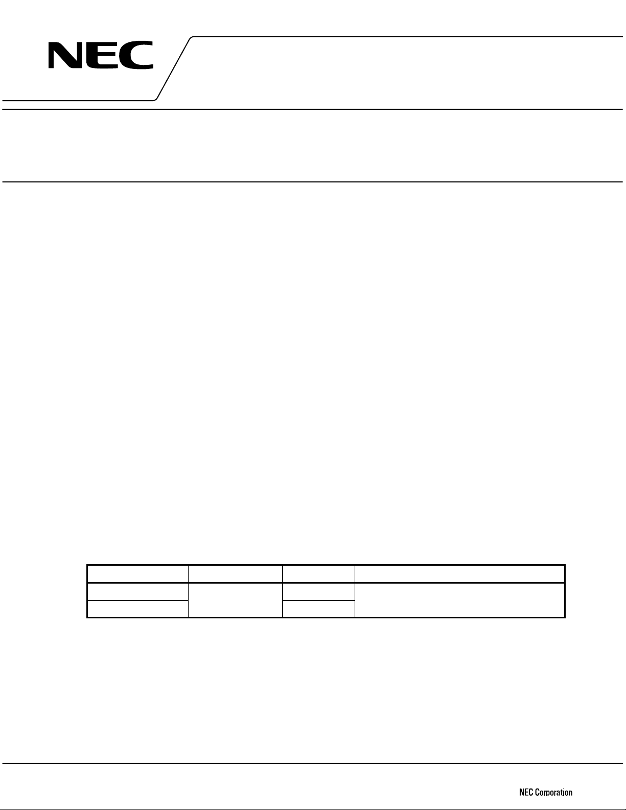
PIN CONNECTION (Top View)
5
6
7
8
4
3
2
1
PPPP
PB1506GV,
PPPP
PB1507GV
PRODUCT LINE-UP
Features
(division, Freq.)
512, y256, 2.5 GHz
y
128, y64, 2.5 GHz
y
256, y128, y64
y
3.0 GHz
Pin
NO.
1SW1 IN
2IN V
3IN SW1
4GND OUT
5NC GND
6SW2 SW2
7 OUT NC
8VCCIN
Part No.
PB586G 28 0.5 to 2.5 4.5 to 5.5 8 pin SOP 225 mil NEC original
P
PB588G 26 0.5 to 2.5 4.5 to 5.5
P
PB1505GR 14 0.5 to 3.0 4.5 to 5.5 Standard
P
PB1506GV 19 0.5 to 3.0 4.5 to 5.5 8 pin SSOP 175 mil NEC original
P
PB1507GV 19 0.5 to 3.0 4.5 to 5.5 Standard
P
CC
I
(mA)
in
f
(GHz)
V
(V)
CC
PB1506GV
P
Package Pin connection
PB1507GV
P
CC
Remarks
This table shows the TYP values of main parameters. Please refer to ELECTRICAL
x
CHARACTERISTICS.
PB586G and PPB588G are discontinued.
x
P
INTERNAL BLOCK DIAGRAM
D
IN
IN
CLK
CLKQQ
D
CLK
Q
Q
D
CLK
D
CLK
Q
Q
Q
Q
D
Q
CLK
Q
D
Q
CLK
Q
SW1 SW2
D
CLK
D
CLK
Q
Q
Q
OUT
Q
AMP
2
Page 3
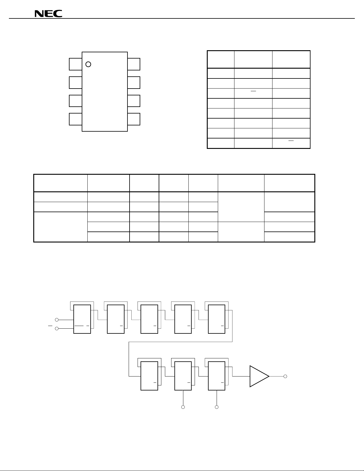
SYSTEM APPLICATION EXAMPLE
PPPP
PB1506GV,
RF unit block of Analog DBS tuners
PPPP
PB1507GV
1stIF input
from DBS converter
To 2150 MHz
To 800 MHz
MIX
BPF SAW AGC amp. FM demo.
High division prescaler
µ
OSC
To 2650 MHz
PB1506GV or
µ
PB1507GV
LPF
loop filter
RF unit block of Analog CATV converter
upconverter
BPF BPF
downconverter
To 1300 MHz
Baseband output
CMOS
PLL
synthesizer
OSC
To 2000 MHz
High division prescaler
µ
PB1506GV or
µ
PB1507GV
LPF
loop filter
CMOS
PLL
synthesizer
3
Page 4
PIN EXPLANATION
PPPP
PB1506GV,
PPPP
PB1507GV
Pin name
IN
IN
GND 0
SW1 H/L
SW2
CC
V
OUT
NC
4.5 to 5.5
Applied
voltage
V
•
•
•
••
Pin
voltage
V
2.9 Signal input pin. This pin should be coupled to signal
2.9 Signal input bypass pin. This pin must be equipped
•
•
•
2.6 to 4.7 Divided frequency output pin. This pin is designed as
Functions and explanation
source with capacitor (e.g. 1 000 pF) for DC cut.
with bypass capacitor (e.g. 1 000 pF) to minimize
ground impedance.
Ground pin. Ground pattern on the board should be
formed as wide as possible to minimize ground
impedance.
Divide ratio input pin. The ratio can be determined by
following applied level to these pins.
SW2
HL
H
SW1
These pins should be equipped with bypass capacitor
(e.g. 1 000 pF) to minimize ground impedance.
Power supply pin. This pin must be equipped with
bypass capacitor (e.g. 10 000 pF) to minimize ground
impedance.
emitter follower output. This pin can be connected to
CMOS input due to 1.2 V
Non connection pin. This pin must be openned. 5 7
y64y
Ly128y256
P-P
MIN output.
128
PB1506GV
P
Pin no.
PB1507GV
P
21
38
45
13
66
82
74
4
Page 5
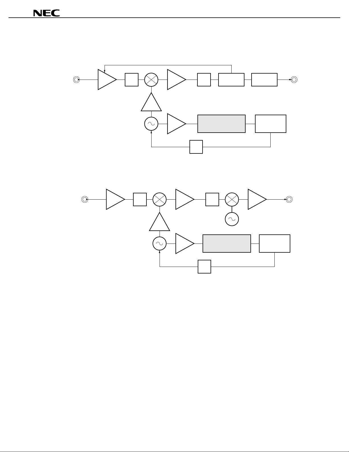
ABSOLUTE MAXIMUM RATINGS
PARAMETER SYMBOL CONDITION RATINGS UNIT
PPPP
PB1506GV,
PPPP
PB1507GV
Supply voltage V
Input voltage V
Total power dissipation P
Operating ambient temperature T
Storage temperature T
CC
in
D
A
stg
RECOMMENDED OPERATING CONDITIONS
PARAMETER SYMBOL MIN. TYP. MAX. UNIT NOTICE
Supply voltage V
Operating ambient temperature T
ELECTRICAL CHARACTERISTICS (TA =
PARAMETER SYMBOL TEST CONDIT ION MIN. TYP. MAX. UNIT
Circuit current I
Upper limit operating frequency f
Lower limit operating frequency 1 f
Lower limit operating frequency 2 f
Input power 1 P
Input power 2 P
Output Voltage V
Divide ratio control input high V
Divide ratio control input low V
Divide ratio control input high V
Divide ratio control input low V
CC
CC
in(u)
in(L)1
in(L)2
in1
in2
out
IH1
IL1
IH2
IL2
A
40 to +85
ðððð
TA = +25 qC
TA = +25 qC
Mounted on double sided copper clad
50 u 50 u 1.6 mm epoxy glass PWB (T
A
=
0.5 to +6.0 V
ð
0.5 to VCC + 0.5 V
ð
250 mW
+85 qC)
40 to +85
ð
55 to +150
ð
q
q
4.5 5.0 5.5 V
40 +25 +85
ð
C, VCC = 4.5 to 5.5 V, ZS = 50
qqqq
C
q
)
::::
No signals 12.5 19 26.5 mA
Pin = ð15 to +6 dBm 3.0
Pin = ð10 to +6 dBm
Pin = ð15 to +6 dBm
fin = 1.0 to 3.0 GHz
fin = 0.5 to 1.0 GHz
••
••
ð
ð
15
10
••
•
•
CL = 8 pF 1.2 1.6
Connection in the test
CC
V
V
0.5 GHz
1.0 GHz
+6 dBm
+6 dBm
•
CC
CC
V
GHz
V
circuit
Connection in the test
circuit
Connection in the test
OPEN or
GND
CC
V
OPEN or
GND
CC
V
OPEN or
GND
CC
V
circuit
Connection in the test
circuit
OPEN or
GND
OPEN or
GND
OPEN or
GND
C
C
P-P
5
Page 6
PPPP
PB1506GV,
PPPP
PB1507GV
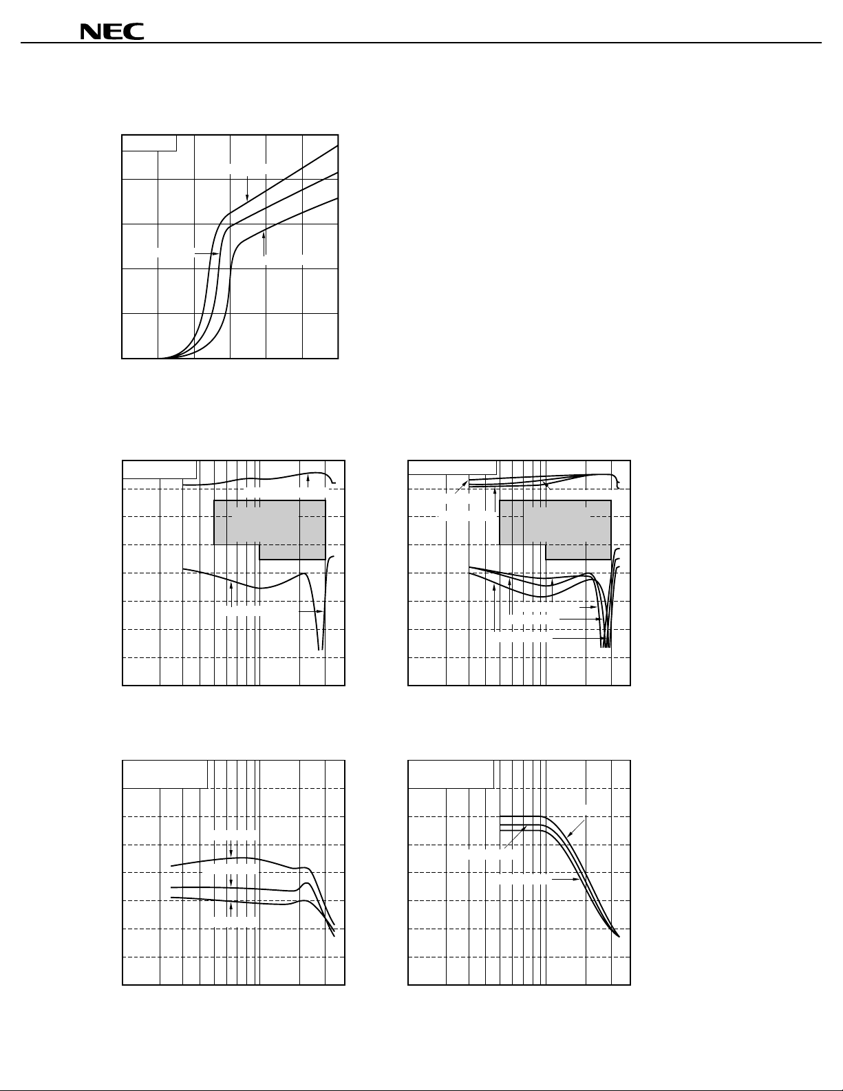
TYPICAL CHARACTERISTICS (Unless otherwise specified TA = +25
CIRCUIT CURRENT vs. SUPPLY VOLTAGE
25
No signals
20
TA = +85°C
15
TA = +25°C
0
- Circuit Current - mA
CC
I
TA = –40°C
5
0
0123
V
CC
- Supply Voltage - V
456
Divide by 64 mode
INPUT POWER vs. INPUT FREQUENCY
+20
TA = +25°C
+10
0
–10
VCC = 4.5 to 5.5 V
Guaranteed
Operating
Window
INPUT POWER vs. INPUT FREQUENCY
+20
VCC = 4.5 to 5.5 V
+10
TA = –40°C
0
TA = +85°C
–10
C)
qqqq
TA = +25°C
Guaranteed
Operating
Window
–20
- Input Power - dBm
–30
in
P
VCC = 4.5 to 5.5 V
–40
–50
–60
100 1000 4000
in
- Input Frequency - MHz
f
OUTPUT VOLTAGE vs.INPUT FREQUENCY
2.0
TA = +25°C
P
in
= –10 dBm
1.9
P-P
1.8
1.7
1.6
- Output Voltage - V
1.5
out
V
1.4
VCC = 5.5 V
VCC = 5.0 V
VCC = 4.5 V
1.3
–20
- Input Power - dBm
–30
in
P
–40
TA = +85°C
TA = +25 °C
TA = –40°C
–50
–60
100 1000 4000
in
- Input Frequency - MHz
f
OUTPUT VOLTAGE vs.INPUT FREQUENCY
2.0
TA = –40°C
P
in
= –10 dBm
1.8
P-P
1.6
1.4
VCC = 5.0 V
1.2
- Output Voltage - V
1.0
out
V
VCC = 4.5 V
VCC = 5.5 V
0.8
0.6
1.2
100 1000 4000
in
- Input Frequency - MHz
f
6
0.4
100 1000 4000
in
- Input Frequency - MHz
f
Page 7

OUTPUT VOLTAGE vs. INPUT RFEQUENCY
2.0
TA = +85°C
P
in
= –10 dBm
1.8
P-P
VCC = 5.5 V
1.6
1.4
1.2
- Output Voltage - V
1.0
out
V
VCC = 4.5 V
0.8
0.6
0.4
100 1000 4000
in
- Input Frequency - MHz
f
Divide by 128 mode
VCC = 5.0 V
PPPP
PB1506GV,
PPPP
PB1507GV
INPUT POWER vs. INPUT FREQUENCY
+20
TA = +25°C
+10
VCC = 4.5 to 5.5 V
0
–10
Guaranteed
Operating
Window
–20
- Input Power - dBm
–30
in
P
VCC = 4.5 to 5.5 V
–40
–50
–60
100 1000 4000
in
- Input Frequency - MHz
f
OUTPUT VOLTAGE vs. INPUT FREQUENCY
2.0
TA = +25°C
P
in
= –10 dBm
1.9
P-P
1.8
1.7
1.6
- Output Voltage - V
1.5
out
V
1.4
VCC = 5.5 V
VCC = 5.0 V
VCC = 4.5 V
INPUT POWER vs. INPUT FREQUENCY
+20
VCC = 4.5 to 5.5 V
+10
0
–10
TA = –40°C
TA = +85°C
TA = +25°C
Guaranteed
Operating
Window
–20
- Input Power - dBm
–30
in
P
–40
TA = +85°C
TA = +25°C
TA = –40°C
–50
–60
100 1000 4000
in
- Input Frequency - MHz
f
OUTPUT VOLTAGE vs. INPUT FREQUENCY
2.0
TA = –40°C
P
in
= –10 dBm
1.9
P-P
1.8
1.7
1.6
- Output Voltage - V
1.5
out
V
1.4
VCC = 5.5 V
VCC = 5.0 V
VCC = 4.5 V
1.3
1.2
100 1000 4000
in
- Input Frequency - MHz
f
1.3
1.2
100 1000 4000
in
- Input Frequency - MHz
f
7
Page 8

OUTPUT VOLTAGE vs. INPUT FREQUENCY
2.0
TA = +85°C
P
in
= –10 dBm
1.9
P-P
1.8
PPPP
PB1506GV,
PPPP
PB1507GV
1.7
VCC = 5.5 V
1.6
VCC = 5.0 V
- Output-Voltage - V
1.5
out
V
1.4
VCC = 4.5 V
1.3
1.2
100 1000 4000
in
- Input Frequency - MHz
f
Divide by 256 mode
INPUT POWER vs. INPUT FREQUENCY
+20
TA = +25°C
+10
VCC = 4.5 to 5.5 V
0
–10
–20
- Input Power - dBm
–30
in
P
–40
–50
Guaranteed
Operating
Window
VCC = 4.5 to 5.5 V
INPUT POWER vs. INPUT FREQUENCY
+20
VCC = 4.5 to 5.5 V
+10
TA = –40°C
TA = +85°C
0
TA = +25°C
–10
–20
- Input Power - dBm
–30
in
P
–40
–50
Guaranteed
Operating
Window
TA = +85°C
TA = +25°C
TA = –40 °C
–60
100 1000 4000
in
- Input Frequency - MHz
f
OUTPUT VOLTAGE vs. INPUT FREQUENCY
2.0
TA = +25°C
P
in
= –10 dBm
1.9
P-P
1.8
1.7
VCC = 5.5 V
VCC = 5.0 V
1.6
- Output Voltage - V
1.5
out
V
1.4
VCC = 4.5 V
1.3
1.2
100 1000 4000
in
- Input Frequency - MHz
f
8
–60
100 1000 4000
in
- Input Frequency - MHz
f
OUTPUT VOLTAGE vs. INPUT FREQUENCY
2.0
TA = –40°C
P
in
= –10 dBm
1.9
P-P
1.8
1.7
VCC = 5.5 V
VCC = 5.0 V
1.6
- Output Voltage - V
1.5
out
V
1.4
VCC = 4.5 V
1.3
1.2
100 1000 4000
f
in
- Input Frequency - MHz
Page 9

OUTPUT VOLTAGE vs. INPUT FREQUENCY
2.0
TA = +85°C
P
in
= –10 dBm
1.9
P-P
1.8
1.7
VCC = 5.5 V
VCC = 5.0 V
1.6
- Output Voltage - V
1.5
out
V
1.4
VCC = 4.5 V
1.3
1.2
100 1000 4000
in
- Input Frequency - MHz
f
PB1506GV
PPPP
11
S
vs. INPUT FREQUENCY
VCC = 5.0 V
S
11
REF 1.0 Units
200.0 mUnits/
3
33.881 Ω –52.875 Ω
hp
∗
C
MARKER 3
2.0 GHz
D
Z
START
STOP
4
3
2
0.500000000 GHz
3.000000000 GHz
PPPP
PB1506GV,
FREQUENCY S
PPPP
PB1507GV
11
MHz MAG ANG
500.0000 .868 –26.6
600.0000 .828 –32.6
700.0000 .794 –37.4
800.0000 .761 –41.9
900.0000 .721 –46.5
1000.0000 .706 –49.3
1100.0000 .662 –54.0
: 500 MHz
1
: 1000 MHz
2
: 2000 MHz
3
: 3000 MHz
4
1
1200.0000 .629 –57.2
1300.0000 .595 –60.2
1400.0000 .554 –62.9
1500.0000 .516 –64.8
1600.0000 .440 –61.9
1700.0000 .428 –51.0
1800.0000 .543 –61.5
1900.0000 .555 –68.4
2000.0000 .560 –74.7
2100.0000 .558 –79.5
2200.0000 .564 –84.9
2300.0000 .570 –90.9
2400.0000 .574 –98.3
2500.0000 .574 –107.9
2600.0000 .564 –118.3
2700.0000 .530 –131.4
2800.0000 .476 –144.6
2900.0000 .411 –159.1
3000.0000 .331 –175.8
9
Page 10

PB1506GV
PPPP
22
S
vs. OUTPUT FREQUENCY
Divide by 64 mode, V
S22 Z
REF 1.0 Units
200.0 mUnits/
1
171.22 Ω –04.438 Ω
CC
hp
∗
C
MARKER 1
45.0 MHz
D
= 5.0 V
PPPP
PB1506GV,
FREQUENCY S
MHz MAG ANG
45.000 .542 –1.4
50.000 .602 –.3
55.000 .616 0.0
60.000 .605 1.1
65.000 .609 .7
70.000 .616 .3
75.000 .620 .1
: 45 MHz
1
1
2
: 100 MHz
2
80.000 .622 0.0
85.000 .619 .6
90.000 .610 .9
95.000 .626 –.7
100.000 .623 –1.7
PPPP
PB1507GV
22
START
STOP
PB1506GV
PPPP
22
S
vs. OUTPUT FREQUENCY
0.045000000 GHz
0.100000000 GHz
Divide by 128 mode, VCC = 5.0 V
S22
REF 1.0 Units
200.0 mUnits/
1
192.34 Ω 03.109 Ω
hp
C
MARKER 1
45.0 MHz
D
Z
FREQUENCY S
MHz MAG ANG
45.000 .590 .4
50.000 .604 –1.0
55.000 .610 –1.1
60.000 .607 –.8
65.000 .548 –5.9
70.000 .630 –0.0
: 45 MHz
1
1
2
: 100 MHz
2
75.000 .615 –1.0
80.000 .618 –1.4
85.000 .617 –1.2
90.000 .616 –2.2
95.000 .623 –2.4
100.000 .624 –2.3
22
10
START
STOP
0.045000000 GHz
0.100000000 GHz
Page 11

PB1506GV
PPPP
22
S
vs. OUTPUT FREQUENCY
Divide by 256 mode, V
S22
CC
Z
REF 1.0 Units
200.0 mUnits/
1
199.25 Ω –05.992 Ω
hp
C
MARKER 1
45.0 MHz
D
= 5.0 V
PPPP
PB1506GV,
FREQUENCY S
PPPP
PB1507GV
22
MHz MAG ANG
45.000 .601 –.9
50.000 .609 –1.6
55.000 .611 –1.5
60.000 .620 –1.4
65.000 .607 –2.1
70.000 .615 –1.9
75.000 .613 –3.2
: 45 MHz
1
1
2
: 100 MHz
2
80.000 .611 –2.8
85.000 .607 –2.5
90.000 .605 –2.4
95.000 .610 –3.0
100.000 .608 –2.8
START
STOP
PB1507GV
PPPP
11
S
vs. INPUT FREQUENCY
VCC = 5.0 V
S
11
REF 1.0 Units
200.0 mUnits/
4
38.111 Ω 0.9707 Ω
hp
C
MARKER 4
3.0 GHz
D
Z
START
STOP
0.045000000 GHz
0.100000000 GHz
4
3
2
0.500000000 GHz
3.000000000 GHz
FREQUENCY S
11
MHz MAG ANG
500.0000 .857 –27.5
600.0000 .849 –32.0
700.0000 .800 –38.9
800.0000 .764 –43.8
900.0000 .725 –49.0
1000.0000 .665 –50.9
1100.0000 .619 –55.3
: 500 MHz
1
: 1000 MHz
2
: 2000 MHz
3
: 3000 MHz
4
1
1200.0000 .573 –59.3
1300.0000 .531 –61.3
1400.0000 .484 –62.8
1500.0000 .439 –63.0
1600.0000 .377 –59.1
1700.0000 .340 –54.1
1800.0000 .377 –54.7
1900.0000 .441 –59.5
2000.0000 .464 –67.2
2100.0000 .443 –67.4
2200.0000 .466 –74.5
2300.0000 .465 –81.3
2400.0000 .454 –89.4
2500.0000 .433 –99.2
2600.0000 .383 –109.6
2700.0000 .350 –114.0
2800.0000 .332 –124.2
2900.0000 .271 –141.2
3000.0000 .185 –163.6
11
Page 12

PB1507GV
PPPP
22
S
vs. OUTPUT FREQUENCY
Divide by 64 mode, V
S22
REF 1.0 Units
200.0 mUnits/
1
185.13 Ω 17.789 Ω
CC
Z
hp
C
MARKER 1
45.0 MHz
D
= 5.0 V
PPPP
PB1506GV,
FREQUENCY S
MHz MAG ANG
45.000 .580 3.4
50.000 .572 2.5
55.000 .574 3.0
60.000 .574 2.7
65.000 .584 3.0
70.000 .587 2.6
75.000 .592 2.4
: 45 MHz
1
1
2
: 100 MHz
2
80.000 .587 2.6
85.000 .589 2.9
90.000 .591 2.9
95.000 .573 1.7
100.000 .604 2.9
PPPP
PB1507GV
22
START
STOP
PB1507GV
PPPP
22
S
vs. OUTPUT FREQUENCY
0.045000000 GHz
0.100000000 GHz
Divide by 128 mode, VCC = 5.0 V
S
22
REF 1.0 Units
200.0 mUnits/
1
185.02 Ω 18.953 Ω
hp
C
MARKER 1
45.0 MHz
D
Z
FREQUENCY S
MHz MAG ANG
45.000 .578 3.2
50.000 .571 2.8
55.000 .572 3.3
60.000 .576 3.0
65.000 .584 3.1
70.000 .587 2.8
75.000 .589 2.4
: 45 MHz
1
1
2
: 100 MHz
2
80.000 .589 2.8
85.000 .588 3.0
90.000 .593 2.8
95.000 .598 3.0
100.000 .602 2.9
22
12
START
STOP
0.045000000 GHz
0.100000000 GHz
Page 13

PB1507GV
PPPP
22
S
vs. OUTPUT FREQUENCY
Divide by 256 mode, V
S22
REF 1.0 Units
200.0 mUnits/
1
186.76 Ω 17.82 Ω
hp
C
MARKER 1
45.0 MHz
D
CC
Z
= 5.0 V
PPPP
PB1506GV,
FREQUENCY S
MHz MAG ANG
45.000 .580 3.0
50.000 .572 2.8
55.000 .571 2.9
60.000 .576 2.9
65.000 .585 3.2
70.000 .590 2.8
75.000 .589 2.5
: 45 MHz
1
2
1
: 100 MHz
2
80.000 .590 2.6
85.000 .588 2.9
90.000 .597 2.9
95.000 .600 3.1
100.000 .601 3.1
PPPP
PB1507GV
22
START
STOP
0.045000000 GHz
0.100000000 GHz
13
Page 14

TEST CIRCUIT
PB1506GV
PPPP
PPPP
PB1506GV,
PPPP
PB1507GV
SW1
1
C1
C2
2
C3
3
4
IN
IN
GND
50 Ω
S.G
VCC = +5.0 V
±10 %
C6
SG (HP-8665A)
x
Counter (HP5350B) : To measure input sensitivity
x
or
Oscilloscope : To measure output voltage swing
V
OUT
SW2
NC
CC
8
C7
C5
7
6
C4
OPEN
5
Stray cap.
Monitor
1 MΩ
0.6 pF
Oscilloscope
or Counter
50 Ω
Divide ratio setting
SW2
HL
COMPONENT LIST
PB1506GV
P
C1 to C5 1 000 pF 1 000 pF
C6 10 000 pF 10 000 pF
Stray cap. Aprox 4 pF Aprox 5 pF
3.5 pF
C7
*
PB1507GV
P
2.5 pF*
* Capacitance CL = 8 pF for DUT includes
C7 value + stray capacitance on the
board and measurement equipment.
SW1 H 1/64 1/128
L 1/128 1/256
H: Connect to V
CC
L: Connect to GND or OPEN
14
Page 15

TEST CIRCUIT
PB1507GV
PPPP
PPPP
PB1506GV,
PPPP
PB1507GV
V
CC
= +5.0 V ±10%
S.G
50 Ω
C6
C7 Stray cap.
C2
1
IN
2
CC
V
SW1
3
C1 C4
OUT
4
C5
Monitor
1 MΩ
0.6 pF
Oscilloscope
or Counter
IN
NC
SW2
GND
8
7
OPEN
6
5
C3
SG (HP-8665A)
x
Counter (HP5350B) : To measure input sensitivity
x
or
Oscilloscope : To measure output voltage swing
50 Ω
Divide ratio setting
SW2
HL
SW1 H 1/64 1/128
L 1/128 1/256
H: Connect to V
CC
L: Connect to GND or OPEN
15
Page 16

PPPP
PB1506GV,
ILLUSTRATION OF THE TEST CIRCUIT ASSEMBLED ON EVALUATION BOARD
PB1506GV
PPPP
1P
PPPP
PB1507GV
PB1507GV
PPPP
SW1 V
IN OUT
IN
IN
IN
C2
C1
C3
PB1506/08/09GV
µ
1P
C6
C7
C5C2
C4
CC
OUT
SW2
OPEN
16
V
SW1
OUT
CC
C6C1
C5
C7
PB1507GVOUT
µ
EVALUATION BOARD CHARACTERS
(1) 35
m thick double-sided copper clad 50 u 50 u 0.4 mm
P
polyimide board
(2) Back side: GND pattern
(3) Solder plated patterns
(4)
: Through holes
q
C3
SW2
C4
Page 17

PACKAGE DIMENSIONS
8 PIN PLASTIC SSOP (UNIT: mm) (175 mil)
85
14
PPPP
PB1506GV,
detail of lead end
+7˚
–3˚
3˚
4.94 ±0.2
PPPP
PB1507GV
1.8 MAX.
0.1±0.1
1.5 ±0.1
0.575 MAX.
3.0 MAX.
0.65
0.3
+0.10
–0.05
+0.10
–0.05
0.15
0.10
0.5 ±0.2
M
3.2 ±0.1
0.87 ±0.2
0.15
17
Page 18

PPPP
PB1506GV,
NOTE CORRECT USE
(1) Observe precautions for handling because of electro-static sensitive devices.
(2) Form a ground pattern as wide as possible to minimize ground impedance (to prevent undesired operation).
(3) Keep the wiring length of the ground pins as short as possible.
CC
(4) Connect a bypass capacitor (e.g. 10 000 pF) to the V
RECOMMENDED SOLDERING CONDITIONS
This product should be soldered in the following recommended conditions. Other soldering methods and
conditions than the recommended conditions are to be consulted with our sales representatives.
pin.
PPPP
PB1507GV
PB1506GV,
PPPP
Soldering method Soldering conditions Recommended condition symbol
Infrared ray reflow Package peak temperature: 235 qC,
VPS
Wave soldering Soldering tub temperature: less than 260 qC,
Pin part heating Pi n area tem perature: less than 300 qC,
It is the storage days after opening a dry pack, the storage conditions are 25 qC, less than 65 % RH.
*
Caution The combined use of soldering method is to be avoided (However, except the pin area heating
PB1507GV
PPPP
method).
Hour: within 30 s. (more than 210 qC),
Time: 3 times, Limited days: no.*
Package peak temperature: 215 qC,
Hour: within 40 s. (more than 200 qC),
Time: 3 times, Limited days: no.*
Hour: within 10 s.,
Time: 1 time, Limited days: no.
Hour: within 3 s./pin,
Limited days: no.*
IR35-00-3
VP15-00-3
WS60-00-1
For details of recommended soldering conditions for surface mounting, refer to information document
SEMICONDUCTOR DEVICE MOUNTING TECHNOLOGY MANUAL (C10535E).
18
Page 19

[MEMO]
PPPP
PB1506GV,
PPPP
PB1507GV
19
Page 20

PPPP
PB1506GV,
PPPP
PB1507GV
ATTENTION
OBSERVE PRECAUTIONS
FOR HANDLING
ELECTROSTATIC
SENSITIVE
DEVICES
No part of this document may be copied or reproduced in any form or by any means without the prior written
consent of NEC Corporation. NEC Corporation assumes no responsibility for any errors which may appear in this
document.
NEC Corporation does not assume any liability for infringement of patents, copyrights or other intellectual
property rights of third parties by or arising from use of a device described herein or any other liability arising
from use of such device. No license, either express, implied or otherwise, is granted under any patents,
copyrights or other intellectual property rights of NEC Corporation or others.
While NEC Corporation has been making continuous effort to enhance the reliability of its semiconductor devices,
the possibility of defects cannot be eliminated entirely. To minimize risks of damage or injury to persons or
property arising from a defect in an NEC semiconductor device, customers must incorporate sufficient safety
measures in its design, such as redundancy, fire-containment, and anti-failure features.
NEC devices are classified into the following three quality grades:
"Standard", "Special", and "Specific". The Specific quality grade applies only to devices developed based on
a customer designated "quality assurance program" for a specific application. The recommended applications
of a device depend on its quality grade, as indicated below. Customers must check the quality grade of each
device before using it in a particular application.
Standard: Computers, office equipment, communications equipment, test and measurement equipment,
audio and visual equipment, home electronic appliances, machine tools, personal electronic
equipment and industrial robots
Special: Transportation equipment (automobiles, trains, ships, etc.), traffic control systems, anti-disaster
systems, anti-crime systems, safety equipment and medical equipment (not specifically designed
for life support)
Specific: Aircrafts, aerospace equipment, submersible repeaters, nuclear reactor control systems, life
support systems or medical equipment for life support, etc.
The quality grade of NEC devices is "Standard" unless otherwise specified in NEC's Data Sheets or Data Books.
If customers intend to use NEC devices for applications other than those specified for Standard quality grade,
they should contact an NEC sales representative in advance.
Anti-radioactive design is not implemented in this product.
M4 96. 5
 Loading...