

Page 1
DATA SHEET
BIPOLAR DIGITAL INTEGRATED CIRCUIT
µ
PB1505GR
3.0 GHz PRESCALER DIVIDED BY 256, 128, 64
FOR BS/CS TUNER
DESCRIPTION
µ
PB1505GR is a silicon prescaler IC operating up to 3.0 GHz and divided by 256, 128, 64. Due to 3.0 GHz operation and
high division, this IC can contribute to produce BS/CS tuners with kit-use of 17K series DTS controller or standard CMOS
PLL IC. The package is 8 pin plastic SOP suitable for surface mounting.
This IC is manufactured using NEC’s 20 GHz f
passivation film and gold electrodes. These materials can protect the chips from external pollution and prevent corrosion/
migration. Thus, this IC has with excellent performance, uniformity and reliability.
T NESAT
III silicon bipolar process. This process uses silicon nitride
FEATURES
• High toggle-frequency : 0.5 GHz to 3.0 GHz
• Low power-consumption : 14 mA TYP. at 5 V
• High divide-ratio : ÷256, ÷128, ÷64
• High input-sensitivity : –14 to +10 dBm @ 1.0 GHz to 2.7 GHz
• Wide output-swing : 1.6 Vp-p (CL = 8 pF load)
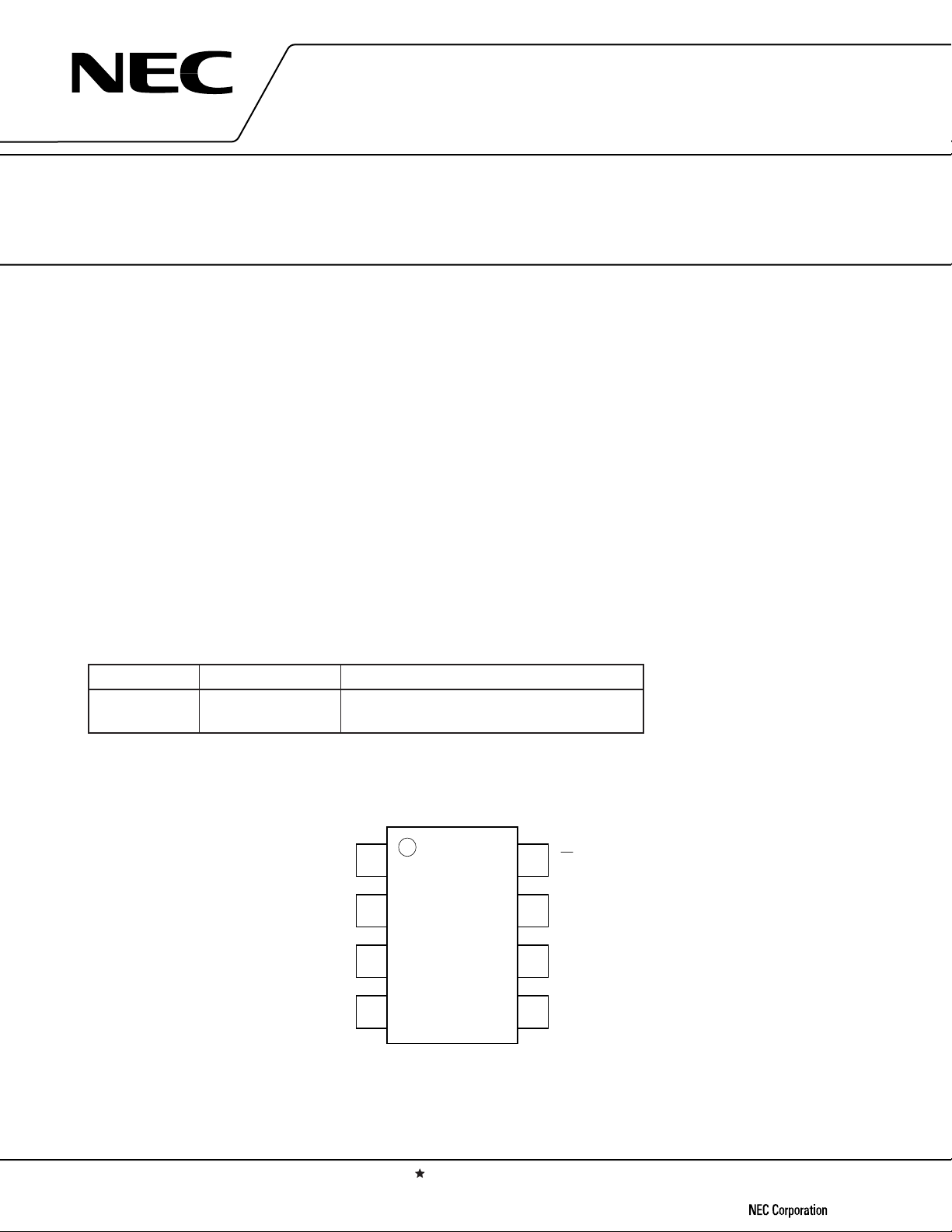
ORDERING INFORMATION
PART NUMBER PACKAGE SUPPLYING FORM
µ
PB1505GR-E1
Remarks To order evaluation samples, please contact your local NEC sales office. (Order number : µPB1505GR)
8 pin plastic SOP Embossed tape 12 mm wide. QTY 2.5 k/reel
(225 mil) Pin 1 is in tape pull-out direction.
PIN ASSIGNMENT (Top View)
IN
1
V
2
CC
8
IN
7
GND
The information in this document is subject to change without notice. Before using this document, please
confirm that this is the latest version.
Not all devices/types available in every country. Please check with local NEC representative for availability
and additional information.
Document No. P10872EJ3V0DS00 (3rd edition)
Date Published October 1999 N CP(K)
Printed in Japan
SW1
OUT
3
4
Caution electro-static sensitive devices
The mark shows major revised points.
6
5
SW2
GND
©
1996,1999
Page 2
SELECTOR GUIDE
µ
PB1505GR
FEATURES
2.5 GHz / ÷512, ÷256
2.5 GHz / ÷128, ÷64
3.0 GHz / ÷256, ÷128, ÷64
PRODUCT ICC fin VCC
NUMBER (mA) (GHz) (V)
µ
PB586G 28 0.5 to 2.5 5 8 pin SOP
µ
PB588G 26 0.5 to 2.5 5 8 pin SOP
µ
PB1505GR 14 0.5 to 3.0 5 8 pin SOP Typical of prescaler
Notice Typical performance. Please refer to Electrical Characteristics in detail.
To know the associated products, please refer to their latest data sheets.
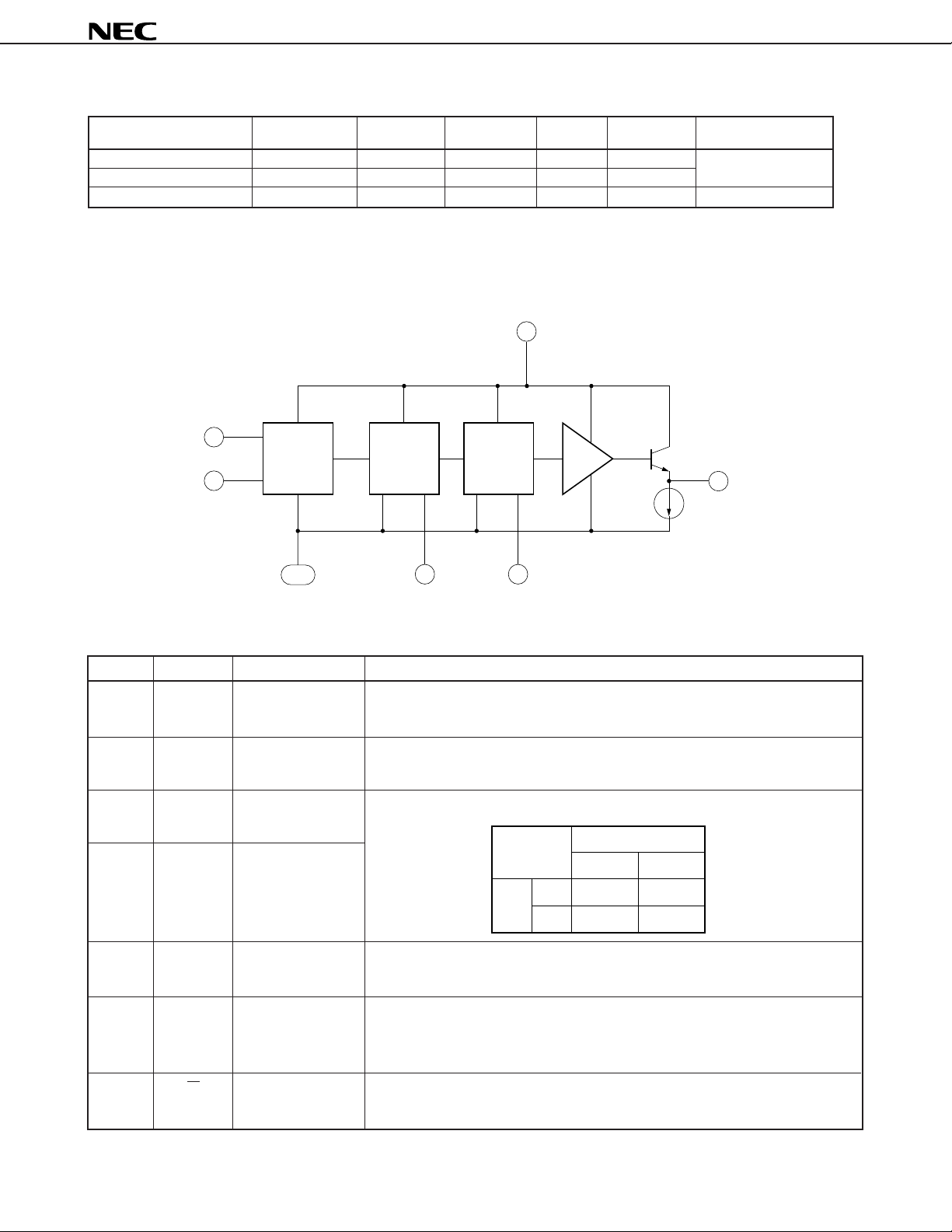
INTERNAL BLOCK DIAGRAM
CC
V
2
INPUT
BYPASS
1
1 / 64 1 / 2 1 / 2 Buff.
8
5, 7
GND SW1 SW2
36
PACKAGE PIN ASSIGNMENT
NEC original
OUTPUT
4
PIN DESCRIPTIONS
PIN NO. SYMBOL ASSIGNMENT FUNCTIONS AND EXPLANATION
1 IN Frequency input
pin
2VCC Power supply pin
3 SW1 Divided ratio
control input pin 1
6 SW2 Divided ratio
control input pin 2
4 OUT Divided frequency
output pin
5 GND Ground pin
7
Input frequency from an external VCO output.
Must be coupled with capacitor (e.g. 1 000 pF) for DC cut.
Supply voltage 5.0±0.5 V for operation. Must be connected bypass capacitor
(e.g. 1 000 pF) to minimize ground impedance.
Divided ratio control can be governed by following input data to these pins.
SW2
HL
SW1
H
L
This frequency output can be interfaced to CMOS PLL.
Must be coupled with capacitor (e.g. 1 000 pF) for DC cut.
This pin must be connected to the system ground with minimum inductance.
Ground pattern on the board should be formed as wide as possible.
(Track length should be kept as short as possible.)
1/64 1/128
1/128
1/256
8 IN Frequency-input
bypass pin
2
This pin must be connected bypass capacitor (e.g. 1 000 pF) to minimize ground
impedance.
Data Sheet P10872EJ3V0DS00
Page 3
ABSOLUTE MAXIMUM RATINGS
PARAMETER SYMBOL RATING UNIT CONDITIONS
Supply voltage VCC –0.5 to +6 V TA = +25 °C
Input voltage VIN –0.5 to VCC +0.5 V TA = +25 °C
µ
PB1505GR
Power dissipation PD 250 mW
Operating temperature Topt –40 to +85 °C
Storage temperature Tstg –55 to +150 °C
Mounted on 50 × 50 × 1.6 mm double copper clad
epoxy glass PWB (TA = +85 °C)
RECOMMENDED OPERATING RANGE
PARAMETER SYMBOL MIN. TYP. MAX. UNIT
Supply voltage VCC 4.5 5.0 5.5 V
Operating temperature Topt –40 +25 +85 °C
ELECTRICAL CHARACTERISTICS (TA = –40 to +85 °C, VCC = 4.5 to 5.5 V)
PARAMETER SYMBOL MIN. TYP. MAX. UNIT CONDITIONS
Circuit current ICC 9.0 14.0 19.5 mA No input signal
Upper response frequency 1 fin(U)1 3.0 GHz Pin = –10 to +10 dBm
Upper response frequency 2 fin(U)2 2.7 GHz Pin = –14 to –10 dBm
Lower response frequency 1 fin(L)1 0.5 GHz Pin = –10 to +8 dBm
Lower response frequency 2 fin(L)2 1.0 GHz Pin = –14 to –10 dBm, +8 to +10 dBm
Input sensitivity 1 Pin1 –10 +8 dBm fin = 0.5 to 1.0 GHz
Input sensitivity 2 Pin2 –14 +10 dBm fin = 1.0 to 2.7 GHz
Input sensitivity 3 Pin3 –10 +10 dBm fin = 2.7 to 3.0 GHz
Output Swing VOUT 1.3 1.6 VP-P CL = 8 pF
SW1 input voltage (H) VIH1 VCC VCC VCC V
SW1 input voltage (L) VIL1 OPEN OPEN OPEN V
SW2 input voltage (H) VIH2 VCC VCC VCC V
SW2 input voltage (L) VIL2 OPEN OPEN OPEN V
Data Sheet P10872EJ3V0DS00
3
Page 4

TEST CIRCUIT
µ
PB1505GR
V
CC
= +5.0 V ±10 %
S.G.
1 000 pF
50 Ω
C
2
5 pF
1 000 pF
C
1
1 000 pF
C
C
1 000 pF
IN
1
V
2
CC
3
SW1
4
OUT
3
MONITOR
5
1 MΩ
3 pF
OSCILLOSCOPE
IN
GND
SW2
GND
8
C
7
6
5
Divided Ratio Control
H
SW1
L
4
SW2
HL
1/64 1/128
1/128
1/256
ILLUSTRATION OF TEST CIRCUIT ASSEMBLED ON EVALUATION BOARD
KB-1505
IN
CC
V
C2
SW1 SW2
C5
OUT
C1
C3
1
C4
B
A
COMPONENT LIST
No. Value
C1 to C4 1 000 pF
C5 5 pF
A, B shorting chip
4
Data Sheet P10872EJ3V0DS00
Note :
(*1) 50 × 50 × 0.4 mm double copper clad polyimide board
(*2) Back side : GND pattern
(*3) Solder plated on pattern
(*4) : Through holes
(*5) pattern should be removed on this testing.
Page 5

TYPICAL CHARACTERISTICS (Unless otherwise specified TA = +25 °C)
µ
PB1505GR
CIRCUIT CURRENT vs. SUPPLY VOLTAGE
20
10
– Circuit Current – mA
CC
I
2.0
V
CC
– Supply Voltage – V
OUTPUT SWING vs. FREQUENCY
2.0
X
1.8
P-P
1.6
1.4
– Output Swing – V
OUT
1.2
V
1.0
0.2
X
1.00.5 2.0 5.0
f – Input Frequency – GHz
4.0 6.0
X
X
X
X
X
X
X
: VCC = 5.5 V
CC
= 5.0 V
: V
: V
CC
= 4.5 V
INPUT POWER vs. FREQUENCY
40
20
VCC = 4.5 to 5.5 V
0
Guaranteed operating
range
–20
–40
– Input Power Level – dBm
in
P
–60
0.2 0.5 1.0 2.0 5.00
f – Input Frequency – GHz
OUTPUT POWER vs. FREQUENCY
–6
T
A
= –40 °C
P
in
= –10 dBm
–8
–10
X
–12
– Output Power Level – dBm
O
P
–14
0.2 0.5 1.0 2.0 5.0
X
X
X
X
X
f – Input Frequency – GHz
VCC = 4.5 to 5.5 V
: VCC = 5.5 V
X
: V
: V
X
X
X
X
X
X
CC
= 5.0 V
CC
= 4.5 V
X
X
X
OUTPUT POWER vs. FREQUENCY OUTPUT POWER vs. FREQUENCY
–6
T
A
= +25 °C
P
in
= –10 dBm
–8
–10
X
–12
– Output Power Level – dBm
O
P
–14
0.2 0.5 1.0 2.0 5.0
X
X
X
X
X
f – Input Frequency – GHz
: VCC = 5.5 V
X
: V
CC
= 5.0 V
: V
CC
= 4.5 V
–6
T
A
= +85 °C
P
in
= –10 dBm
: VCC = 5.5 V
X
: V
CC
= 5.0 V
: V
CC
= 4.5 V
–8
XXX
X
X
X
X
X
X
X
X
X
X
X
X
X
X
–10
–12
– Output Power Level – dBm
O
P
–14
X
0.2 0.5 1.0 2.0 5.0
X
X
X
X
X
f – Input Frequency – GHz
Data Sheet P10872EJ3V0DS00
5
Page 6

PACKAGE DIMENSIONS
8 PIN PLASTIC SOP (225 mil) (UNIT: mm)
85
detail of lead end
+7°
3°
–3°
µ
PB1505GR
1
4
5.2 ± 0.2
6.5 ± 0.3
1.57 ± 0.2
4.4 ± 0.15
1.49
0.42
1.27
+0.08
–0.07
M
0.12
0.85 MAX.
0.17
0.6 ± 0.2
+0.08
–0.07
0.1 ± 0.1
Each lead centerline is located within 0.12 mm of its true position (T.P.) at maximum material condition.
NOTE
1.1 ± 0.2
0.10
6
Data Sheet P10872EJ3V0DS00
Page 7

µ
PB1505GR
NOTE ON CORRECT USE
(1) Observe precautions for handling because of electro-static sensitive devices.
(2) Form a ground pattern as wide as possible to minimize ground impedance (to prevent undesired operation).
(3) Keep the track length of the ground pins as short as possible.
(4) Connect a bypass capacitor (e.g. 1 000 pF) to the V
CC pin.
RECOMMENDED SOLDERING CONDITIONS
This product should be soldered in the following recommended conditions. Other soldering methods and conditions than
the recommended conditions are to be consulted with our sales representatives.
µ
PB1505GR
Soldering method Soldering conditions
Infrared ray reflow Package peak temperature : 235 °C, Hour : within 30 s. (more than 210 °C), IR35-00-3
Time : 3 time, Limited days : no. *
VPS Package peak temperature : 215 °C, Hour : within 40 s. (more than 200 °C) , VP-15-00-3
Time : 3 time, Limited days : no. *
Wave soldering Soldering tub temperature : less than 260 °C, Hour : within 10 s. WS60-00-1
Time : 1 time, Limited days : no. *
Pin part heating Pin area temperature : less than 300 °C, Hour : within 3 s./pin
Limited days : no. *
* : It is the storage days after opening a dry pack, the storage conditions are 25 °C, less than 65 % RH.
Note 1. The combined use of soldering method is to be avoided (However, except the pin area heating method).
Recommended conditoin
symbol
For details of recommended soldering conditions for surface mounting, refer to information document SEMICONDUCTOR
DEVICE MOUNTING TECHNOLOGY MANUAL (C10535E).
Data Sheet P10872EJ3V0DS00
7
Page 8

µ
PB1505GR
ATTENTION
OBSERVE PRECAUTIONS
FOR HANDLING
ELECTROSTATIC
SENSITIVE
DEVICES
NESAT (NEC Silicon Advanced Technology) is a trademark of NEC Corporation.
• The information in this document is subject to change without notice. Before using this document, please
confirm that this is the latest version.
• No part of this document may be copied or reproduced in any form or by any means without the prior written
consent of NEC Corporation. NEC Corporation assumes no responsibility for any errors which may appear in
this document.
• NEC Corporation does not assume any liability for infringement of patents, copyrights or other intellectual
property rights of third parties by or arising from use of a device described herein or any other liability arising
from use of such device. No license, either express, implied or otherwise, is granted under any patents, copyrights
or other intellectual property rights of NEC Corporation or others.
• Descriptions of circuits, software, and other related information in this document are provided for illustrative
purposes in semiconductor product operation and application examples. The incorporation of these circuits,
software, and information in the design of the customer's equipment shall be done under the full responsibility
of the customer. NEC Corporation assumes no responsibility for any losses incurred by the customer or third
parties arising from the use of these circuits, software, and information.
• While NEC Corporation has been making continuous effort to enhance the reliability of its semiconductor devices,
the possibility of defects cannot be eliminated entirely. To minimize risks of damage or injury to persons or
property arising from a defect in an NEC semiconductor device, customers must incorporate sufficient safety
measures in its design, such as redundancy, fire-containment, and anti-failure features.
• NEC devices are classified into the following three quality grades:
"Standard", "Special", and "Specific". The Specific quality grade applies only to devices developed based on a
customer designated “quality assurance program“ for a specific application. The recommended applications of
a device depend on its quality grade, as indicated below. Customers must check the quality grade of each device
before using it in a particular application.
Standard: Computers, office equipment, communications equipment, test and measurement equipment,
audio and visual equipment, home electronic appliances, machine tools, personal electronic
equipment and industrial robots
Special: Transportation equipment (automobiles, trains, ships, etc.), traffic control systems, anti-disaster
systems, anti-crime systems, safety equipment and medical equipment (not specifically designed
for life support)
Specific: Aircraft, aerospace equipment, submersible repeaters, nuclear reactor control systems, life
support systems or medical equipment for life support, etc.
The quality grade of NEC devices is "Standard" unless otherwise specified in NEC's Data Sheets or Data Books.
If customers intend to use NEC devices for applications other than those specified for Standard quality grade,
they should contact an NEC sales representative in advance.
M7 98.8
 Loading...