

Page 1
DATA SHEET
NPN SILICON RF TWIN T RANSISTOR
µµµµ
PA821TC
NPN SILICON EPITAXIAL TWIN TRANSISTOR
(WITH BUILT-IN 2
FLAT-LEAD 6-PIN THIN-TYPE ULTRA SUPER MINIMOLD
DESCRIPTION
The µPA821TC has built-in low-voltage two transistors which are designed for low-noise amplification in the VHF to
UHF band.
FEATURES
• Low noise: NF= 1.2 dB TYP.@ f = 1 GHz, VCE = 3 V, IC = 7 mA
21e
• High gain: IS
• Flat-lead 6-pin thin-type ultra super minimold package
• Built-in 2 transistors (2 × 2SC5006)
l2 = 9.0 dB TYP. @ f = 1 GHz, VCE = 3 V, IC = 7 mA
2SC5006)
××××
ORDERING INFORMATION
Part Number Package Quantity Supplying Form
µ
PA821TC Loose products
µ
PA821TC-T1
Remark
ABSOLUTE MAXIMUM RATINGS (TA = +25
Parameter Symbol Ratings Unit
Collector to Base Voltage V
Collector to Emitter Voltage V
Emitter to Base Voltage V
Collector Current I
Total Power Dissipation
Junction Temperature T
Storage Temperature T
Mounted on 1.08 cm
Note
Flat-lead 6-pin
thin-type ultra
super minimold
To order evaluation samples, please contact your local NEC sales office. (Part number for sample order:
PA821TC. Unit sample quantity is 50 pcs).
µ
P
2
(50 pcs)
Taping products
(3 kp/reel)
CBO
CEO
EBO
C
Note
T
× 1.0 mm glass epoxy substrate.
j
stg
200 in 1 element
230 in 2 elements
−
65 to 150 °C
Embossed tape 8 mm wide.
Pin 6 (Q1 Base), Pin 5 (Q2 Emitter), Pin 4 (Q2 Base) face to perforation
side of the tape.
C)
°°°°
20 V
12 V
3V
100 mA
mW
150 °C
The information in this document is subject to change without notice. Before using this document, please
confirm that this is the latest version.
Not all devices/types available in every country. Please check with local NEC representative for
availability and additional information.
Document No. P14552EJ1V0DS00 (1st edition)
Date Published November 1999 N CP(K)
Printed in Japan
Caution Electro-static sensitive devices.
1999©
Page 2
ELECTRICAL CHARACTERISTICS (TA = +25°C)
Parameter Symbol Conditions MIN. TYP. MAX. Unit
Collector Cutoff Current I
Emitter Cutoff Current I
DC Current Gain h
Gain Bandwidth Product f
Feedback Capacitance C
Insertion Power Gain |S
Noise Figure NF VCE = 3 V, IC = 7 mA, f = 1 GHz
CBO
EBO
21e
VCB = 10 V, IE = 0
VEB = 1 V, IC = 0
FE
T
VCE = 3 V, IC = 7 mA
VCE = 3 V, IC = 7 mA, f = 1 GHz 3.0 4.5
VCB = 3 V, IE = 0, f = 1 MHz
re
2
|
VCE = 3 V, IC = 7 mA, f = 1 GHz 7.0 9.0
Note 1
Note 2
−−
−−
70
−
−
−
0.7 1.5 pF
1.2 2.5 dB
µµµµ
1.0
1.0
140
−
−
PA821TC
A
µ
A
µ
GHz
dB
Notes 1.
Pulse Measurement: PW ≤ 350
Capacitance between collector and base measured with a capacitance meter (auto−balancing bridge
2.
method). Emitter should be connected to the guard pin of capacitance meter.
hFE CLASSIFICATION
Rank FB
Marking 81
hFE Value 70 to 140
s, Duty Cycle ≤ 2 %
µ
2
Data Sheet P14552EJ1V0DS00
Page 3
µµµµ
PA821TC
TYPICAL CHARACTERISTICS (TA = +25
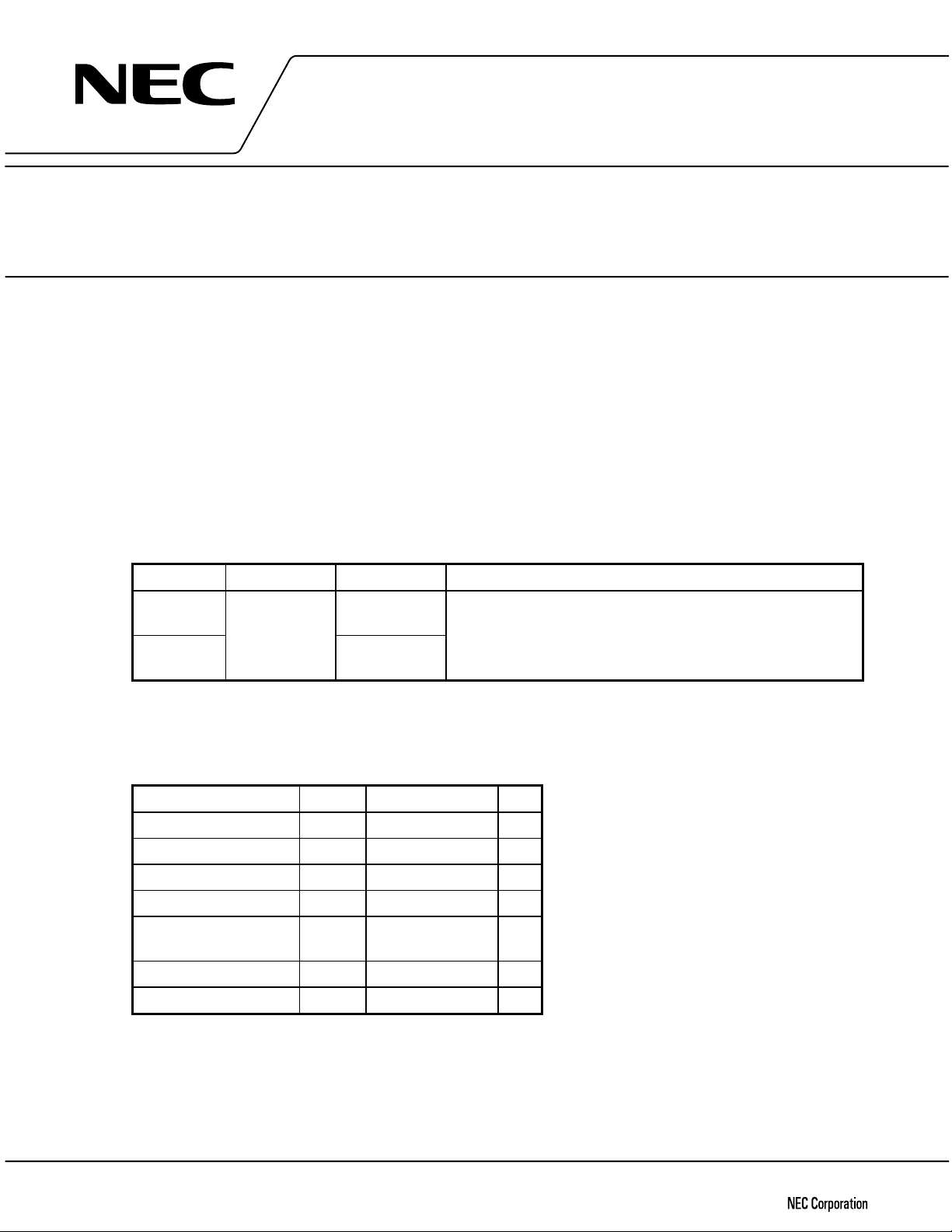
TOTAL POWER DISSIPATION vs.
AMBIENT TEMPERATURE
230
200
100
Total Power Dissipation PT (mW)
16
12
Collector Current IC (mA)
0
8
4
0
2 Elements in total
Per
Element
0 50 100 150
Ambient Temperature TA (°C)
COLLECTOR CURRENT vs.
COLLECTOR TO EMITTER VOLTAGE
0123456
Collector to Emitter Voltage VCE (V)
Free Air
IB = 160 A
IB = 140 A
IB = 120 A
IB = 100 A
IB = 80 A
IB = 60 A
IB = 40 A
IB = 20 A
C)
°°°°
COLLECTOR CURRENT vs.
DC BASE VOLTAGE
20
VCE = 3 V
10
Collector Current IC (mA)
0
0 0.5 1.0
DC Base Voltage VBE (V)
DC CURRENT GAIN vs.
COLLECTOR CURRENT
1 000
µ
µ
µ
µ
µ
µ
µ
µ
100
DC Current Gain hFE
10
0.1 1 10 100
Collector Current IC (mA)
VCE = 3 V
Data Sheet P14552EJ1V0DS00
3
Page 4
µµµµ
PA821TC
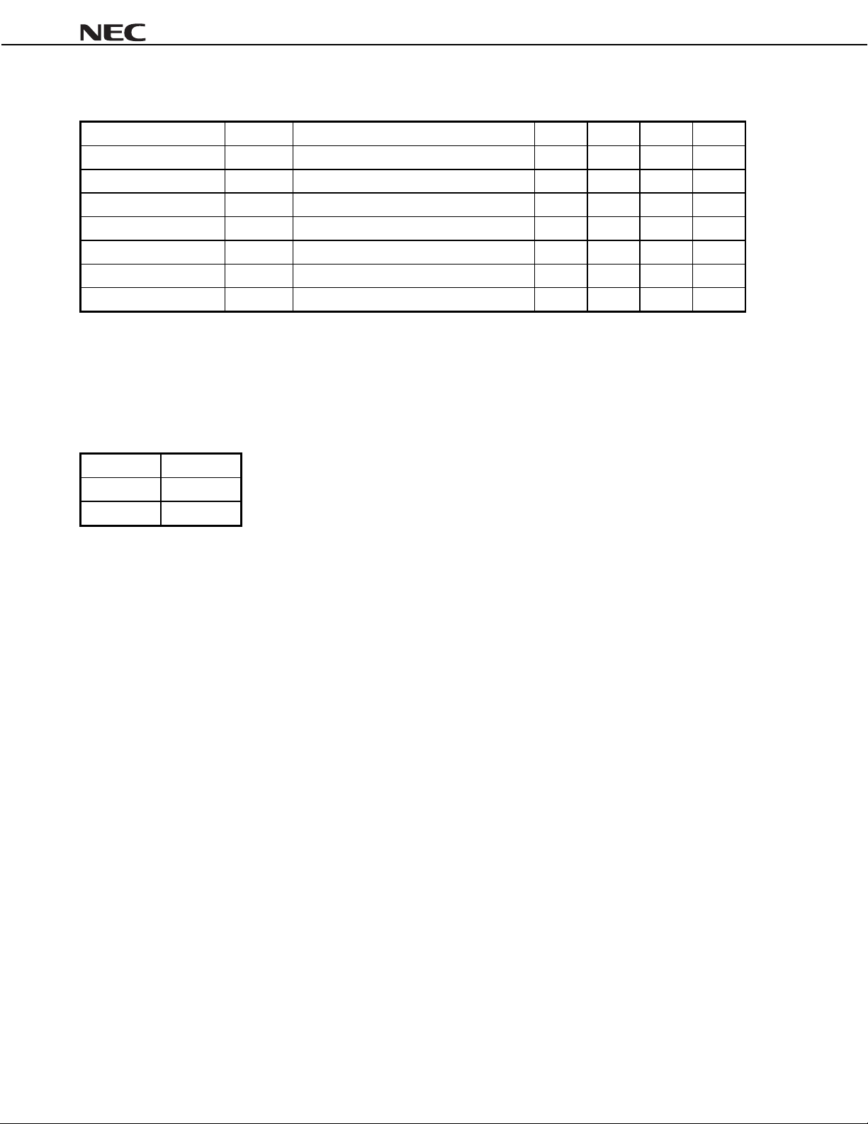
GAIN BANDWIDTH PRODUCT vs.
COLLECTOR CURRENT
7.00
VCE = 3 V
f = 1 GHz
6.00
(GHz)
T
5.00
4.00
3.00
2.00
1.00
Gain Bandwidth Product f
0.00
1 100
Collector Current IC (mA)
NOISE FIGURE vs. COLLECTOR CURRENT
6.00
VCE = 3 V
f = 1 GHz
5.00
4.00
3.00
2.00
Noise Figure NF (dB)
1.00
0.00
1 10 100
Collector Current IC (mA)
INSERTION POWER GAIN vs.
COLLECTOR CURRENT
14.00
VCE = 3 V
f = 1 GHz
12.00
(dB)
2
21e
10.00
8.00
6.00
4.00
Insertion Power Gain S
2.00
1 100
1010
Collector Current IC (mA)
INSERTION POWER GAIN vs. FREQUENCY
25.0
VCE = 3 V
C
= 7 mA
(dB)
2
21e
20.0
I
15.0
10.0
5.0
Insertion Power Gain S
0.0
0.1 1.0 10.0
Frequency f (GHz)
FEEDBACK CAPACITANCE vs.
COLLECTOR TO BASE VOLTAGE
0.800
(pF)
re
0.600
0.400
0.200
Feedback Capacitance C
0.000
1 10 100
Collector to Base Voltage V
4
f = 1 MHz
CB
(V)
Data Sheet P14552EJ1V0DS00
Page 5

S-PARAMETER Q1
CE
= 3 V, IC = 1 mA
V
FREQUENCY S
GHz MAG.ANG.MAG.ANG.MAG.ANG.MAG.ANG.
µµµµ
PA821TC
11
21
S
12
S
22
S
0.1 0.941
0.2 0.913
0.3 0.872
0.4 0.847
0.5 0.807
0.6 0.786
0.7 0.773
0.8 0.763 178.4 1.880 45.8 0.150
0.9 0.753 163.7 1.726 33.9 0.149
1.0 0.748 150.0 1.597 22.5 0.146
1.1 0.749 136.7 1.479 11.6 0.144
1.2 0.740 124.2 1.378 1.1 0.141
1.3 0.748 111.9 1.291
1.4 0.748 100.6 1.216
1.5 0.756 89.6 1.147
1.6 0.757 78.6 1.079
1.7 0.762 68.6 1.025
1.8 0.765 58.2 0.973
1.9 0.770 48.6 0.928
2.0 0.773 38.7 0.882
2.1 0.779 29.2 0.841
2.2 0.776 20.0 0.801
2.3 0.786 11.4 0.767
2.4 0.788 2.0 0.736
2.5 0.791
2.6 0.795
2.7 0.797
2.8 0.797
2.9 0.801
3.0 0.810
VCE = 3 V, IC = 3 mA
FREQUENCY S
GHz MAG.ANG.MAG.ANG.MAG.ANG.MAG.ANG.
30.4 3.863 157.1 0.058 64.5 0.997
−
58.3 3.499 136.9 0.079 52.1 0.947
−
83.6 3.156 118.9 0.103 35.2 0.898
−
107.8 2.833 101.5 0.125 20.1 0.845
−
129.2 2.549 85.9 0.130 8.6 0.793
−
148.3 2.281 71.5 0.142
−
165.3 2.069 58.3 0.146
−
9.2 0.135
−
19.3 0.127
−
29.1 0.124
−
38.8 0.118
−
48.1 0.110
−
57.4 0.105
−
66.3 0.102
−
75.2 0.100
−
83.8 0.098
−
92.6 0.097
−
100.7 0.097
−
109.0 0.102
6.5 0.705
−
15.0 0.677
−
23.6 0.651
−
31.2 0.624
−
39.3 0.602
−
47.0 0.578
−
11
−
116.8 0.111
−
124.7 0.119
−
132.0 0.131
−
139.8 0.139
−
147.3 0.146
−
154.6 0.152
−
21
S
4.6 0.755
−
15.7 0.718
−
25.2 0.693
−
33.2 0.673
−
42.0 0.656
−
49.9 0.644
−
57.4 0.633
−
64.1 0.623
−
71.9 0.614
−
77.6 0.608
−
81.3 0.602
−
86.0 0.597
−
88.5 0.594
−
92.8 0.593
−
93.1 0.587 178.7
−
95.6 0.584 169.7
−
95.0 0.580 160.0
−
95.6 0.577 150.3
−
96.1 0.577 140.6
−
97.8 0.574 130.5
−
99.7 0.577 120.4
−
102.7 0.573 110.3
−
108.3 0.573 100.1
−
113.9 0.572 90.3
−
117.5 0.582 80.2
−
12
S
13.0
−
25.8
−
37.2
−
47.7
−
56.4
−
64.9
−
72.9
−
81.2
−
88.6
−
96.4
−
104.8
−
112.6
−
120.4
−
128.6
−
137.1
−
145.6
−
154.5
−
163.3
−
172.3
−
22
S
0.1 0.869
0.2 0.794
0.3 0.737
0.4 0.695
0.5 0.669
0.6 0.652
0.7 0.641 172.0 3.789 50.9 0.103
0.8 0.636 157.8 3.375 39.8 0.108
0.9 0.634 144.5 3.030 29.4 0.110
1.0 0.634 132.1 2.760 19.2 0.108
1.1 0.637 120.4 2.538 9.3 0.111
1.2 0.638 108.9 2.341
1.3 0.643 98.6 2.178
1.4 0.647 88.3 2.036
1.5 0.654 78.3 1.917
1.6 0.659 68.6 1.804
1.7 0.665 59.2 1.700
1.8 0.673 49.7 1.615
1.9 0.679 40.8 1.533
2.0 0.684 31.6 1.458
2.1 0.689 23.0 1.393
2.2 0.695 14.5 1.329
2.3 0.704 6.1 1.274
2.4 0.709
2.5 0.713
2.6 0.720
2.7 0.725
2.8 0.734
2.9 0.737
3.0 0.744
42.8 9.904 149.2 0.038 52.2 0.945
−
78.9 8.266 125.9 0.070 45.7 0.819
−
108.3 6.914 106.6 0.088 30.5 0.711
−
133.8 5.786 89.7 0.087 16.2 0.623
−
154.6 4.961 75.5 0.103 5.7 0.553
−
172.5 4.274 62.6 0.101
−
0.1 0.114
−
9.4 0.116
−
18.6 0.114
−
27.9 0.118
−
36.9 0.120
−
45.7 0.123
−
54.7 0.127
−
63.1 0.130
−
71.8 0.137
−
80.2 0.140
−
88.7 0.146
−
96.8 0.152
2.2 1.220
−
10.4 1.172
−
18.4 1.130
−
26.6 1.083
−
34.4 1.040
−
42.2 1.010
−
49.8 0.974
−
−
105.1 0.157
−
112.9 0.165
−
121.0 0.173
−
128.8 0.181
−
136.8 0.189
−
144.4 0.197
−
152.1 0.206
−
−
−
−
−
0.4 0.506
−
10.3 0.470
−
14.9 0.440
−
22.1 0.417
−
26.9 0.397
−
31.4 0.386
−
36.6 0.372
−
40.6 0.362
−
45.4 0.350
−
49.6 0.343
−
54.4 0.335
−
58.0 0.330
−
62.5 0.325
−
67.3 0.319 179.7
−
70.3 0.318 170.8
−
75.8 0.313 161.6
−
79.9 0.308 151.7
−
85.2 0.306 141.8
−
89.9 0.305 132.4
−
94.8 0.299 121.2
−
99.8 0.304 110.7
−
105.7 0.307 100.5
−
111.1 0.308 90.0
−
116.8 0.309 79.6
−
121.9 0.317 68.9
−
−
−
−
−
−
106.7
−
114.0
−
121.6
−
129.4
−
136.6
−
145.7
−
153.7
−
162.4
−
171.0
−
21.8
38.9
52.4
62.4
71.2
78.2
85.7
92.3
99.5
Data Sheet P14552EJ1V0DS00
5
Page 6

VCE = 3 V, IC = 5 mA
FREQUENCY S
11
GHz MAG.ANG.MAG.ANG.MAG.ANG.MAG.ANG.
21
S
12
S
S
µµµµ
PA821TC
22
0.1 0.795
0.2 0.713
0.3 0.656
0.4 0.625
0.5 0.603
50.7 14.193 144.1 0.042 40.1 0.913
−
93.1 11.180 118.7 0.061 45.2 0.735
−
123.6 8.924 99.5 0.071 28.4 0.601
−
147.9 7.214 83.6 0.079 16.9 0.501
−
166.9 6.066 70.3 0.085 14.3 0.437
−
0.6 0.593 175.8 5.156 58.3 0.087 5.1 0.392
0.7 0.588 161.3 4.500 47.3 0.091
0.8 0.586 147.7 3.990 37.1 0.091
0.9 0.591 135.5 3.580 27.1 0.098
1.0 0.590 123.9 3.247 17.5 0.101
1.1 0.598 112.9 2.973 8.1 0.105
1.2 0.599 102.6 2.741
1.3 0.607 92.5 2.540
1.4 0.611 82.4 2.370
1.5 0.618 73.0 2.227
1.6 0.625 63.7 2.093
1.7 0.631 54.8 1.973
1.8 0.639 45.7 1.868
1.9 0.645 37.1 1.781
2.0 0.649 28.4 1.688
2.1 0.654 19.7 1.613
2.2 0.658 11.5 1.535
2.3 0.668 3.5 1.475
2.4 0.676
2.5 0.679
2.6 0.686
2.7 0.688
2.8 0.705
2.9 0.716
3.0 0.722
4.8 1.413
−
12.7 1.357
−
20.6 1.303
−
27.8 1.256
−
35.0 1.210
−
43.3 1.169
−
50.9 1.133
−
1.2 0.108
−
10.1 0.114
−
19.1 0.119
−
27.8 0.124
−
36.8 0.131
−
45.1 0.134
−
53.8 0.141
−
62.0 0.146
−
70.6 0.155
−
79.0 0.161
−
87.2 0.168
−
95.2 0.174
−
103.3 0.182
−
111.3 0.192
−
119.4 0.201
−
127.3 0.211
−
134.9 0.203
−
142.6 0.210
−
149.7 0.220
−
3.8 0.355
−
7.2 0.328
−
10.1 0.310
−
16.3 0.292
−
20.4 0.277
−
24.9 0.264
−
30.3 0.259
−
34.6 0.250
−
40.1 0.241
−
45.2 0.233
−
49.8 0.230
−
54.6 0.223
−
60.4 0.219 171.6
−
66.1 0.215 162.5
−
72.0 0.211 152.9
−
76.9 0.208 142.9
−
81.6 0.206 131.2
−
88.0 0.206 121.1
−
94.5 0.203 109.4
−
100.3 0.206 99.1
−
108.8 0.209 88.7
−
116.3 0.219 77.2
−
120.4 0.221 65.3
−
125.2 0.230 54.7
−
VCE = 3 V, IC = 7 mA
FREQUENCY S
11
GHz MAG.ANG.MAG.ANG.MAG.ANG.MAG.ANG.
21
S
12
S
S
27.9
−
46.8
−
60.5
−
70.4
−
77.9
−
85.2
−
92.3
−
98.9
−
105.5
−
112.1
−
120.2
−
127.8
−
135.6
−
143.3
−
152.5
−
160.3
−
169.7
−
177.6
−
22
0.1 0.728
0.2 0.646
0.3 0.597
0.4 0.572
0.5 0.571
59.4 17.820 139.6 0.052 34.1 0.894
−
105.6 13.278 113.3 0.054 40.0 0.655
−
135.1 10.194 94.7 0.063 32.2 0.515
−
159.0 8.098 79.7 0.062 23.0 0.425
−
176.6 6.725 67.0 0.072 13.4 0.356
−
0.6 0.563 167.9 5.698 55.6 0.080 10.6 0.319
0.7 0.563 153.9 4.929 45.3 0.079 5.4 0.287
0.8 0.564 141.5 4.353 35.5 0.090
0.9 0.565 129.9 3.907 25.8 0.094
1.0 0.569 119.2 3.527 16.4 0.098
1.1 0.577 108.5 3.235 7.2 0.102
1.2 0.579 98.6 2.977
1.3 0.586 89.0 2.759
1.4 0.593 79.2 2.571
1.5 0.601 70.1 2.411
1.6 0.605 61.2 2.264
1.7 0.612 52.3 2.130
1.8 0.620 43.6 2.014
1.9 0.627 34.9 1.926
2.0 0.631 26.4 1.822
2.1 0.644 18.2 1.735
2.2 0.646 9.8 1.659
2.3 0.654 1.9 1.592
2.4 0.660
2.5 0.663
2.6 0.662
2.7 0.675
2.8 0.690
2.9 0.703
3.0 0.711
6.1 1.525
−
13.8 1.464
−
21.3 1.405
−
28.7 1.352
−
35.8 1.302
−
44.2 1.261
−
51.8 1.221
−
1.6 0.111
−
10.5 0.116
−
19.2 0.123
−
28.0 0.130
−
36.4 0.135
−
44.9 0.144
−
53.3 0.149
−
61.5 0.157
−
69.9 0.164
−
78.0 0.168
−
86.5 0.177
−
94.3 0.185
−
102.4 0.193
−
110.0 0.204
−
117.9 0.213
−
125.9 0.220
−
133.5 0.215
−
141.0 0.221
−
148.8 0.227
−
0.2 0.261
−
4.4 0.244
−
7.5 0.232
−
14.4 0.219
−
19.8 0.206
−
24.4 0.198
−
29.1 0.190
−
34.2 0.184
−
40.4 0.175
−
45.8 0.173
−
51.4 0.166 172.4
−
57.6 0.163 162.2
−
62.2 0.160 152.2
−
69.0 0.156 141.8
−
75.4 0.153 130.0
−
80.9 0.155 117.7
−
87.6 0.157 106.5
−
94.3 0.158 94.9
−
100.4 0.162 84.0
−
108.9 0.167 73.6
−
116.5 0.179 61.6
−
120.2 0.183 50.2
−
126.4 0.195 39.0
−
−
−
−
−
−
−
−
104.0
−
111.3
−
117.4
−
126.0
−
132.8
−
142.0
−
149.4
−
159.1
−
167.5
−
178.3
−
32.6
53.9
66.6
76.4
83.9
90.2
97.4
6
Data Sheet P14552EJ1V0DS00
Page 7

S-PARAMETER Q2
CE
= 3 V, IC = 1 mA
V
FREQUENCY S
GHz MAG.ANG.MAG.ANG.MAG.ANG.MAG.ANG.
µµµµ
PA821TC
11
21
S
12
S
22
S
0.1 0.940
0.2 0.908
0.3 0.876
0.4 0.848
0.5 0.816
0.6 0.793
0.7 0.774
0.8 0.762
0.9 0.758 167.8 1.735 35.3 0.148
1.0 0.750 154.4 1.604 23.9 0.148
1.1 0.749 142.1 1.492 13.3 0.141
1.2 0.746 130.1 1.392 2.9 0.139
1.3 0.751 118.8 1.306
1.4 0.746 107.5 1.231
1.5 0.751 97.2 1.162
1.6 0.755 87.2 1.107
1.7 0.759 77.2 1.051
1.8 0.759 67.5 1.004
1.9 0.763 58.0 0.966
2.0 0.765 48.6 0.915
2.1 0.768 39.7 0.877
2.2 0.767 30.8 0.840
2.3 0.771 22.4 0.808
2.4 0.774 13.4 0.776
2.5 0.780 5.0 0.746
2.6 0.785
2.7 0.787
2.8 0.790
2.9 0.792
3.0 0.795
VCE = 3 V, IC = 3 mA
FREQUENCY S
GHz MAG.ANG.MAG.ANG.MAG.ANG.MAG.ANG.
30.5 3.922 157.0 0.055 52.8 0.994
−
58.7 3.540 136.7 0.080 52.1 0.939
−
83.9 3.181 118.8 0.107 35.6 0.891
−
107.0 2.840 101.5 0.121 18.0 0.838
−
127.6 2.559 86.2 0.135 10.1 0.789
−
146.3 2.289 71.9 0.143
−
163.2 2.075 58.8 0.146
−
178.2 1.889 46.8 0.147
−
7.2 0.135
−
16.9 0.127
−
26.6 0.126
−
36.0 0.119
−
45.3 0.114
−
54.5 0.109
−
63.4 0.108
−
72.1 0.103
−
80.7 0.100
−
89.2 0.105
−
97.4 0.106
−
105.8 0.114
−
113.5 0.120
3.1 0.721
−
11.8 0.693
−
19.4 0.667
−
27.5 0.647
−
35.2 0.626
−
11
−
121.7 0.128
−
129.1 0.140
−
136.4 0.149
−
143.8 0.162
−
150.8 0.176
−
21
S
2.9 0.747
−
14.3 0.713
−
24.0 0.688
−
30.6 0.671
−
39.8 0.655
−
46.9 0.635
−
53.2 0.623
−
61.4 0.613
−
66.3 0.606
−
71.8 0.598
−
77.1 0.591
−
80.6 0.585
−
83.1 0.578
−
86.2 0.574
−
87.0 0.572 176.6
−
89.5 0.562 167.1
−
89.5 0.561 156.9
−
90.5 0.557 146.9
−
90.8 0.553 136.7
−
91.9 0.550 126.3
−
95.2 0.550 115.6
−
97.0 0.548 105.1
−
101.2 0.551 94.6
−
105.3 0.550 83.6
−
110.7 0.551 72.6
−
12
S
13.7
−
26.0
−
37.4
−
47.5
−
56.7
−
65.1
−
73.5
−
81.1
−
89.2
−
97.0
−
105.2
−
112.9
−
121.0
−
129.9
−
138.5
−
146.8
−
155.8
−
164.6
−
173.8
−
22
S
0.1 0.859
0.2 0.803
0.3 0.744
0.4 0.703
0.5 0.687
0.6 0.665
0.7 0.655 176.4 3.678 52.2 0.101
0.8 0.649 162.7 3.300 41.3 0.107
0.9 0.646 150.1 2.967 31.1 0.107
1.0 0.641 138.2 2.717 21.0 0.110
1.1 0.648 126.9 2.500 11.2 0.111
1.2 0.646 116.4 2.317 1.6 0.110
1.3 0.645 106.2 2.155
1.4 0.652 96.4 2.021
1.5 0.662 87.0 1.904
1.6 0.662 77.6 1.797
1.7 0.668 68.5 1.705
1.8 0.670 59.4 1.618
1.9 0.675 50.8 1.551
2.0 0.678 42.2 1.472
2.1 0.686 33.4 1.409
2.2 0.686 25.4 1.348
2.3 0.693 17.1 1.294
2.4 0.698 9.0 1.242
2.5 0.703 1.3 1.200
2.6 0.709
2.7 0.710
2.8 0.717
2.9 0.724
3.0 0.727
41.4 9.530 149.9 0.059 46.3 0.965
−
78.2 7.977 126.6 0.067 42.2 0.836
−
106.9 6.695 107.5 0.088 26.9 0.727
−
131.2 5.614 90.7 0.091 17.2 0.637
−
151.3 4.863 76.4 0.100 7.7 0.568
−
169.1 4.172 63.9 0.101 0.0 0.519
−
7.4 0.113
−
16.6 0.114
−
25.5 0.116
−
34.5 0.120
−
43.5 0.123
−
52.2 0.127
−
60.5 0.130
−
69.2 0.137
−
77.4 0.142
−
86.1 0.147
−
94.2 0.153
−
102.3 0.162
−
110.1 0.169
6.7 1.157
−
14.2 1.123
−
21.9 1.080
−
29.5 1.044
−
37.0 1.009
−
−
118.3 0.178
−
125.6 0.186
−
133.7 0.195
−
141.5 0.204
−
149.4 0.215
−
−
−
−
−
−
8.0 0.480
−
14.3 0.448
−
19.3 0.429
−
24.9 0.410
−
29.8 0.393
−
35.0 0.380
−
40.3 0.371
−
44.3 0.359
−
47.3 0.351
−
51.6 0.341
−
54.8 0.336
−
59.1 0.329
−
64.0 0.324
−
68.8 0.314 172.8
−
73.0 0.305 163.4
−
76.7 0.302 153.5
−
80.8 0.299 142.8
−
85.7 0.293 132.5
−
90.6 0.293 121.8
−
95.8 0.291 110.9
−
101.3 0.291 99.8
−
107.2 0.291 88.4
−
112.5 0.293 77.1
−
118.5 0.298 66.0
−
−
−
−
−
104.2
−
111.7
−
119.2
−
126.7
−
134.5
−
142.6
−
151.1
−
160.0
−
168.6
−
177.8
−
20.7
37.7
51.2
60.7
68.7
76.5
82.4
90.3
97.3
Data Sheet P14552EJ1V0DS00
7
Page 8

µµµµ
PA821TC
VCE = 3 V, IC = 5 mA, Z0 = 50
FREQUENCY S
GHz MAG.ANG.MAG.ANG.MAG.ANG.MAG.ANG.
0.1 0.774
0.2 0.700
0.3 0.657
0.4 0.630
0.5 0.616
0.6 0.601 179.2 5.143 59.3 0.087 7.0 0.397
0.7 0.598 164.7 4.479 48.5 0.088 0.7 0.359
0.8 0.597 152.3 3.984 38.6 0.096
0.9 0.598 140.5 3.571 28.4 0.096
1.0 0.601 129.9 3.240 19.1 0.103
1.1 0.601 119.4 2.971 9.8 0.106
1.2 0.604 109.4 2.745 0.7 0.108
1.3 0.612 100.3 2.554
1.4 0.615 90.8 2.387
1.5 0.622 81.6 2.236
1.6 0.624 73.0 2.115
1.7 0.631 64.5 2.003
1.8 0.636 55.8 1.897
1.9 0.643 47.6 1.809
2.0 0.647 39.1 1.716
2.1 0.653 30.5 1.649
2.2 0.656 22.9 1.574
2.3 0.662 15.0 1.516
2.4 0.668 6.9 1.455
2.5 0.672
2.6 0.681
2.7 0.685
2.8 0.687
2.9 0.695
3.0 0.701
Ω
11
52.0 14.036 144.4 0.035 28.8 0.928
−
93.8 11.057 119.1 0.057 40.7 0.729
−
122.9 8.835 100.1 0.072 31.2 0.602
−
146.9 7.147 84.3 0.076 17.7 0.505
−
165.6 6.011 71.1 0.077 12.2 0.439
−
0.5 1.404
−
8.3 1.352
−
15.9 1.307
−
23.4 1.257
−
30.7 1.226
−
38.0 1.187
−
21
S
8.2 0.113
−
17.0 0.116
−
25.7 0.122
−
34.5 0.129
−
42.8 0.138
−
51.3 0.142
−
59.6 0.147
−
67.9 0.154
−
76.3 0.160
−
84.7 0.169
−
92.6 0.173
−
100.6 0.184
−
108.5 0.191
−
116.6 0.199
−
124.0 0.207
−
131.8 0.214
−
139.6 0.224
−
147.1 0.233
−
12
S
6.8 0.329
−
9.8 0.311
−
14.3 0.291
−
18.6 0.278
−
23.8 0.267
−
27.9 0.254
−
32.9 0.245
−
36.1 0.236
−
41.3 0.227
−
46.9 0.220
−
51.7 0.213
−
57.3 0.203 176.6
−
62.0 0.198 166.9
−
68.6 0.192 156.5
−
74.0 0.186 145.4
−
79.2 0.183 133.9
−
85.0 0.181 122.6
−
90.8 0.177 110.3
−
95.5 0.181 98.8
−
102.5 0.182 86.5
−
108.9 0.186 75.3
−
114.6 0.189 62.9
−
120.8 0.196 51.6
−
S
22
27.8
−
45.7
−
59.2
−
69.4
−
76.1
−
83.6
−
88.8
−
95.9
−
102.9
−
109.3
−
116.6
−
123.4
−
131.2
−
138.8
−
147.5
−
156.5
−
165.4
−
173.8
−
VCE = 3 V, IC = 7 mA
FREQUENCY S
GHz MAG.ANG.MAG.ANG.MAG.ANG.MAG.ANG.
0.1 0.716
0.2 0.659
0.3 0.609
0.4 0.583
0.5 0.575
0.6 0.570 173.1 5.602 57.4 0.079 12.1 0.332
0.7 0.569 159.9 4.892 47.2 0.083 5.2 0.297
0.8 0.569 148.0 4.323 37.3 0.089
0.9 0.571 136.7 3.873 27.8 0.095
1.0 0.574 126.6 3.507 18.5 0.099
1.1 0.576 116.2 3.224 9.3 0.108
1.2 0.581 106.6 2.969 0.3 0.114
1.3 0.589 97.8 2.765
1.4 0.590 88.6 2.581
1.5 0.599 79.8 2.423
1.6 0.601 71.2 2.284
1.7 0.605 62.7 2.146
1.8 0.612 54.4 2.044
1.9 0.620 46.1 1.948
2.0 0.623 38.2 1.857
2.1 0.632 29.8 1.770
2.2 0.636 22.2 1.695
2.3 0.638 13.9 1.629
2.4 0.648 6.1 1.565
2.5 0.653
2.6 0.660
2.7 0.665
2.8 0.673
2.9 0.676
3.0 0.682
11
54.8 16.827 141.3 0.073 54.7 0.897
−
100.9 12.791 115.4 0.050 37.9 0.674
−
131.4 9.920 96.6 0.064 28.4 0.543
−
154.2 7.925 81.4 0.068 22.6 0.446
−
171.7 6.631 68.9 0.073 17.5 0.373
−
1.4 1.510
−
9.1 1.455
−
16.4 1.408
−
23.9 1.356
−
31.3 1.323
−
38.4 1.279
−
21
S
8.3 0.119
−
16.9 0.122
−
25.6 0.131
−
34.0 0.139
−
42.5 0.146
−
51.0 0.151
−
59.0 0.160
−
67.4 0.168
−
75.3 0.172
−
83.7 0.183
−
91.5 0.188
−
99.7 0.197
−
107.5 0.205
−
115.4 0.214
−
123.1 0.223
−
130.8 0.230
−
138.4 0.236
−
145.9 0.243
−
12
S
0.5 0.270
−
3.9 0.250
−
8.7 0.234
−
14.2 0.222
−
19.6 0.209
−
23.3 0.197
−
27.9 0.187
−
33.9 0.178
−
39.4 0.170
−
45.0 0.163
−
49.4 0.153 179.3
−
56.2 0.149 167.7
−
61.4 0.139 158.0
−
67.6 0.134 146.2
−
73.4 0.130 134.0
−
79.7 0.129 121.3
−
85.2 0.125 109.2
−
91.3 0.127 95.9
−
97.2 0.130 82.3
−
103.4 0.134 68.9
−
110.5 0.142 56.9
−
116.8 0.145 44.7
−
123.1 0.156 34.8
−
S
22
28.5
−
51.3
−
64.6
−
74.4
−
81.3
−
88.5
−
93.9
−
100.3
−
107.7
−
113.3
−
122.4
−
128.4
−
136.5
−
145.1
−
153.4
−
162.1
−
172.0
−
8
Data Sheet P14552EJ1V0DS00
Page 9

PACKAGE DIMENSIONS
FLAT-LEAD 6 PIN THIN-TYPE ULTRA SUPER MINIMOLD (UNIT: mm)
(Top View)
B1
E2
B2
µµµµ
PA821TC
0.96
1.50±0.1
0.480.48
0.55±0.05
1.50±0.1
1.10±0.1
123
81
+0.1
–0.05
0.20
654
+0.1
–0.05
0.11
PIN CONNECTIONS
1. Collector (Q1)
2. Emitter (Q1)
3. Collector (Q2)
6
Q1 Q2
1
C1
2
E1
4
5
3
C2
4. Base (Q2)
5. Emitter (Q2)
6. Base (Q1)
Data Sheet P14552EJ1V0DS00
9
Page 10

[MEMO]
µµµµ
PA821TC
10
Data Sheet P14552EJ1V0DS00
Page 11

[MEMO]
µµµµ
PA821TC
Data Sheet P14552EJ1V0DS00
11
Page 12

µµµµ
PA821TC
• The information in this document is subject to change without notice. Before using this document, please
confirm that this is the latest version.
• No part of this document may be copied or reproduced in any form or by any means without the prior written
consent of NEC Corporation. NEC Corporation assumes no responsibility for any errors which may appear in
this document.
• NEC Corporation does not assume any liability for infringement of patents, copyrights or other intellectual property
rights of third parties by or arising from use of a device described herein or any other liability arising from use
of such device. No license, either express, implied or otherwise, is granted under any patents, copyrights or other
intellectual property rights of NEC Corporation or others.
• Descriptions of circuits, software, and other related information in this document are provided for illustrative
purposes in semiconductor product operation and application examples. The incorporation of these circuits,
software, and information in the design of the customer's equipment shall be done under the full responsibility
of the customer. NEC Corporation assumes no responsibility for any losses incurred by the customer or third
parties arising from the use of these circuits, software, and information.
• While NEC Corporation has been making continuous effort to enhance the reliability of its semiconductor devices,
the possibility of defects cannot be eliminated entirely. To minimize risks of damage or injury to persons or
property arising from a defect in an NEC semiconductor device, customers must incorporate sufficient safety
measures in its design, such as redundancy, fire-containment, and anti-failure features.
• NEC devices are classified into the following three quality grades:
"Standard", "Special", and "Specific". The Specific quality grade applies only to devices developed based on a
customer designated "quality assurance program" for a specific application. The recommended applications of
a device depend on its quality grade, as indicated below. Customers must check the quality grade of each device
before using it in a particular application.
Standard: Computers, office equipment, communications equipment, test and measurement equipment,
audio and visual equipment, home electronic appliances, machine tools, personal electronic
equipment and industrial robots
Special: Transportation equipment (automobiles, trains, ships, etc.), traffic control systems, anti-disaster
systems, anti-crime systems, safety equipment and medical equipment (not specifically designed
for life support)
Specific: Aircraft, aerospace equipment, submersible repeaters, nuclear reactor control systems, life
support systems or medical equipment for life support, etc.
The quality grade of NEC devices is "Standard" unless otherwise specified in NEC's Data Sheets or Data Books.
If customers intend to use NEC devices for applications other than those specified for Standard quality grade,
they should contact an NEC sales representative in advance.
M7 98. 8
 Loading...