

Page 1
uP7701
A
3A Ultra Low Dropout Linear Regulator
General Description
The uP7701 is a 3A ultra low dropout linear regulator
specifically designed for motherboard,notebook and graphic
card applications. This device works with dual supplies, a
control input for the control circuitry and a power input as
low as 1.0V for providing current to output. The uP7701
delivers high-current and ultra-low-drop output voltage as
low as 0.8V for applications where V
is very close to
OUT
VIN.
The uP7701 features comprehensive control and protection
functions: a power on reset (POR) circuit for monitoring
both control and power inputs for proper operation; an EN
input for enabling or disabling the device, a power OK with
time delay for indicating the output voltage status, a
foldback current limit function, and a thermal shutdown
function.
The uP7701 is available in PSOP-8 package with very low
thermal resistance.
pplications
Desktop PCs, Notebooks, and Workstations
Graphic Cards
Low Voltage Logic Supplies
Microprocessor and Chipset Supplies
Split Plane Microprocessor Supplies
Advanced Graphics Cards Supplies
SoundCards and Auxiliary Power Supplies
SMPS Post Regulators
Features
Works with 1.0V~5.5V V
Adjustable Output Voltage, Down to 0.8V
1.5% Initial Accuracy
Excellent Line and Load Regulation
3A Guaranteed Output Current
IN
300mV @ 3A Dropout Voltage
Very Low On-Resistance
100m
V
OUT
Low Reverse Leakage (Output to Input )
V
OUT
Fast Transient Response
Low External Component Count
Low Cost and Easy to Use
Enable Pin
Over Current and Over Temperature Protection
ΩΩ
Ω typical
ΩΩ
Pull Low Resistance when Disabled
Power OK Signal
Ordering Information
rebmuNredrOepyTegakcaPkrameR
8U1077Pu8-POSP
Note: uPI products are compatible with the current IPC/
JEDEC J-STD-020 and RoHS requirements. They are 100%
matte tin (Sn) plating and suitable for use in SnPb or Pbfree soldering processes.
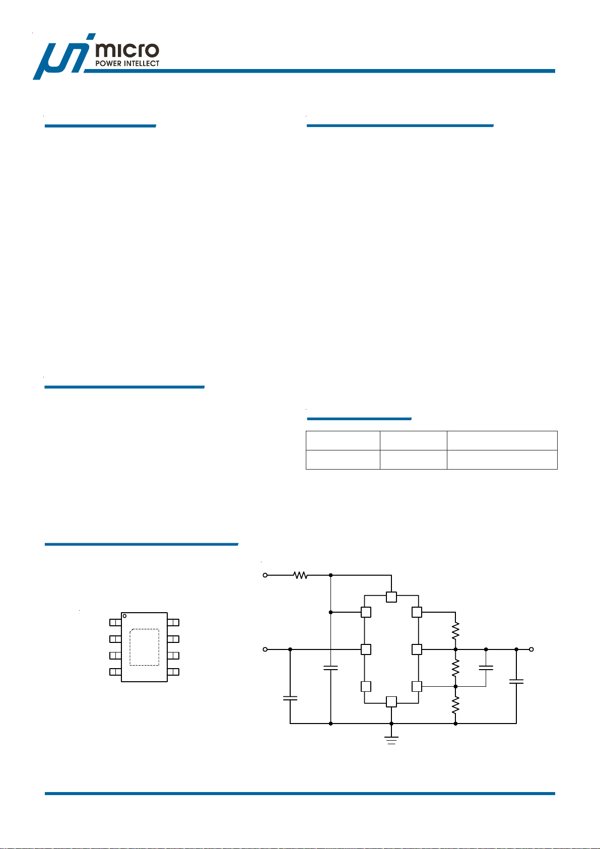
Pin Configuration & Typical Application Circuit
1
2
EN
3
VIN
CNTL
uPI Semiconductor Corp., http://www.upi-semi.com
Rev. 00, 2007, April
45
GND
uP7701
8
GNDPOK
7
FB
6
VOUT
NC
5VCC
V
IN
R4
10R
C2
4.7uF
C1
1uF
EN
NC
CNTL
2
3
5
4
8
uP7701
GND
POK
1
R3
VOUTVIN
6
FB
7
10K
R2
12.5K
R1
10K
C4
option
V
OUT
C3
10uF
1
Page 2
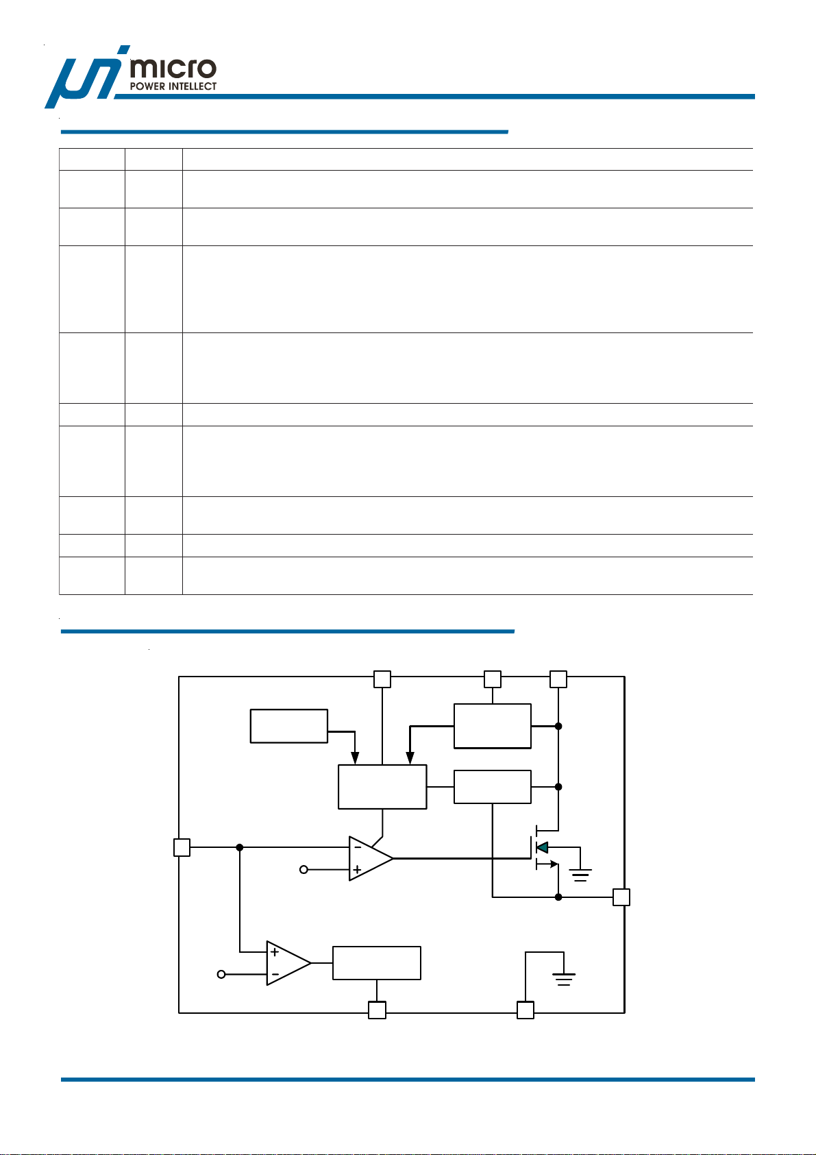
.oNniPemaNnoitcnuFniP
n
1KOP
2NE
3NIV
4LTNC
5CN
6TUOV
7BF
8DNG
desopxE
daP
uP7701
Functional Pin Descriptio
.noitacidnIKOrewoP Vecnoecnadepmihgihtessidnatuptuoniard-neponasinipsihT
.egatlovgnitarstifo%29sehcaer
.tupnIelbanE tnerructnecseiuqehtgnicuder,fforotalugerehtsnrutV4.0wolebnipsihtgnilluP
.eulavgnitarepostifonoitcarfaot
.egatloVtupnI .niptuptuoehtottnerrucylppustahtecivedrewopehtottupniniardehtsisihT
V.nipsihtta
NI
Vnahtrehgihdecrofebtonnac
LTNC
.egatlovtuptuoehtelbasiddnadereggirt
.tiucriClortnoCroftupnIylppuS dnayrtiucriclortnocehtotegatlovsaibsedivorpnipsihT
Vnahtsselondna,egatlov
.NIM_LTNC
detcennoCyllanretnItoN
.egatloVtuptuO ehtnehwstsixeecnatsiserwolllupA.ecivedehtfotuptuorewopsinipsihT
.TUOVnostneisnarttnerrucfostceffeehtecuderotdednemmocer
.egatloVkcabdeeF morfredividrotsiserA.reifilpmarorreehtottupnignitrevniehtsinipsihT
VsaegatlovnoitalugerehttesotdesusiDNGottuptuoeht
TUO
)V(1R/)2R+1R(x8.0=
.dnuorG
DNG
.dnuorG deredlosebdluohsdnahtapnoitapissidrewoptnanimodehtstcadapdesopxeehT
ehtnidebircsedsasdapBCPngisedllewot .retpahCsnoitamrofnInoitacilppA
TUO
ehttneverponipsihtotesolcyllacisyhpdecalpebdluohsRSEwolhtiwsroticapacklubegraL
dednemmocersiroticapaccimarecFu7.4A.tneisnartdaolegralgnirudgnippordmorfliartupni
eslafebyamnoitcnuftimiltnerrucehtesiwrehto
.
VehtotdenoitroporpsitnerructuptuofoytilibapacgnivirdehT.rotsisnartssapehtrofrevird
LTNC
tuptuoehtnahtretaergV5.1tsaeltaebtsumnipsihtnoegatloveht,etalugerotecivedehtroF
egralotesnopsertneisnartetauqedaniatniamoT.nipNEehtwolgnillupybdelbasidsiecived
erasroticapaccimarecFu01htiwroticapaccitylortcelelAFu0001foeulavlacipyt,egnahcdaol
FB
Functional Block Diagram
CNTLEN
2
Thermal Limit
Softstart &
Control Logic
7
0.8V
Delay
92% V
REF
1
POK GND
4
Power On
Reset
Current Limit
VIN
3
6
VOUT
8
uPI Semiconductor Corp., http://www.upi-semi.com
Rev. 00, 2007, April
2
Page 3
uP7701
Functional Description
Definitions
Some important terminologies for LDO are specified below.
Dropout Voltage
The input/output voltage differential at which the regulator
output no longer maintains regulation against further
reductions in input voltage. Measured when the output drops
2% below its nominal value. Dropout voltage is affected by
junction temperature, load current and minimum input
supply requirements.
Line Regulation
The change in output voltage for a change in input voltage.
The measurement is made under conditions of low
dissipation or by using pulse techniques such that average
chip temperature is not significantly affected.
Load Regulation
The change in output voltage for a change in load current
at constant chip temperature. The measurement is made
under conditions of low dissipation or by using pulse
techniques such that average chip temperature is not
significantly affected.
Maximum Power Dissipation
Output Voltage Programming
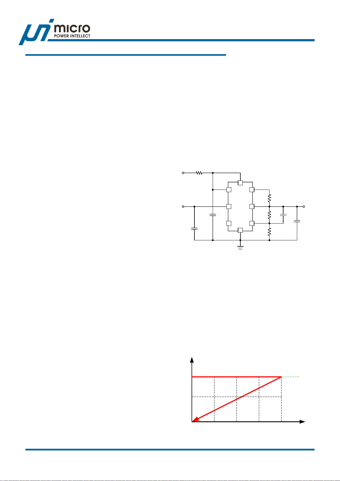
Figure 1 shows a typical application of 2.5V to 1.8V
conversion with a 5.0V control supply. The output voltage
is sensed through a voltage divider and regulated to internal
reference voltage V
. The output voltage is programmed
REF
as:
V
= V
OUT
x (R1+R2) / R1 = 0.8V x (22.5k/10k) = 1.8V
REF
It’s recommended to maintain 50-100uA through the output
divider network for a tight load and line regulation. The
internal voltage reference is V
= 0.8V with 1.5% initial
REF
accuracy. This commands the use of 0.5% or better
accuracy resistors to build a precision power supply.
5VCC
R4
10R
V
IN
C1
1uF
C2
4.7uF
EN
NC
CNTL
2
3
5
4
POK
1
R3
10K
VOUTVIN
6
uP7701
FB
7
8
GND
R2
12.5K
R1
10K
C4
option
V
OUT
C3
10uF
The maximum total device dissipation for which the
regulator will operate within specifications.
Quiescent Bias Current
Current which is used to operate the regulator chip and is
not delivered to the load.
The quiescent current IQ is defined as the supply current
used by the regulator itself that does not pass into the
load. It typically includes all bias currents required by the
LDO and any drive current for the pass transistor.
Initialization
The uP7701 automatically initiates upon the receipt of
supply voltage and power voltage. A power on reset circuit
continuously monitors VIN and CNTL pins voltages with
rising threshold levels of 0.6V and 2.7V respectively.
Chip Enable and Soft Start
The uP7701 features an enable pin for enable/disable
control of the chip. Pulling VEN lower than 0.8V disables
the chip and reduces its quiescent current down to 12uA.
When disabled, an internal MOSFET of 90Ω R
DS(ON)
turns
on to pull output voltage to ground. Pulling VEN higher than
1.6V enables the output voltage, providing POR is
recognized. The uP7701 features soft start function that
limits inrush current for charging the output capacitors. The
soft start time is typically 5ms.
Figure 1. Typical application of 2.5V to 1.8V conversion
with a 5.0V control supply
Over Current Protection
The uP7701 features a foldback over current protection
function as shown in Figure 2. The current limit threshold
level is proportinal to V
V
= V
OUT
, where V
NOM
NOM
OUT/VNOM
is the target output voltage. If the
and is typically 4A when
output continuously demands more current than the
maximum current, output voltage will eventually drops below
its nominal value. This, in turns, will lower its OCP threshold
level. This will limit power dissipation in the device when
over current limit happens. The power dissipation is near
zero when the output is short circuited to ground.
V
NOM
1V
P
C
S
Output Voltage (V)
3A2A1A
4A
Output Current (A)
Figure 2. Current Limit Behavior
uPI Semiconductor Corp., http://www.upi-semi.com
Rev. 00, 2007, April
3
Page 4
uP7701
A
g
n
bsolute Maximum Ratin
Control Input Voltage V
Power Input Voltage V
Other Pins --------------------------------------------------------------------------------------------------------------- -0.3V to (V
(Note 1) ------------------------------------------------------------------------------------------------- -0.3V to +6V
CNTL
-------------------------------------------------------------------------------------------------------------------- -0.3V to +6V
IN
+ 0.3V)
CNTL
Storage Temperature Range ----------------------------------------------------------------------------------------------------------- -65OC to +150OC
Junction Temperature ------------------------------------------------------------------------------------------------------------------------------------ 150OC
Lead Temperature (Soldering, 10 sec) ------------------------------------------------------------------------------------------------------------ 260OC
ESD Rating (Note 2)
HBM (Human Body Mode) --------------------------------------------------------------------------------------------------------------------- 2kV
MM (Machine Mode) ----------------------------------------------------------------------------------------------------------------------------- 200V
Thermal Informatio
Package Thermal Resistance (Note 3)
PSOP-8 θJA ---------------------------------------------------------------------------------------------------------------------------------- 52°C/W
PSOP-8 θJC ---------------------------------------------------------------------------------------------------------------------------------- 15°C/W
Power Dissipation, PD @ T
= 25°C
A
PSOP-8 ------------------------------------------------------------------------------------------------------------------------------------------- 1.9W
Recommended Operation Conditions
Operating Junction Temperature Range (Note 4) ------------------------------------------------------------------------ -40°C to +125°C
Operating Ambient Temperature Range -------------------------------------------------------------------------------------- -40°C to +85°C
Supply Input Voltage, V
Power Input Voltage, V
------------------------------------------------------------------------------------------------------------ +4.5V to +5.5V
CNTL
------------------------------------------------------------------------------------------------------------ +1.0V to V
IN
CNTL
(V
= 5V, TA = 25OC, unless otherwise specified)
CNTL
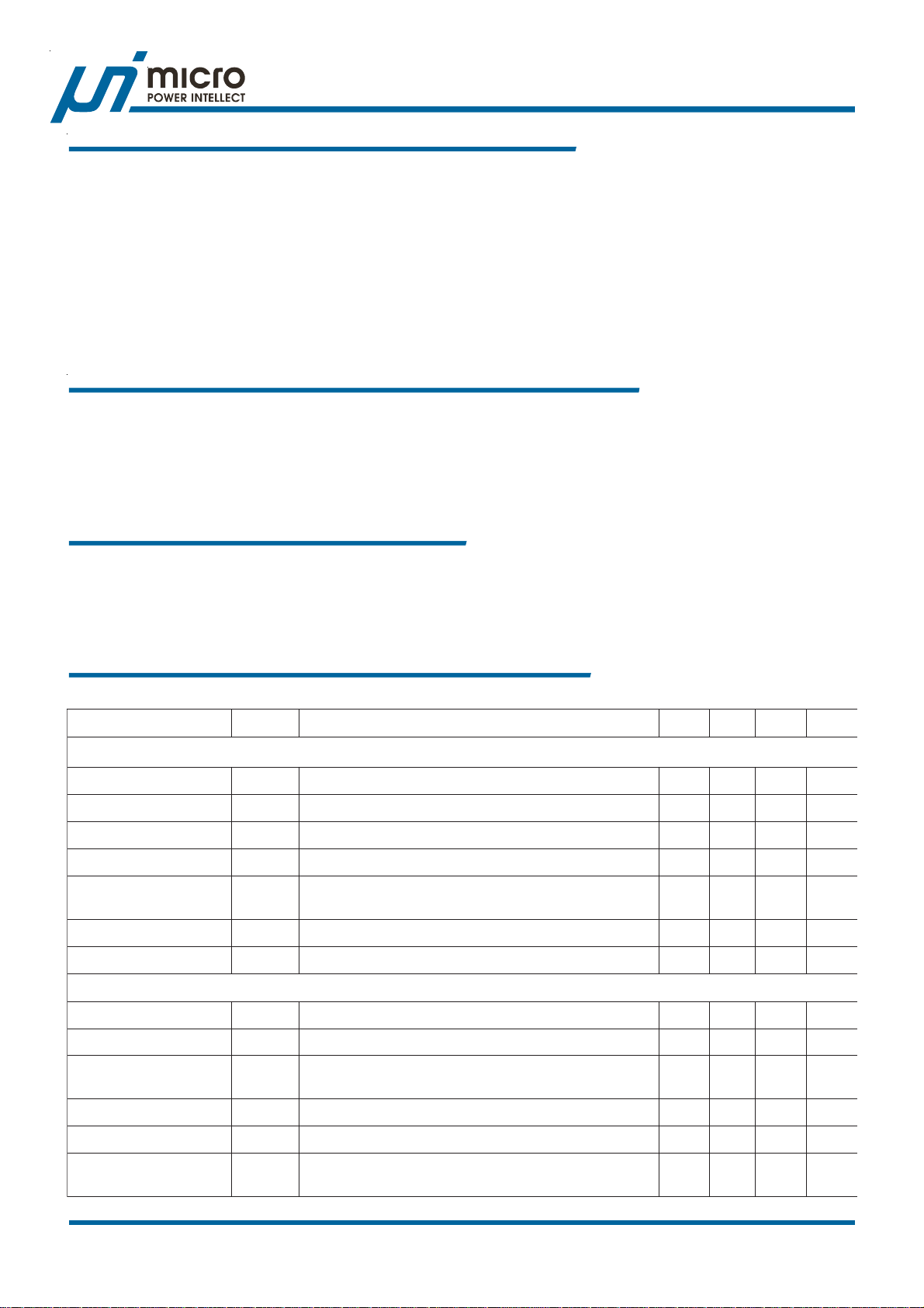
retemaraPlobmySsnoitidnoCtseTniMpyTxaMstinU
egatloVtupnIylppuS
egatloVtupnIlortnoCV
dlohserhTROPV
siseretsyHROPV
egatloVtupnIrewoPV
nitnerruCtupnIlortnoC
nwodtuhS
I
tnerruCtupnIlortnoCI
tnerruCtnecseiuQI
V
LTNC
HTRLTNC
SYHLTNC
V
NI
V
DS_LTNC
V
LTNC
V
Q
egatloVkcabdeeF
egatloVecnerefeRV
tnerruCtupnIkcabdeeFI
V
NI
V
LTNC
noitalugeReniLV
noitalugeReniLV
noitalugeRdaoLV
revonoitalugeRdaoL
erutarepmeT
V
V
FER
BF
)ENIL(FER
V
)LTNC(FER
)DAOL(FER
)LATOT(FER
Electrical Characteristics
V=
TUO
FER
V=
TUO
FER
V=
LTNC
NI
V=
LTNC
NI
V=
LTNC
NI
V=
LTNC
NI
V<V0.1
NI
FER
V<V0.3
I<Am0
TUO
I<Am0
TUO
O
T<C
04-
J
I,V0.5=
TUO
V=
NE
V=
NE
V=
NE
V,V0.5<
LTNC
V,V0.5<
V,A3<
LTNC
V,A2<
LTNC
O
521<
V,A0=
V0=--0204Au
NE
I,V0.5=
I,V0.5=
I,V0.5=
V=
LTNC
NI
V=
NI
V=
NI
V,A0=
TUO
TUO
TUO
NE
I,V2.1=
TUO
V=
NE
V=
NE
ngisedyb,C
V=
TUO
FER
V,A0=
V=
TUO
FER
V.A0=
V=
TUO
FER
I,V0.5=
V.A0=
TUO
V.A0=
TUO
V,V0.5=
V,V0.5=
=
TUO
V=
FER
V=
TUO
FER
V=
TUO
,
FER
0.3--5.5V
--7.29.2V
--2.0--V
0.1--V
V
LTNC
--0.15.1Am
--0.15.1Am
887.08.0218.0V
--02--An
--1.03.0V/%
--1.03.0V/%
--5.00.1A/%
--0.12%
uPI Semiconductor Corp., http://www.upi-semi.com
Rev. 00, 2007, April
4
Page 5
uP7701
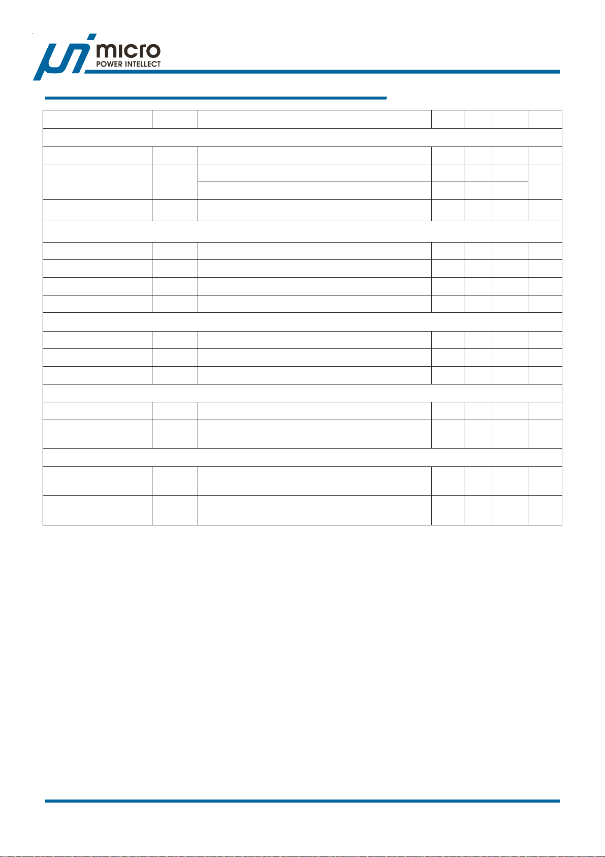
Electrical Characteristics
retemaraPlobmySsnoitidnoCtseTniMpyTxaMstinU
V(egatloVkcabdeeF
ecnatsiseRnOR
egatloVtuoporDV
V
TUO
V=
NIFER
ecnatsiseRwoLlluPV
)LTNC
I
)NO(SD
TUO
I
TUO
PORD
I
TUO
LTNC
V,Am001=
V,A2=
LTNC
V,A3=
LTNC
V=
NI
V=
LTNC
NE
V=
NE
V=
NE
V,V0.5=
NE
V,V0.5=
V,V0.5=
V,V0.5=
TUO
TUO
V6.1=--001021mΩ
TUO
ngisedyb,V6.1=--002042
ngisedyb,V6.1=003063
ngisedyb,V0=--09-- Ω
Vm
elbanE
leveLhgiHelbanEV
leveLwoLelbasiDV
tnerruCecruoSNEI
ecnadepmItupnINEZ
NE
DS
NE
NE
V
NE
V,V0=
V0.5=--2102Au
LTNC
----6.1V
4.0----V
--56--KΩ
KORWP
dlohserhTKOrewoPBFV
siseretsyHKOrewoPV
I
HTKOP
I
SYHKOP
emiTyaleDKOPVmorF
V,A0=
TUO
V,A0=
TUO
TUO
V=
LTNC
LTNC
V=
NI
NE
V=
V=
NI
NE
V%29>
MON
V,V0.5=
V=
TUO
FER
V,V0.5=
V=
TUO
FER
--29--%
--8 --%
gnisirKOPot--1--sm
noitcetorPtnerrucrevO
leveLdlohserhTPCOI
tiucriCtrohStuptuO
tnerruC
PCO
I
CS
V
V=
LTNC
V
LTNC
V=
NI
NE
V=
V=
NI
NE
V,V0.5=
V=
TUO
FER
V,V0.5=
=V0--001--Am
TUO
5.3----A
noitcetorPlamrehT
nwodtuhSlamrehT
erutarepmeT
nwodtuhSlamrehT
siseretsyH
T
DS
T
I
I
SYHDS
V,A0=
TUO
V,A0=
TUO
V=
LTNC
LTNC
V=
NI
NE
V=
V=
NI
NE
V,V0.5=
V=
TUO
FER
V,V0.5=
V=
TUO
FER
--071--
--03--
O
O
Note 1. Stresses listed as the above “Absolute Maximum Ratings” may cause permanent damage to the device.
These are for stress ratings. Functional operation of the device at these or any other conditions beyond those
indicated in the operational sections of the specifications is not implied. Exposure to absolute maximum
rating conditions for extended periods may remain possibility to affect device reliability.
Note 2. Devices are ESD sensitive. Handling precaution recommended.
Note 3. θ
is measured in the natural convection at T
JA
= 25°C on a low effective thermal conductivity test board of
A
JEDEC 51-3 thermal measurement standard.
Note 4. The device is not guaranteed to function outside its operating conditions.
C
C
uPI Semiconductor Corp., http://www.upi-semi.com
Rev. 00, 2007, April
5
Page 6
uP7701
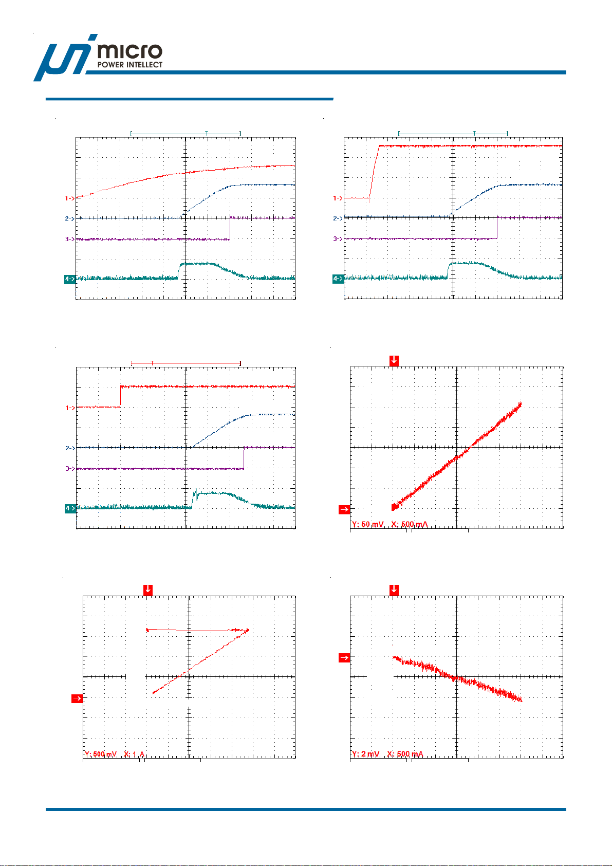
Typical Operation Characteristics
V
=5V, VIN = 3.3V, C
CNTL
Power On from V
1ms/Div
= 1000uF, No Load.
OUT
Turn On from EN
IN
V
POK (5V/Div)
VEN (5V/Div)
V
OUT
VIN (2V/Div)
(1V/Div)
OUT
IIN (1A/Div)
(1V/Div)
Power On from V
CNTL
V
POK (5V/Div)
CNTL
V
1ms/Div
V
=5V, VIN = 3.3V, C
CNTL
= 1000uF, No Load.
OUT
Dropout Voltage vs. Output Current
300mV
(2V/Div)
(1V/Div)
OUT
IIN (1A/Div)
Output Voltage (V)
V
=5V, VIN = 3.3V, C
CNTL
2V
1.5V
1V
0.5V
0V
POK (5V/Div)
1ms/Div
= 1000uF, No Load.
OUT
Output Short Circuit
0A 1A 2A 3A 4A 5A
IIN (1A/Div)
Dropout Voltgae (mV)
200mV
100mV
0mV
0A 1A
2A
Output Current (A)
Ouput Voltage vs. Ouptut Current
0A 1A 2A 3A
0mV
2mV
4mV
3A
Output Current (A)
uPI Semiconductor Corp., http://www.upi-semi.com
Rev. 00, 2007, April
Output Voltage Deviation (mV)
Output Current (A)
6
Page 7
uP7701
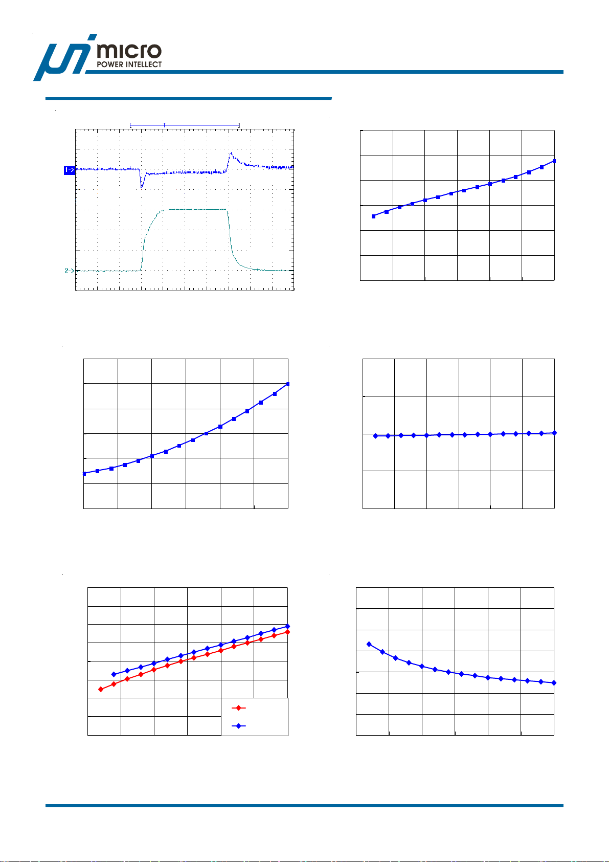
Typical Operation Characteristics
30
25
20
Load Transient Response
V
OUT
(5mV/D iv)
I
OUT
(1A/Div)
25us/Div
C
= 22uF/X5R
OUT
Shutdown Current vs. Input Voltage
Quiescent Current vs. Input Voltage
1000
900
800
700
600
Quiescent Current (uA)
500
400
2.533.544.555.5
Input Voltage V
CNTL
= VIN (V)
Line Regulation
0.81
(V)
0.805
FB
15
10
Shutdown Current (uA)
5
0
2.5 3 3.5 4 4.5 5 5.5
Input Voltage V
CNTL
= VIN (V)
Enable/Disable Threshold vs Input Voltage
1.4
1.3
1.2
1.1
1
0.9
0.8
Disable
0.7
Enable/Disable Threshold (V)
Enable
0.6
0.8
0.795
Feedback Voltage V
0.79
2.533.544.555.5
Input Voltage V
CNTL
= VIN (V)
On Resistance vs. Input Voltage
140
130
120
110
100
90
On Resistance (mΩ)
80
70
2.5 3 3.5 4 4.5 5 5.5
Input Voltage V
uPI Semiconductor Corp., http://www.upi-semi.com
Rev. 00, 2007, April
CNTL
= VIN (V)
2.5 3 3.5 4 4.5 5 5.5
Input Voltage V
CNTL
= 5V, V
OUT
= 0.8V
7
Page 8
uP7701
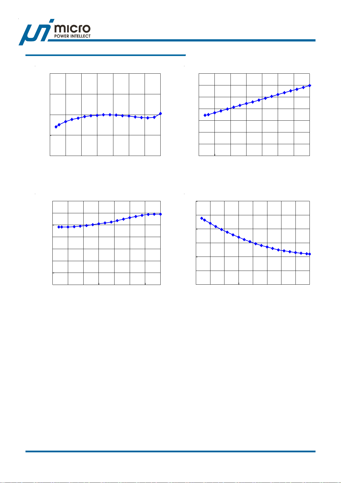
Typical Operation Characteristics
FB Voltage vs. Temperature
810
805
(mV)
FB
800
795
Feedback Voltage V
790
-50-25 0 25 50 75100125
Junction Temperature (OC)
V
= 5V, VIN = V
CNTL
OUT
+ 1V
Quiescent Current vs. Temperature
1400
1200
1000
800
600
400
Quiescent Current (uA)
200
On Resistance vs. Temperature
140
120
100
80
60
40
On Resistance (mΩ)
20
0
-50 -25 0 25 50 75 100 125
Junction Temperature (OC)
V
CNTL
= 5V, V
OUT
= 1.6V
EN Source Current vs. Temperature
30
25
20
15
10
5
EN Pin Source Current (uA)
0
-50 -25 0 25 50 75 100 125
Junction Temperature (OC)
V
= VIN = 5V
CNTL
0
-50 -25 0 25 50 75 100 125 150
Junction Temperature (OC)
V
= 5V
CNTL
uPI Semiconductor Corp., http://www.upi-semi.com
Rev. 00, 2007, April
8
Page 9
uP7701
A
pplication Information
The uP7701 is a high performance linear regulator
specifically designed to deliver up to 3A output current with
very low input voltage and ultra low dropout voltage. With
dual-supply configuration, the uP7701 operates with a wide
input voltage VIN range from 1.0V to 5.5V and is ideal for
applications where VOUT is very close to VIN .
Supply Voltage for Control Circuit V
CNTL
Unlike other linear regulators that use a P-Channel
MOSFET as the pass transistor, the uP7701 uses an NChannel as the pass transistor. N-Channel MOSFET
provides lower on-resistance and better stability meeting
stringent requirements of current generation
microprocessors and other sensitive electronic devices.
The drain of N-Channel MOSFET is connected to VIN and
the source is connected to VOUT. This requires that the
supply voltage V
for control circuit is at least 1.5V higher
CNTL
than the output voltage to provide enough overdrive capability
for the pass transistor thus to achieve low dropout and fast
transient response. It is highly recommended to bias the
device with 5V voltage source if available.
Use a minimum 0.1uF ceramic capacitor plus a 10Ω
resistor to locally bypass the control voltage.
bulk capacitance on the rail. Additionally, bulk capacitance
may be added closely to the input supply pin of the uP7701
to ensure that VIN does not sag, improving load transient
response.
Output capacitor: A minimum bulk capacitance of 10uF,
along with a 0.1uF ceramic decoupling capacitor is
recommended. Increasing the bulk capacitance will improve
the overall transient response. The use of multiple lower
value ceramic capacitors in parallel to achieve the desired
bulk capacitance will not cause stability issues. Although
designed for use with ceramic output capacitors, the uP7701
is extremely tolerant of output capacitor ESR values and
thus will also work comfortably with tantalum output
capacitors.
Thermal Consideration
The uP7701 integrates internal thermal limiting function to
protect the device from damage during fault conditions.
However, continuously keeping the junction near the thermal
shutdown temperature may remain possibility to affect
device reliability. It is highly recommended to keep the
junction temperature below the recommended operation
condition 125OC for maximum reliability.
Input/Output Capacitor Selection
The uP7701 has a fast transient response that allows it to
handle large load changes associated with high current
applications. Proper selection of the of the output capacitor
and it’s ESR value determines stable operation and
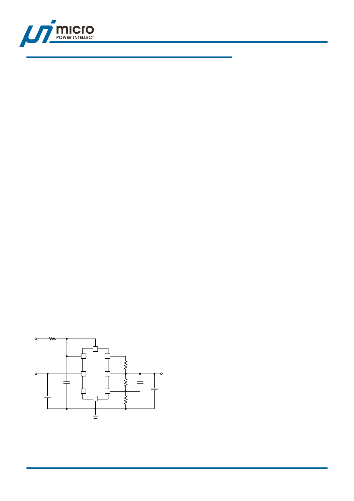
optimizes performance. The typical application circuit
shown in Figure 1 was tested with a wide range of different
capacitors. The circuit was found to be unconditionally
stable with capacitor values from 10uF to 2200uF and ESR
ranging from 0.5mΩ to greater then 75mΩ.
5VCC
R4
10R
V
IN
C1
1uF
C2
4.7uF
EN
NC
CNTL
2
3
5
4
POK
1
R3
10K
VOUTVIN
6
uP7701
7
8
GND
R2
12.5K
FB
R1
10K
C4
option
V
OUT
C3
10uF
Figure 1. Typical Application Circuit
Input capacitor: A minimum of 4.7uF ceramic capacitor
is recommended to be placed directly next to the VIN pin.
This allows for the device being some distance from any
Power dissipation in the device is calculated as:
PD = (VIN - V
OUT
) x I
OUT
+ V
CNTL
x I
CNTL
It is adequate to neglect power loss with respective to
control circuit V
CNTL
x I
when considering thermal
CNTL
management in uP7701 Take the following moderate
operation condition as an example: VIN = 2.5V, V
I
= 2A, the power dissipation is:
OUT
= 1.5V,
OUT
PD = (1.8V- 1.2V) x 2A = 2.0W
This power dissipation is conducted through the package
into the ambient environment, and, in the process, the
temperature of the die (TJ) rises above ambient. Large power
dissipation may cause considerable temperature raise in
the regulator in large dropout applications. The geometry
of the package and of the printed circuit board (PCB) greatly
influence how quickly the heat is transferred to the PCB
and away from the chip. The most commonly used thermal
metrics for IC packages are thermal resistance from the
chip junction to the ambient air surrounding the package
(θ
):
JA
θ
= ( TJ -TA ) / P
JA
θ
specified in the Thermal Information section is measured
JA
D
in the natural convection at TA = 25OC on a high effective
thermal conductivity test board (4 Layers, 2S2P) of JEDEC
51-7 thermal measurement standard. The case point of
θ
is on the exposed pad for PSOP-8 package.
JC
uPI Semiconductor Corp., http://www.upi-semi.com
Rev. 00, 2007, April
9
Page 10
Given power dissipation PD, ambient temperature and
A
thermal resistance θ
, the junction temperature is
JA
calculated as:
TJ = T
+ ∆T
A
= TA + P
JA
D
x θ
JA
To limit the junction temperature within its maximum rating,
the allowable maximum power dissipation is calculated
as:
P
= ( T
D(MAX)
where T
-T
J(MAX)
J(MAX)
) /θ
A
JA
is the maximum operation junction
temperature 125OC, TA is the ambient temperature and the
θJA is the junction to ambient thermal resistance. θ
of
JA
PSOP-8 packages is 75OC/W on JEDEC 51-7 (4 layers,
2S2P) thermal test board with minimum copper area. The
maximum power dissipation at TA = 25OC can be calculated
as:
P
= (125OC - 25OC) / 75OC/W = 1.33W
D(MAX)
The thermal resistance θ
highly depends on the PCB
JA
design. Copper plane under the exposed pad is an effective
heatsink and is useful for improving thermal conductivity.
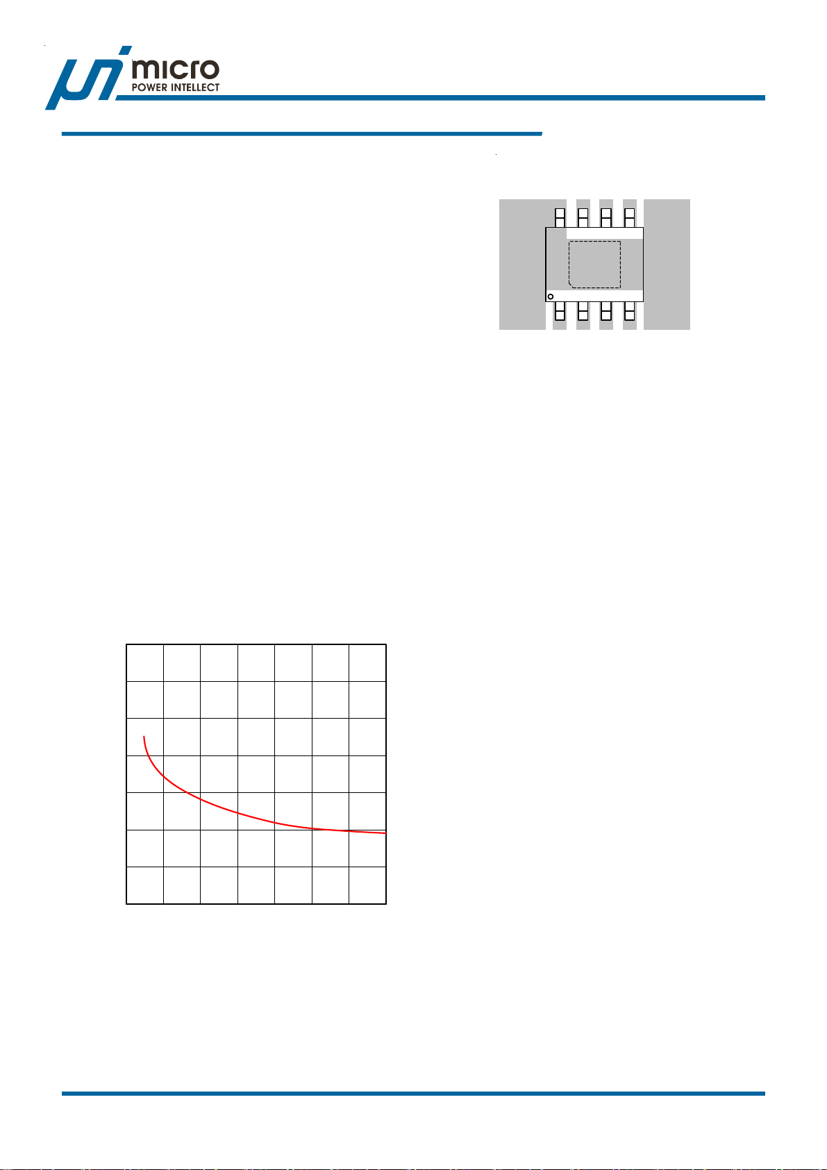
Figure 3 show the relationship between thermal resistance
θ
vs. copper area on a standard JEDEC 51-7 (4 layers,
JA
2S2P) thermal test board at TA = 25OC. A 50mm2 copper
plane reduces θ
from 75OC/W to 52OC/W and increases
JA
maximum power dissipation from 1.33W to 1.9W.
uP7701
pplication Information
FB
VOUT
GNDPOK
7
8
1
2
EN
Figure 4. Recommended PCB Layout.
Layout Consideration
1. Place a local bypass capacitor as closed as possible
to the VIN pin. Use short and wide traces to minimize
parasitic resistance and inductance.
2. The exposed pad should be soldered on GND plane
with maximum area and with multiple vias to inner layer
of ground place for improving thermal performance.
3. Connect voltage divider directly to the point where
regulation is required. Place voltage divider close to
the device.
NC
6
GND
3
uP7701
45
VIN
CNTL
100
90
C/W)
80
O
(
JA
70
60
50
T herm al Re si st a nc e θ
40
30
60 7050403020100
Copper Area (mm2)
Figure 3. Thermal Resistance θ
vs. Copper Area
JA
Figure 4 illustrated the recommended PCB layout for best
thermal performance.
uPI Semiconductor Corp., http://www.upi-semi.com
Rev. 00, 2007, April
10
Page 11
uP7701
A
pplication Information
0.76 REF
1.27 REF
4.80 - 5.00
1.85 REF
2.39 REF
5.80 - 6.20
6.15 REF
8.00 MIN
2.39 REF
4.00 MIN
3.80 - 4.00
2.29 BSC
2.29 BS C
1.27 BSC
0.32 - 0.52
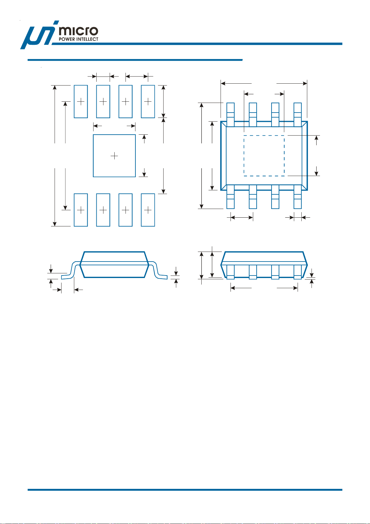
Recommended Solder Pad Layout
1.45 - 1.60
0.20 BSC
0.41 - 0.89
0.18 - 0.25
1.75 MAX
0.10 - 0.25
3.81 BSC
Note
1.Package Outline Unit Description:
BSC: Basic. Represents theoretical exact dimension or dimension target
MIN: Minimum dimension specified.
MAX: Maximum dimension specified.
REF: Reference. Represents dimension for reference use only. This value is not a device specification.
TYP. Typical. Provided as a general value. This value is not a device specification.
2.Dimensions in Millimeters.
3.Drawing not to scale.
4.These dimensions no not include mold flash or protrusions. Mold flash or protrusions shell not exceed 0.15mm.
uPI Semiconductor Corp., http://www.upi-semi.com
Rev. 00, 2007, April
11
 Loading...