

Page 1
Preliminary
A
uP6207
3 Phase Synchronous-Rectif ied Buck Contronller
for Next Genenration CPU Core Power
General Description
The uP6207 is a multi-phase synchronous-re ctif ied buck
controller specifically designed to deliver high quality output
voltage for high-performa nce microprocessors and gra phic
processors. The uP6207 integrates a 5V LDO regulator
that enables it to work with a single 12V supply voltage. It
also integrates bootstrapped drivers that support 12V +
12V driving ca pability .
The uP6207 provides progra mmable 2/3-pha se operation.
It also supports dynamic phase selection by PS1/2 pins
that automatically switches to single/two pha se operation
at light load condition. The uP6207 supports both sta ndalone and tra cking mode operation. The output voltage is
tightly regulated to local or external reference voltages.
The uP6207 extract pha se current signals by R
DS(ON)
of low
side switches for pha se current balance. It sen ses the output
current by DCR of output inductors f or load line slope setting
and over current protection. This yields both thermal balance
and a ccurate load line a djustment.
The uP6207 includes programmable no-load offset and
droop slope functions to adjust the output voltage as a
function of the load current, optimally positioning it for a
system transient.
Other features include a ccurate and relia ble short-circuit
protection, adjustable over current protection, a nd a delayed
power OK output. This part is available in VQF N5x5 - 32L
package.
pplications
Features
Interleaved Two/Three Phase Operation
Programmable Dynamic Power Saving Mode
Operation
Simple Single-Loop Voltage-Mode Control
Integrated 12V Bootstrapped Drivers with
Internal Bootstra p Diode
Lossless R
Current Sensing for Current
DS(ON)
Balance
Adjustable Operation Frequency form 50kHz to
1MHz Per Phase
External Compensation
Adjustable Over Current Protection
Adjustable Soft Start
VQFN5x5 -32L Package
RoHS Compliant and 100% Lead (Pb)-Free
Ordering Inf o rmation
rebmuNredrOepyTegakcaPkrameR
IAQA7026PuL23-5x5NFQV
Note: uPI products are compatible with the current IPC/
JEDEC J-STD-020 a nd RoHS requirements. They are 100%
matte tin (Sn) plating and suitable f or use in SnPb or Pbfree soldering processes.
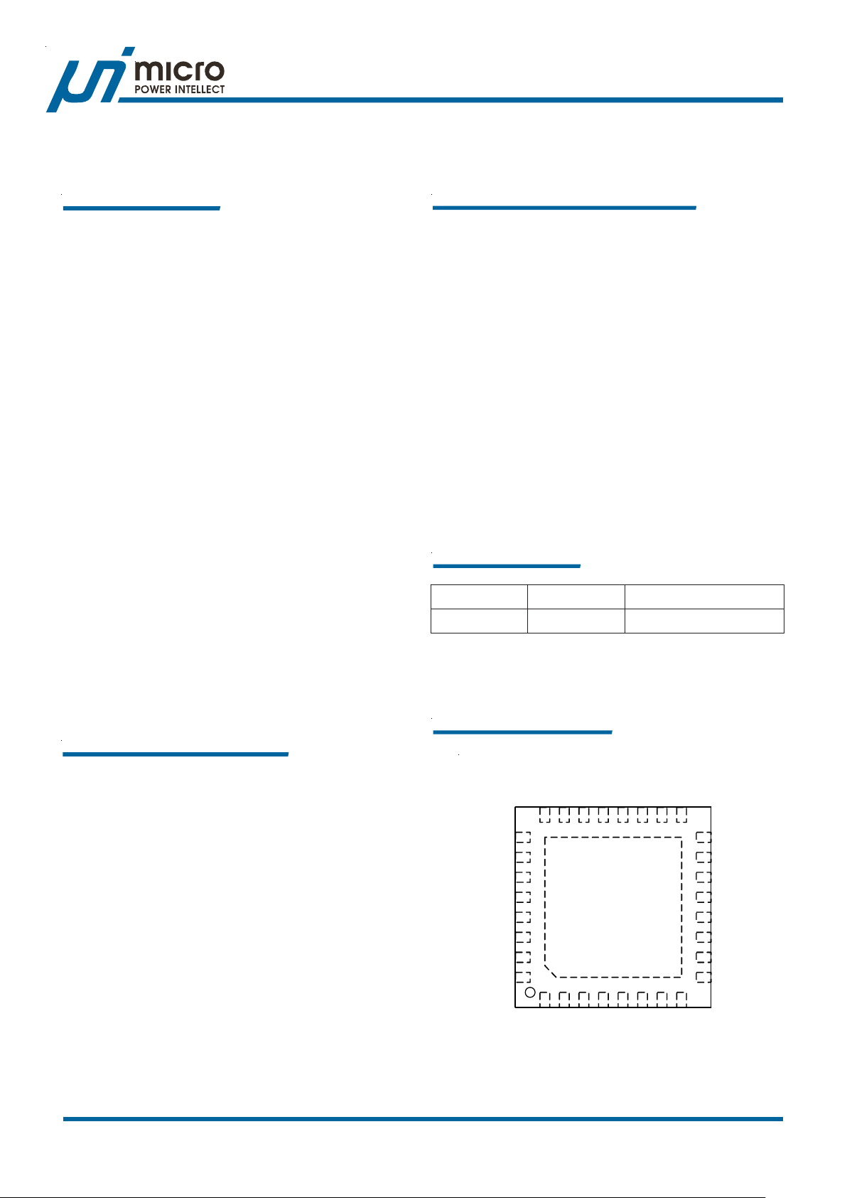
Pin Configuration
Desktop PC Core Power Supplies
Middle/High End Graphic Cards
Low Output Voltage, High Power Density DC/DC
Converters
Voltage Regulator Modules
uPI Semiconductor Corp., http://www.upi-semi.com
Rev. P00, File Name: uP6207-DS-P0000
LG3
VCC12B
LG2
PH2
UG2
BOOT2
VCC12A
PH3
UG3
23 22 2124
25
26
27
28
29
30
31
32
PH1
UG1
RT
VCC5
EN
20 19
REFIN
65
ISNE1
FBRTN
ISNE2
SS
1718
87
ISEN3
POK
16
15
14
13
12
11
10
9
PS1
OFS
IMAX
CSN
CSP
COMP
FB
PS2LG1
1
BOOT3
GND
4321
BOOT1
Page 2
Preliminary
VCC12A
BOOT1
uP6207
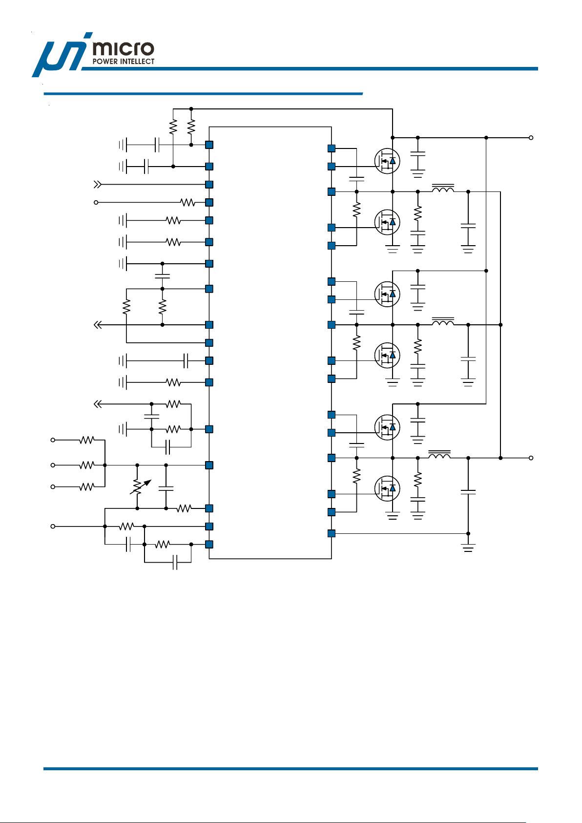
T ypical Applic ation Circui t
V
IN
PH3
PH1
PH2
V
OUT
VCC12B
EN
V
REF
REFIN
PS1
PS2
GND
VCC5
POK
OFS
SS
RT
IMAX
CSP
CSN
FB
COMP
UG1
PH1
LG1
ISEN1
BOOT2
UG2
PH2
LG2
ISEN2
BOOT3
UG3
PH3
LG3
ISEN3
FBRTN
V
OUT
uPI Semiconductor Corp., http://www.upi-semi.com
Rev. P0000, File Name: uP6207-DS-P0000
2
Page 3

.oNemaNnoitcnuFniP
n
Preliminary
uP6207
Function al Pin Descripti o
11HP
21GU
31TOOB
4NE
5NIFER
6NTRBF
7SS
8KOP
92SP
01BF
11PMOC
21PSC
31NSC
.1esahProfniPesahP atcennoC.1esahprofrevirdetagreppufohtapnruterehtsinipsihT
ehtforevirdetagreppuroftiucricpartstoobamrofot1TOOBotnipsihtmorfroticapac
.1esahProfrevirDetaGreppU
.1esahProfTOOB reppuroftiucricpartstoobamrofot1HPotnipsihtmorfroticapacatcennoC
.1esahpehtforevirdetag
.elbanEpihC ecivedehtnwodstuhsV4.0nahtrewolnipsihtgnilluP .
.tupnIecnerefeRlanretxE .rotsiserahguorhtegatlovecnereferlanretxenaotnipsihttcennoC
aolehtstesrotsiserehT
.detaluger
.tratStfoS .emittratstfosehttesotDNGotnipsihtmorfroticapacatcennoC
ewoP
uder
.niPkcabdeeF .reifilpmarorreehtfotupnignitrevniehtsinipsihT
.noitacidnIdooGr
.leveldlohserhtnoitc
.tuptuOnoitasnepmoC reifilpmaror
uCehtfotupnIevitageN
.epolsenild
ennoC
.tiucriCecnerefeRehtrofnruteR ebotsiegatlovtuptuoerehwtniopdnuorgehtotsihttc
.2tupnIgnitteSedoMgnivaSrewoP esahpehttesotDNGotnipsihtmorfrotsiseratcennoC
reehtfotuptuoehtsinipsihT
.reifilpmAMGgnisneStnerruCehtfotupnIevitisoP
.reifilpmAMGgnisneStnerr
.TEFSOMreppu1esahpfoetagehtnipsihttcennoC
.1esahp
41XAMI
51SFO
611SP
.noitacidnItnerruCtuptuO tnerrucrevoehttesotDNGotnipsihtmorfrotsiseratcennoC
.
levelnoitcetorp
.tesffOtnerruCoreZ tesffotuptuoehttesotDNGro5CCVotnipsihtmrofrotsiseratcennoC
.egatlov
.1tupnIgnitteSedoMgnivaSrewoP esahpehttesotdnuorgotnipsihtmorfrotsiseratcennoC
.leveldlohserhtnoitcuder
uPI Semiconductor Corp., http://www.upi-semi.com
Rev. P00, File Name: uP6207-DS-P0000
3
Page 4

n
.oNemaNnoitcnuFniP
Preliminary
uP6207
Function al Pin Descripti o
713NESI
812NESI
911NESI
02TR
125CC
V
223TOOB
323GU
423HP
523GL
62B21CCV
722GL
822HP
922GU
.3esahProfgnisneStnerruC
.2esahProfgnisneStnerruC
erruC
.ycneuqerf
.tuptuOODLV5 .ODLV5lanretniehtfoniptuptuoehtsinipsihT
.3esahProfTOOB reppuroftiucricpartstoobamro
virDetaGrewoL .TEFSOMrewol3esahpfoetagehtotnipsihttcennoC
.tupnIylppuS .stiucriclortnocdnasrevird
.1esahProfgnisneStn
.3esahpehtforevirdetag
.3esahProfniPesahP atcennoC.3esahprofrevirdetagreppufohtapnruterehtsini
.2esahProfniPesahP atcennoC.2esahprofrevirdetagreppufohtapnruterehtsinipsihT
.gnimmargorPycneuqerFgnihctiwS gnihctiwsehttesotDNGotnipsihtmorfrotsiseratcennoC
fot3HPotnipsihtmorfroticapacatcennoC
.3esahProfrevirDetaGreppU .TEFSOMreppu3e
psihT
.3esahProfre
etagroftnerrucseilppusnipsihT
.2esahProfrevirDetaGrewoL .TEFSOMrewol2esahpfoetagehtotnipsihttcennoC
.2esahProfrevirDetaGreppU .TEFSOMreppu2e
sahpfoetagehtnipsihttcennoC
.3esahpehtforevirdetagreppuroftiucricpartstoobamrofot3TOOBotnipsihtmorfroticapac
reppuroftiucricpartstoobamrofot2TOOBotnipsihtmorfroticapac
sahpfoetagehtnipsihttcennoC
.2esahpehtforevirdetag
032TOOB
13A21CCV
231GL
.2esahProfTOOB reppuroftiucricpartstoobamrofot2HPotnipsihtmorfroticap
.2esahpehtforevirdetag
.tupnIylppuS .stiucriclortnocdnasrevirdetagroftnerrucseilppusni
psihT
daPdesopxE
oP iT noitcennocecnadepmitsewolehthguorhtenalp/dnalsidnuorgehtotnipsihte
DNGP
.elbaliava
.dnuorGrew
acatcennoC
.1esahProfrevirDetaGrewoL .TEFSOMrewol1esahpfoetagehtotnipsihttcennoC
uPI Semiconductor Corp., http://www.upi-semi.com
Rev. P0000, File Name: uP6207-DS-P0000
4
Page 5
GND
RT
PS1
PS2
CSP
1.2V
Oscillator
CSN
Preliminary
uP6207
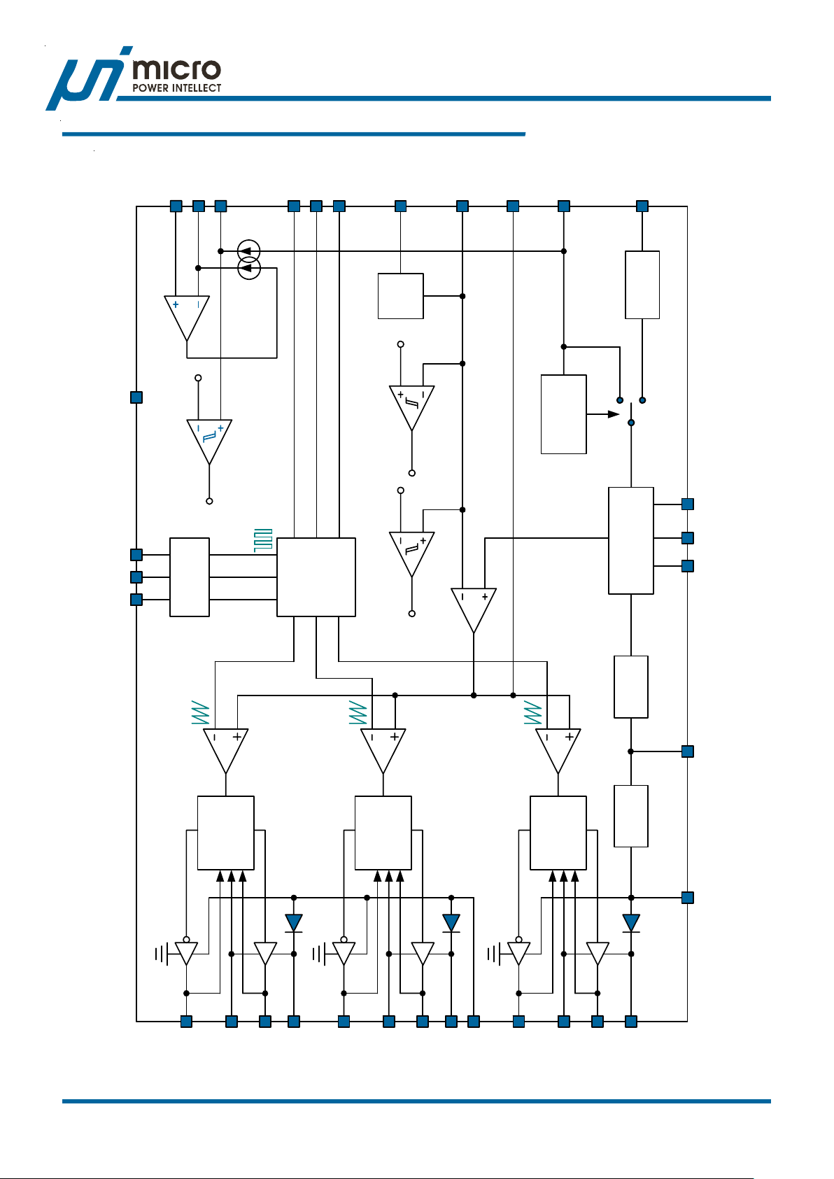
Functional Block Diagram
IMAX
OCP
ISEN3
Balance
OFS Offset
300mV
V
EAP
–
UVP OVP
160mV
V
EAP
+
Current
FB
ISEN1
ISEN2
COMP
REFIN
Band GapFBRTN
V
REFIN
0.8V V
REF
Reference
Selection
Power OK
Soft Start
V
EAP
&
POK
EN
SS
LG3
POR
PWM3
Control
Logic
Gate
BOOT3
UG3
PH3
LG2
PWM2
Control
Logic
Gate
BOOT2
UG2
PH2
LG1
VCC12B
PWM1
VCC5
Control
Logic
Gate
PH1
LDO
BOOT1
UG1
VCC5
VCC12A
uPI Semiconductor Corp., http://www.upi-semi.com
Rev. P00, File Name: uP6207-DS-P0000
5
Page 6
Preliminary
uP6207
Functional Descri ption
The uP6207 is a multi-phase synchronous-re ctified buck
controller specifically designed to deliver high quality output
voltage for high-performa nce micro processors and gra phic
processors. The uP6207 integrates a 5V LDO regulator
that enables it to work with a single 12V supply voltage. It
also integrates bootstrapped drivers that support 12V +
12V driving ca pability .
The uP6207 provides progra mmable 2/3-pha se operation.
It also supports dynamic phase selection by PS1/2 pins
that automatically switches to single phase operation at
light load condition. The uP6207 supports both sta nd-alone
and tra cking mode operation. The output voltage is tightly
regulated to local or external reference voltages.
The uP6207 extract pha se current signals by R
DS(ON)
of low
side switches for pha se current balance. It sen ses the output
current by DCR of output inductors f or load line slope setting
and over current protection. This yields both thermal balance
and a ccurate load line a djustment.
The uP6207 includes programmable no-load offset and
slope functions to adjust the output voltage as a function
of the load current, optimally positioning it for a system
transient.
Other features include accurate and relia ble short-circuit
protection, adjustable over current protection, a nd a delayed
power OK output. This part is available in VQF N5x5 - 32L
package.
Supply Input and Power on Reset
The uP6207 receives supply input from VCC12A/B pins to
provide current to gate drivers. RC filters are required for
locally bypassing the supply input pins. Since only the
VCC12A pin is monitored for power on reset, make sure
the VCC12A/B pins are connected to the sa me voltage
source externally.
Reference Voltage Selection
The uP6207 supports both stand alone a nd tra cking mode
operation. REFIN voltage is checked at VCC5 POR for
reference voltage selection a s shown in Figure 1. The FB
voltage is regulated to internal 0.8V reference voltage if V
REFIN
is higher than 4V at VCC POR. Otherwise, the FB voltage
is regulated to track V
. See the Voltage Control Loop
REFIN
section for details.
SS
0.4V
0.8V V
4.0V
REF
uP6207
V
EAP
FBRTN
REFIN
Band
Gap
V
REFIN
Figure 1. Reference V oltage Selection.
Oscillation Frequency Programming
A resistor RRT connected to RT pin progra ms the oscillation
frequency a s:
=
10000
RT
)k(R
Ω
(kHz)
f
OSC
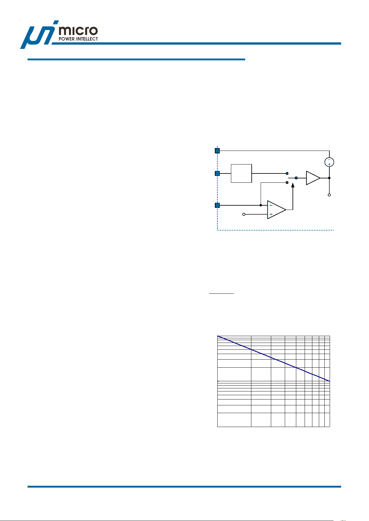
Figure 2 shows the relationship between oscillation
frequency and RRT.
1000
An internal 5V LDO regulator provides a regulated 5V
voltage source to power the internal control circuit. Pla ce
a minimum 1uF cera mic ca pacitor physically near the VCC5
pin for locally bypassing the VCC5 voltage. The VCC5
voltage is continuously monitored for power on reset. The
POR level is typical 4.2V at VCC5 rising.
Operation Phase Selection
The uP6207 supports 2/3 phase operation. PS2 status is
checked at POR for operation phase selection. 2 phase
operation is selected if PS2 < 0.1V at VCC5 POR. When
operating at 2 phase, pha se 3 is turned of f and clock signals
of pha se1/2 are kept output of pha se. When operating at 3
phase, clock signals are kept 120OC difference to each
other. Leave gate drivers a nd ISEN3 floating when operating
in 2 phase.
uPI Semiconductor Corp., http://www.upi-semi.com
Rev. P0000, File Name: uP6207-DS-P0000
100
Switching Frequency (kHz)
10
10 100
R
(kohm)
RT
Figure 3. Switching Frequency vs. RRT.
6
Page 7
Preliminary
uP6207
Functional Descri ption
Output Current Sensing
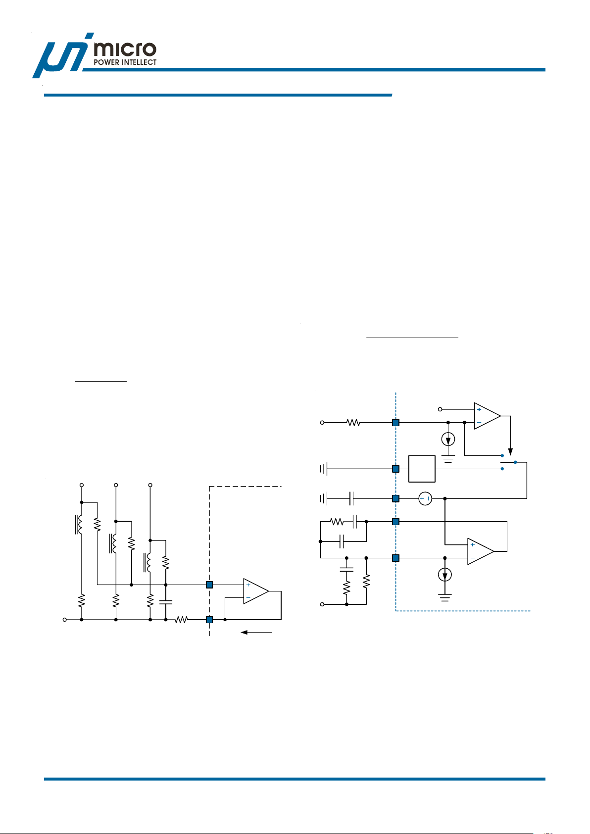
Figure 3 illustrates the output current sensing block of the
uP6207. The voltage VCS across the current sensing
ca pa citor CCS can be expressed as:
= I
VCS
x DCR/P
OUT
if the following condition is true.
P x L / DCR = R
CSP
x C
CS
where P is the phase number of operation (P = 2 for two
pha se operation, P = 3 for three phase operation), L is the
output inductor of the buck converter, DCR is the para sitic
resistance of the inductor , R
and CCS are the external RC
CSP
network for current sensing.
The GM a mplifier will source a current I
to the CSN pin to
AVG
let its inputs virtually short circuit.
I
x R
AVG
Therefore the output current signal I
CSN
= V
CS
can be expressed
AVG
as:
DCRI
×
I
AVG
The output current signal I
OUT
=
RP
×
CSN
is used a s droop tuning a nd
AVG
output over current protection. Please see the related
section for details.
PH1
PH2
R
CSP
PH3
V
= V
EAP
where V
- K x R
EXT
is a slew rate limited voltage source, I
EXT
DROOP
x I
AVG
AVG
is a
current source proportional to output current, K a current
mirror gain (K = 3 for three pha se operation, K = 2 f or two
phase operation) and R
is an external resistor for
DROOP
adjusting load line slope.
The FB pin voltage VFB is expressed a s:
VFB = V
where V
- RFB x I
OUT
is the output voltage, I
OUT
OFS
is a current source
OFS
for initial of fset adjustment, RFB is an external resistor.
The Error Amplifier modulates the COMP voltage V
COMP
and
the duty cycle of buck converter to force FB voltage V
follows V
V
= V
OUT
OUT
. Therefore, the output voltage will be:
EAP
- K x R
EXT
VV ×+
−=
EXT
DROOP
x I
R
AVG
××
CSN
+ RFB x I
RDCRI
DROOPOUT
OFS
IR
OFSFB
Plea se see the related section f or details.
4.0
SS
V
REFIN
Band
K x I
Gap
0.4V
AVG
0.8V V
V
EAP
REF
V
EXT
R
DROOP
FBRTN
C
SS
REFIN
COMP
FB
R
L
L
V
OUT
CSP
uP6207
R
CSP
L
DCRDCRDCR
CSP
C
CS
CSN
R
CSN
GM
Amplifer
I
AVG
Figure 3. Output Current Sensing of uP6207.
Voltage Control Loop (External Reference Voltage)
Figure 4 illustrates the voltage control loop for external
reference voltage of the uP6207. VFB and V
are negative
EAP
and positive inputs of the Error Amplifier re spectively . The
EAP pin voltage is expressed a s:
uPI Semiconductor Corp., http://www.upi-semi.com
Rev. P00, File Name: uP6207-DS-P0000
FB
I
R
V
OUT
FB
OFS
Error
Amplifier
uP6207
Figure 4. V oltage Control Loop for External Reference.
Plea se note the external reference voltage V
changing
EXT
slew rate should be limited to a safe level. A large step
change of V
should be avoid a s it may re sult in large
EXT
inrush current to charge and discharge the output
capacitors and result in false triggering of OCP, UVP
and OVP protection functions.
Voltage Control Loop (Internal Reference Voltage)
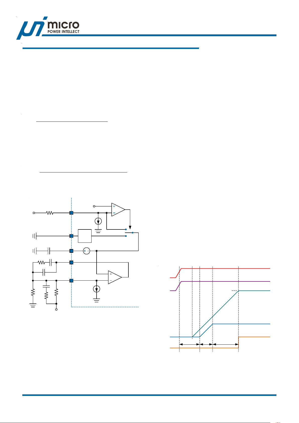
Figure 5 illustrates the voltage control loop for internal
7
Page 8
Preliminary
uP6207
Functional Descri ption
reference voltage of the uP6207. VFB and V
are negative
EAP
and positive inputs of the Error Amplifier re spectively . The
Error Amplifier modulate s the COMP voltage V
COMP
and the
duty cycle of buck converter to force FB voltage VFB follows
V
.
EAP
V
= 0.8V
EAP
Note that there is no droop function when internal reference
voltage is selected.
RRIVR
××−×
V
=
FB
where V
is the output voltage, I
OUT
RR
+
for initial off set adjustment, R
2FB1FB
FB1
and R
2RFB1FBOFSOUT2FB
is a current source
OFS
are external resistor
FB2
divider for voltage setting.
Therefore, the output voltage will be:
RRI)RR(V8.0
××++×
V
OUT
=
R
2FB
2FB1FBOFS2FB1FB
Plea se see the related section f or details.
4.0V
SS
V
REFIN
Band
K x I
Gap
0.4V
AVG
0.8V V
V
EAP
REF
VCC5
R
DROOP
FBRTN
C
SS
REFIN
COMP
The offset current source I
is mirrored and inje cted to FB
OFS
pin for initial offset adjustment. Please see the Voltage
Control Loop section for details.
Soft Start and Power OK
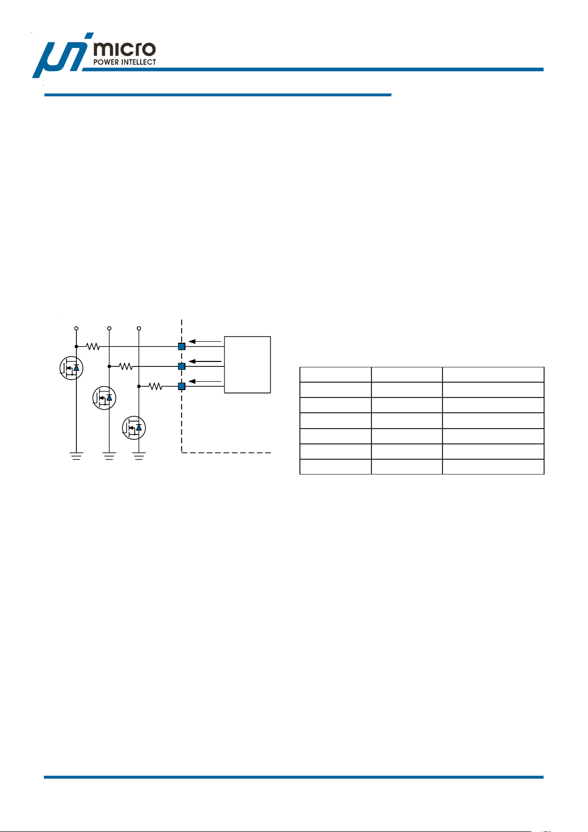
Figure 6 illustrates the soft start cycle of uP6207. A ca pacitor
CSS connected to SS pin is used to adjust the soft start
cycle.
A 10uA current source ISS is used to charge/discharge C
during soft start and V
to 0.4V higher tha n V
V
during soft start and V
EAP
changes. Since Vss is cla mped
REFIN
, this limit the slew rate of VSS and
EAP
changes. This con sequently
REFIN
limits the output voltage ra mp up/down slew rate.
The uP6207 is POR and ena bled at T0. There is a 800us
time delay (T0 ~ T1) before the current source ISS begins
charging the CSS. The non-inverting input V
voltage V
is kept zero during (T0 ~ T2). The V
OUT
and output
EAP
EAP
and
VOUT ra mps up to target value during ti me delay T D2. The
uP6207 inserts a time delay T D3 before a ssertion of power
OK. The uP6207 asserts soft start end and set POK to
high impeda nce status at T4.
Time periods are calculated a s:
(T2 - T1) = 0.4V x CSS / 10uA
T D1 = T2 - T0 = 800us + 0.4V x CSS / 10uA
TD2 = V
T D3 = (4.1V - V
where V
0.8V for internal reference voltage, V
x CSS / 10uA = V
BOOT
) / 10uA
EAP
is the initial boot up reference voltage. V
BOOT
x CSS / 10uA
EAP
BOOT
= V
for external
EXT
BOOT
reference voltage.
SS
=
FB
I
R
FB2
R
FB1
V
OUT
OFS
uP6207
Error
Amplifier
Figure 5. V oltage Control Loop for Internal Reference.
Initial Offset Adjustment
Connect a resistor R
set the initial offset voltage. The OFS voltage V
from OFS pin to VCC5 or GND to
OFS
OFS
is V
CC5
1.6V or 0.4V when connected to VCC5 or GND respectively.
There the current source I
I
= 0.4V / R
OFS
I
= 1.6V / R
OFS
uPI Semiconductor Corp., http://www.upi-semi.com
Rev. P0000, File Name: uP6207-DS-P0000
sourcing, R
OFS
sinking, R
OFS
can be calculated a s:
OFS
to GND, positive of fset
OFS
to VCC5, negative offset.
OFS
VCC5
EN
V
OUT
-
VR_RDY
T0 T1 T2 T3
TD2TD1
V
4.5V
SS
TD3
T4
Figure 6. Soft Start Cycle of the uP6207.
8
Page 9
Preliminary
uP6207
Functional Descri ption
Channel Current Sensing
The uP6207 extracts phase currents for current balance
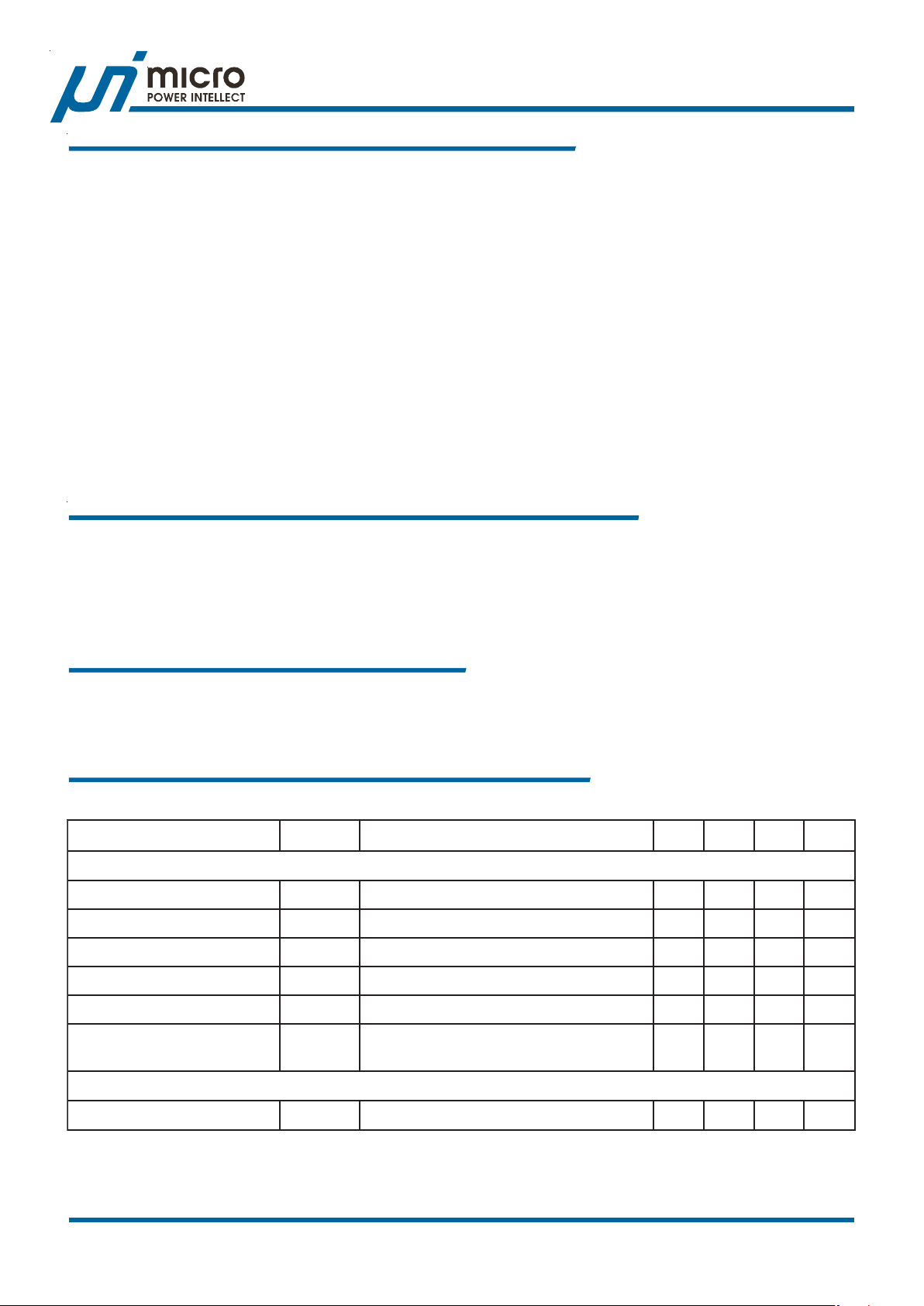
and over current protection by para sitic on-resista nce of the
lower switches when turn on as shown in Figure 7. The
ISEN1/2/3 pins sense the corresponding pha se current when
the low side MOSFETs are turns on.
I
= ((I
SENX
where I
I
is phase current, R
PHX
x R
PHX
is the sampled and held phase current signal,
SENX
DS(ON)
) + VDC) / R
DS(ON)
SENX
is the on-resistance of the low
side MOSFET s, a nd VDC is an off set voltage for the current
balance circuit. The current balance circuit increases the
duty cycle of the phase whose phase current is smaller
than others a nd decrease the duty cycle of the pha se whose
phase current is larger tha n others.
PH2PH1 PH3
I
I
I
SEN1
SEN2
SEN3
Current
Balance
ISEN1
R
SEN1
R
SEN2
R
SEN2
ISEN2
ISEN3
uP6207
Figure 7. Pha se Current Sensing and Current Bala nce.
Select R
is to keep I
to set the current balance gain. A rule of thumb
SEN
= 5uA at rated output current.
SENX
Output Over Current Protection
I
is mirrored and injected to the IMAX pin and create a
AVG
voltage V
V
= K x R
IMAX
at IMAX pin.
IMAX
x I
IMAX
AVG
= R
IMAX
x I
x DCR / R
OUT
CSN
The over current protection is activated a nd shuts down the
uP6207 if the IMAX voltage is higher than 1.2V .
Output Over V oltage Protection
The OVP is a ctivated and turns on the low side MOSFETs
if ( VFB - V
) > 160mV
EAP
The over voltage protection is latch-off a nd can only be reset
by POR or toggling the EN pin.
Under Voltage Protection
The uP6207 sources a 10uA current source out of PS1 a nd
PS2 pins. Connecting resistors R
PS2 pins creates voltage levels V
PS1
PS1
and R
and V
at PS1 and
PS2
for power
PS2
saving mode operation.
V
= 10uA x R
PS1
V
= 10uA x R
PS1
PS1
PS1
T able 1 shows the operation pha se of uP6207 a ccording to
V
, V
, V
IMAX
PS1
. Ta ke V
PS2
= 0.2V, V
PS1
= 0.3V and V
PS2
IMAX
=
0.25V for example, the uP6207 turns off phase 3 and
operates the converter in 2-pha se. Note that the uP6207 do
not reset the clock sequence during dynamic phase
reduction. Phase 1 a nd phase 2 still ha s 120O pha se shift.
The automatic phase reduction reduce s the switching and
conduction losses at light load condition a nd enables high
efficiency over a wide ra nge of output current.
R
PS2
> R
is recommended when programming the
PS1
phase-reduction thre shold level.
T able 1. Operation Pha se Sele ction.
V
1SP
V
2SP
esahPnoitarepO
V8.0>X 3/2/1
V<
XAMI
V>
XAMI
V<
XAMI
V<
XAMI
V>
XAMI
V1.0<2/1
V1.0<1
V<
XAMI
V>
XAMI
V>
XAMI
3/2/1
2/1
1
The under voltage protection is activated if FB voltage V
is 300mV lower than the V
. UVP turns off and latches
EAP
FB
the uP6207.
Power Saving Mode and Automatic Phase Reduction
uPI Semiconductor Corp., http://www.upi-semi.com
Rev. P00, File Name: uP6207-DS-P0000
9
Page 10
Preliminary
A
g
n
uP6207
bsolute Ma x imum Ratin
Supply Input Voltage, VCC12 (Note 1) --------------------------------------------------------------------------------------------- -0.3V to +15V
PHx to GND
DC ------------------------------------------------------------------------------------------------------------------------------------------ -1V to 15V
< 200ns ---------------------------------------------------------------------------------------------------------------------------------- -5V to 30V
BOOTx to PHx ------------------------------------------------------------------------------------------------------------------------------- -0.3V to +15V
UGx to PHx ------------------------------------------------------------------------------------------------------------ -0.3V to (BOOTx - PHx +0.3V)
LGx ----------------------------------------------------------------------------------------------------------------------------- -0.3V to + (VCC12 + 0.3V)
Other Pins -------------------------------------------------------------------------------------------------------------------------------------- -0.3V to +6V
Storage T emperature Range ------------------------------------------------------------------------------------------------------------- -65OC to +150OC
Junction T emperature ------------------------------------------------------------------------------------------------------------------------------------ 150OC
Lead T emperature (Soldering, 10 se c) ------------------------------------------------------------------------------------------------------------ 260OC
ESD Rating (Note 2)
HBM (Human Body Mode) --------------------------------------------------------------------------------------------------------------------- 2kV
MM (Machine Mode) ----------------------------------------------------------------------------------------------------------------------------- 200V
Thermal Informatio
Package Thermal Resistance (Note 3)
VQF N5x5 - 32L θJA -------------------------------------------------------------------------------------------------------------------------------- TBD
VQF N5x5 - 32L θ
-------------------------------------------------------------------------------------------------------------------------------- TBD
JC
Power Dissipation, PD @ TA = 25°C
VQF N5x5 - 32L ------------------------------------------------------------------------------------------------------------------------------------- TBD
Recommen de d Op er at i o n Conditi on s
Operating Junction T emperature Ra nge (Note 4) ------------------------------------------------------------------------ -40°C to +125°C
Operating Ambient T emperature Range -------------------------------------------------------------------------------------- -40°C to +85°C
Supply Input Voltage, V
CC12A/B
------------------------------------------------------------------------------------ 10.8V to 13.2V
Electrical Characteristics
(VCC12A/B = 12V, VCC5 = 5V, TA = 25OC, unless otherwise specified)
retemaraPlobmySsnoitidnoCtseTniMpyTxaMtinU
tupnIylppuS
egatloVtupnIylppuSV
tnerruCylppuSI
dlohserhTROP21CCVV
siseretsyHROP21CCVV
ycaruccAegatloV5CCVV
tuptuOmumixaM5CCV
tnerruC
21CC
21CC
V
HTR21CC
SYH21CC
5CC
I
5CC
21CC
.gnisiR0.70.80.9V
gnihctiwS;nepOxGLdnaxGU--5--Am
8.01--2.31V
--9.0--V
3.5--7.5V
02----Am
tratStfoS
tnerruCtratStfoSI
uPI Semiconductor Corp., http://www.upi-semi.com
Rev. P0000, File Name: uP6207-DS-P0000
V
SS
V0=90111Au
SS
10
Page 11
Preliminary
uP6207
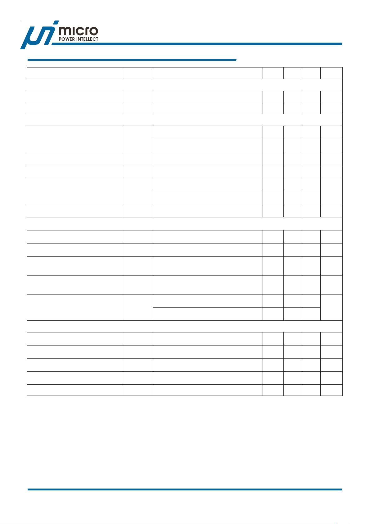
Electrical Characteristics
retemaraPlobmySsnoitidnoCtseTniMpyTxaMtinU
lortnoCelbanE
dlohserhTwoLcigoLV
dlohserhThgiHcigoLV
LI
HI
----4.0V
8.0----V
rotallicsO
R
ycneuqerFgnihctiwSf
CSO
R
k33= Ω noitarepOesahP-3.072003033zHk
TR
k42= Ω noitarepOesahP-3.072003033zHk
TR
egnaRycneuqerFelbatsujdA 05--0001zHk
edutilpmApmaR --4--V
hP-2--78--
yruDmumixaM
noitarepOesa
%
noitarepOesahP-3--09--
egatloVniPTRV
TR
--1--V
CADdnaegatloVecnerefeR
egatloVecnerefeRlanretnI 97.008.018.0V
ycaruccAegatloVtuptuOV
dlohserhTnoitceleSecnerefeR
leveL
V
LI
V-
NIFER
V,
BF
NIFER
.V2.1=01---01Vm
egatloVecnerefeRlanetnItceleS0.4--V
5CC
V
egatloVecnerefeRlanretxE
egnaR
egatloVSFO
V
NIFER
R
R
k01= Ω V.5CCVot
SFO
k01= Ω .DNGot--4.0--
SFO
V-
5CC
SFO
4.0--5.3V
--6.1--
reifilpmArorrE
niaGCDpooLnepOOAngiseDybdeetnarauG0708--Bd
tcudorPhtdiwdnaB-niaGWBGC
DAOL
.Fp5=03----zHM
etaRwelSRSngiseDybdeetnarauG36--su/V
ecnatcudnoc-snarTMGR
)kniS&ecruoS(tnerruCmumixaMI
PMOC
V
k02= Ω 00210061--V/Au
DAOL
V6.1=003063--Au
PMOC
V
uPI Semiconductor Corp., http://www.upi-semi.com
Rev. P00, File Name: uP6207-DS-P0000
11
Page 12
Preliminary
uP6207
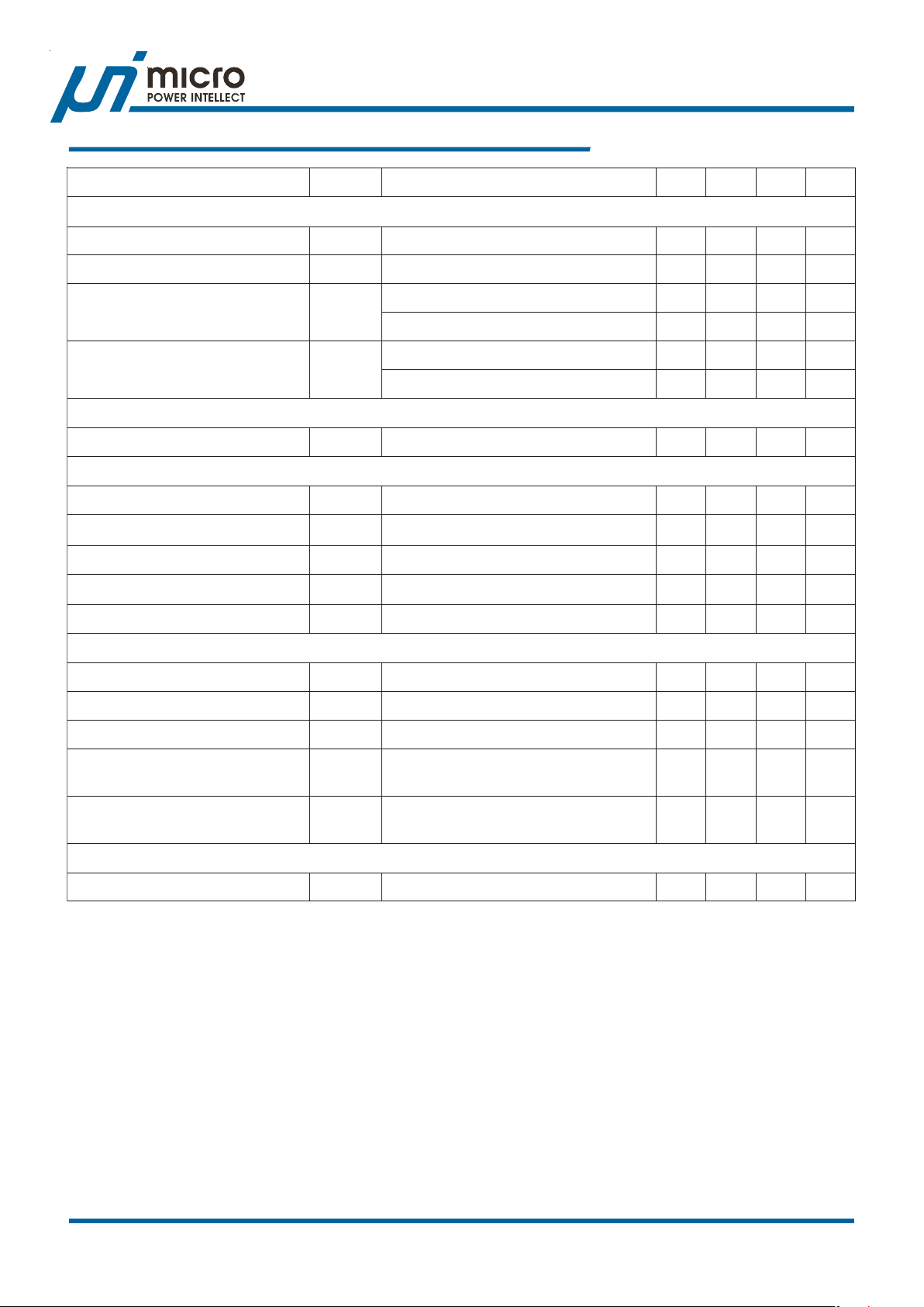
Electrical Characteristics
retemaraPlobmySsnoitidnoCtseTniMpyTxaMtinU
esneStnerruC
tnerruCgnicruoSmumixaM 001----Au
egatloVtesffOtupnI 3---3Vm
I
I/
XAMI
ruccArorriMtnerruCXAMI
yca
ycaruccArorriMtnerruCpoorD
GVA
I/
I
XAMI
GVA
I/
I
POORD
GVA
I/
I
POORD
GVA
edoMgnivaSrewoP
R
tnerruCgnicuoS2SP/1SPI
XSP
R=
1SP
k74= Ω 90111Au
2SP
srevirDetaG
noitarepoesahpeerhtrof--003--%
noitarepoesahpowtrof--002--%
noitarepoesahpeerhtrof--003--%
noitarepoesahpowtrof--002--%
ecruoSetaGreppUI
kniSetaGreppUR
ecruoSetaGrewoLI
kniSetaGrewoLR
emiTdaeDT
V
CRS_GU
V
KNS_GU
VCCV-
CRS_GL
V
KNS_GL
TD
V-
TOOB
V-
ETAGU
V1=--8.06.1 Ω
ETAGL
V6=--2---A
ETAGU
V1=--12Ω
ESAHP
V6=--2---A
ETAGL
--03--sn
noitcetorP
dlohserhTnoitcetorPnerruClatoTV
noitcetorPegatloVrevOBFV
noitcetorPegatloVrednUBFV
XAMI
V-
BF
PAE
V-
BF
PAE
noitcetorPerutarepmeTrevO
dlohserhT
noitcetorPerutarepmeTrevO
siseretsyH
--2.1--V
--061--Vm
--003---Vm
--061--
--02--
O
O
ecneuqeSrewoP
ytilibapaCgnikniSKOPV
I
KOP
KOP
.Am4=--50.02.0V
Note 1. Stresses listed a s the above “Absolute Maximum Ratings” may cause permanent damage to the device.
These are for stress ratings. Functional operation of the device at the se or any other conditions beyond those
indicated in the operational sections of the specifications is not implied. Exposure to absolute maximum
rating conditions for extended periods may remain possibility to af fect device relia bility .
Note 2. Devices are ESD sensitive. Handling pre caution recommended.
Note 3. θJA is mea sured in the natural convection at TA = 25°C on a low effective thermal conductivity test board of
JEDEC 51-3 thermal mea surement standard.
Note 4. The device is not guaranteed to function outside its operating conditions.
C
C
uPI Semiconductor Corp., http://www.upi-semi.com
Rev. P0000, File Name: uP6207-DS-P0000
12
Page 13
Preliminary
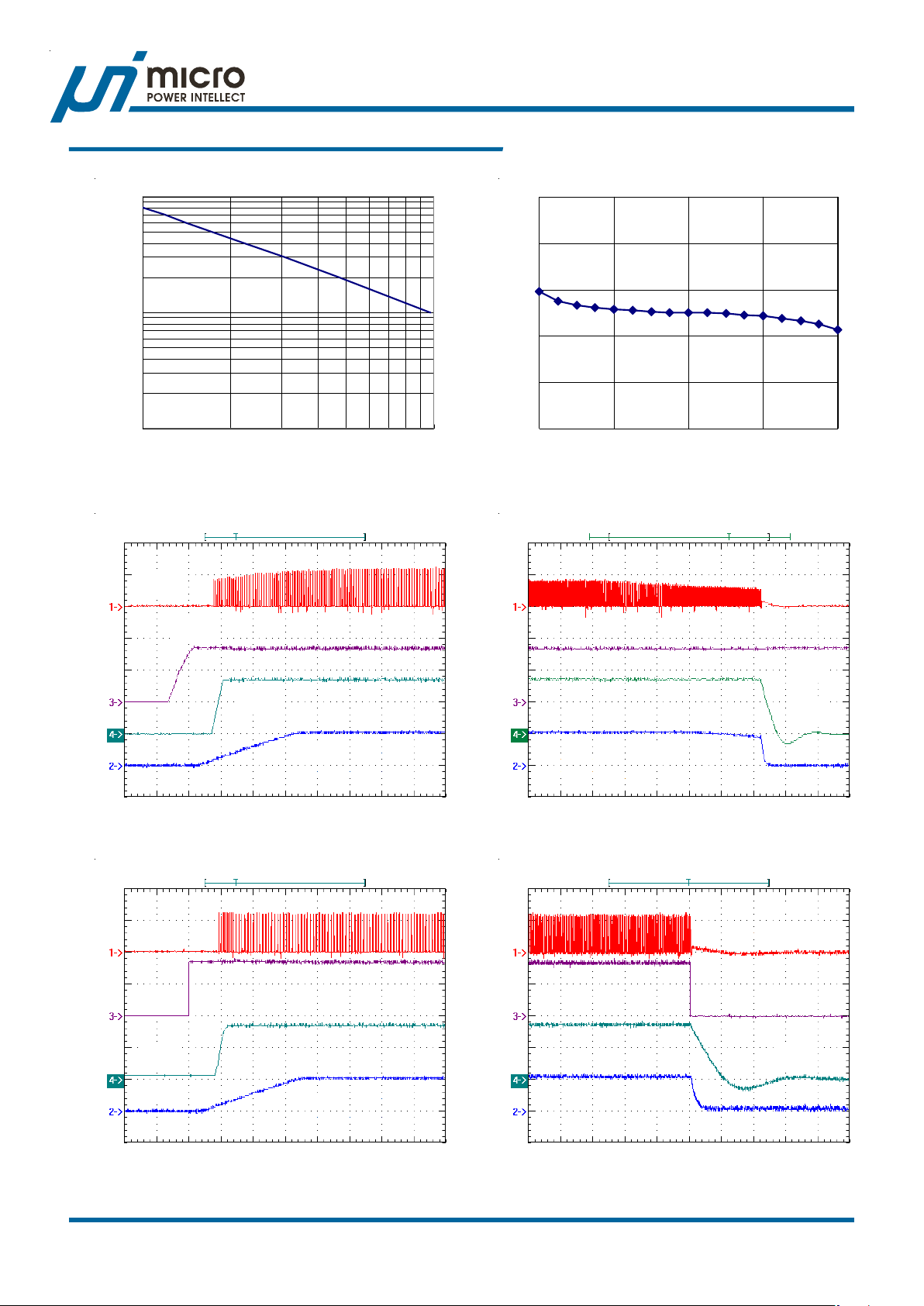
Typical Operation Characteri stics
uP6207
Switching Requency vs. R
1000
100
Switching Frequency (kHz)
10
10 100
Power On Waveforms
PHASE1
(10V/Div)
EN
(5V/Div)
RRT (kΩ)
RT
Switching Frequency vs. Temperature
310
306
302
298
294
Switching Frequency (kHz)
290
-40 0 40 80 120
Junction Temperature (OC)
Power Off Waveforms
PHASE1
(10V/Div)
PHASE1
(10V/Div)
EN
(5V/Div)
V
OUT
(1V/Div)
SS
(5V/Div)
V
OUT
(1V/Div)
SS
(5V/Div)
Time (2.5ms/Div)
I
= 60A
OUT
T urn On Waveforms
SS
(5V/Div)
Time (200us/Div)
I
= 60A
OUT
T urn Off W aveforms
SS
(5V/Div)
EN
(5V/Div)
V
OUT
(1V/Div)
PHASE1
(10V/Div)
EN
(5V/Div)
V
OUT
(1V/Div)
Time (2.5ms/Div)
I
= 60A
OUT
uPI Semiconductor Corp., http://www.upi-semi.com
Rev. P00, File Name: uP6207-DS-P0000
Time (100us/Div)
I
= 60A
OUT
13
Page 14
Preliminary
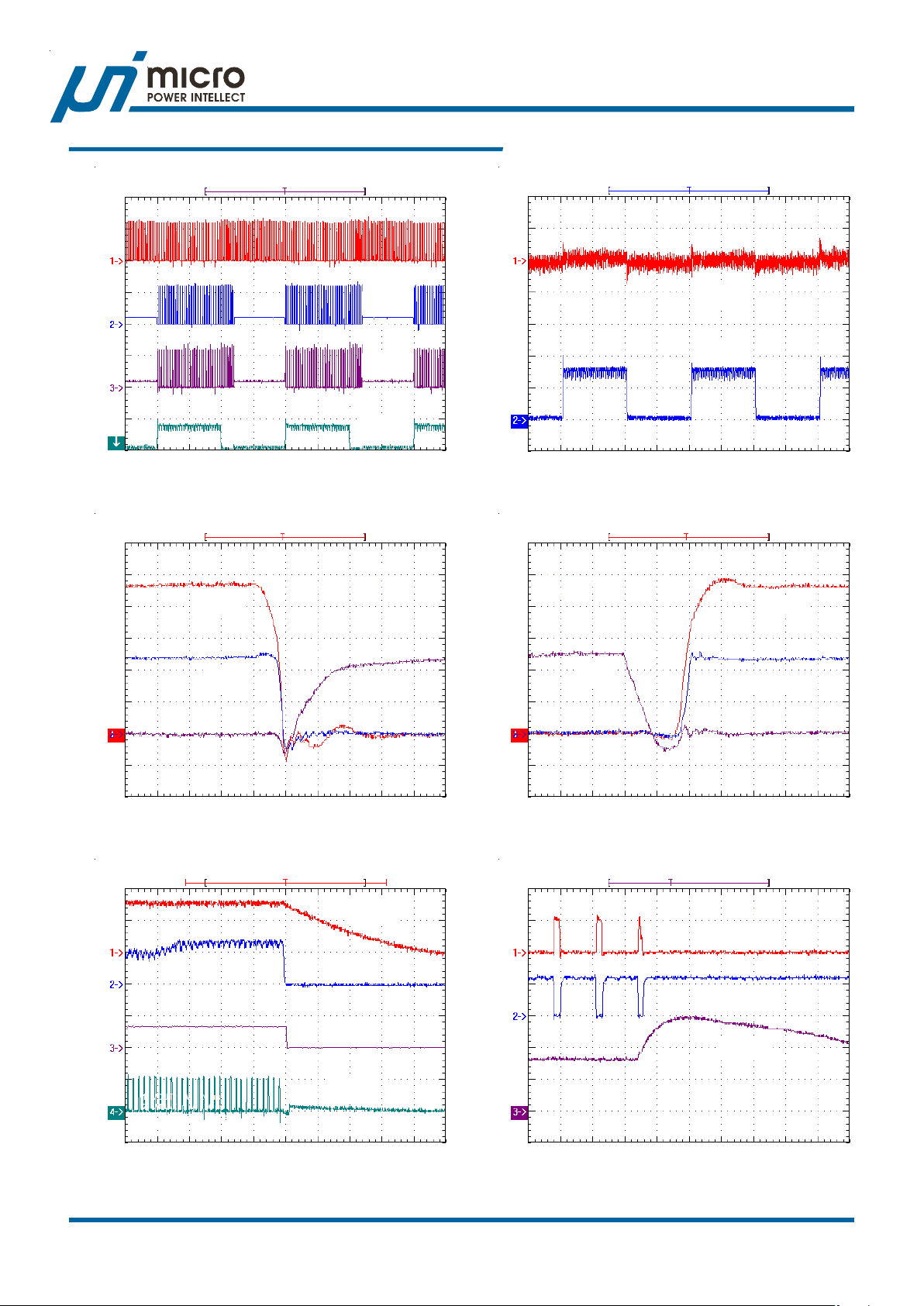
Typical Operation Characteri stics
uP6207
Automatic PSI Operation
Time (2.5ms/Div)
I
= 0A To 60A
OUT
Gate Waveforms
UGATE
(5V/Div)
PHASE1
(10V/Div)
PHASE2
(10V/Div)
PHASE3
(10V/Div)
V
IMAX
(1V/Div)
Tr ansient Re sponse
V
OUT
(50mV/Div)
V
IMAX
(0.5V/Div)
Time (2.5ms/Div)
I
= 0A To 60A
OUT
Gate Waveforms
UGATE
(5V/Div)
PHASE
(5V/Div)
Time (50ns/Div)
I
= 60A
OUT
Over Current Protection
(1V/Div)
V
IMAX
(1V/Div)
VR_RDY
(5V/Div)
PHASE1
(10V/Div)
LGATE
(5V/Div)
V
OUT
LGATE
(5V/Div)
Time (50nus/Div)
I
= 60A
OUT
Over Voltage Protection
PHASE1
(10V/Div)
(10V/Div)
(0.5V/Div)
PHASE
(5V/Div)
LGATE
FB
Time (20us/Div)
uPI Semiconductor Corp., http://www.upi-semi.com
Rev. P0000, File Name: uP6207-DS-P0000
Time (0.5us/Div)
FB Short Circuit to V
OUT
14
Page 15

Preliminary
A
pplication I nformation
This page is intentionally left blank a nd will be update later .
uP6207
uPI Semiconductor Corp., http://www.upi-semi.com
Rev. P00, File Name: uP6207-DS-P0000
15
Page 16
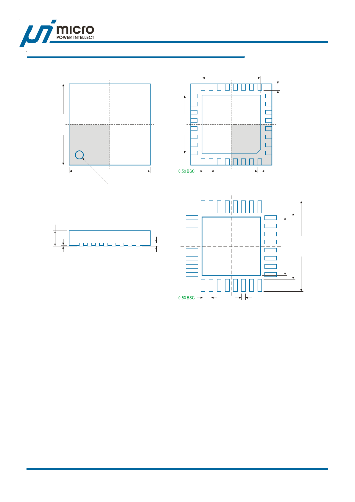
Preliminary
VQF N5x5 - 32L Package
3.55 - 3.65
uP6207
Packag e I nformation
0.35 - 0.45
0.80 - 1.00
0.0 - 0.05
4.90 - 5.10
4.90 -54.10
3.55 - 3.65
0.18 - 0.30
Bottom View - Exposed Pad
Pin 1 mark
3.55 - 3.65
4.05 - 4.15
5.55 - 5.65
0.20 BSC
0.20 - 0.30
Recommended Solder Pad Pitch and Dimensions
Note
1.Package Outline U nit Description:
BSC: Basic. Re presents theoretical exa ct dimen sion or dimen sion target
MIN: Minimum dimension specified.
MAX: Maximum dimension specified.
REF: Reference. Represents dimension f or reference use only . This value is not a device specification.
TYP . Typical. Provided a s a general value. This value is not a device spe cification.
2.Dimensions in Millimeters.
3.Drawing not to scale.
4.These dimensions no not include mold fla sh or protrusion s. Mold fla sh or protrusions shell not exceed 0.15mm.
uPI Semiconductor Corp., http://www.upi-semi.com
Rev. P0000, File Name: uP6207-DS-P0000
16
 Loading...