

Page 1
uP6201A/B
A
Compact Dual-Phase
Synchronous-Rectified Buck Controller
General Description
The uP6201A/B is a compact dual-phase synchronousrectified Buck controller specifically designed to deliver high
quality output voltage for high power applications. This part
is capable of delivering up to 60A output current thanks to
its embedded bootstrapped drivers that support 12V + 12V
driving capability. The uP6201A/B features configurable gate
driving voltage for maximum efficiency and optimal
performance. The built-in bootstrap diode simplifies the
circuit design and reduces external part count and PCB
space.
The output voltage is precisely regulated to internal 0.6V
or external reference voltage from 0.4V to 2.5V. The
uP6201A/B adopts DCR current sensing technique for
channel current balance, over current protection, droop
control, and output current indication. The uP6201A/B offers
a regulated 5V voltage with 20mA output current capability
for other peripheral circuitry.
A MODE pin programs single- or two- phase operation
making the uP6201A/B ideally suitable for dual power input
applications like PCIE interfaced graphic cards.
This part features comprehensive protection functions
including over current protection, input/output under voltage
protection, over voltage protection and over temperature
protection.
Other features include adjustable soft start, adjustable
operation function, quick response to step load transient,
and power OK. With aforementioned functions, this part
provides customers a compact, high efficiency, wellprotected and cost-effective solutions. This part comes to
QFN4x4-24L package.
Features
Operate with 4.5V ~13.2V Supply Voltage
Selectable External or Internal 0.6V Reference
Support Single- and Two- Phase Operation
5VCC with 20mA Output Current Capability
±±
±2.0% Over Line Voltage and Temperature
±±
Simple Single-Loop Voltage-Mode Control
12V Bootstrapped Drivers with Internal
Bootstrap Diode
DCR Current Sensing
Adjustable Operation Frequency form 50kHz to
1MHz Per Phase
External Compensation
Adjustable Over Current Protection and Output
Current Indication
External Reference
Adjustable Soft Start
QFN4x4-24L Package
RoHS Compliant and 100% Lead (Pb)-Free
pplications
Middle-High End GPU Core Power
High End Desktop PC Memory Core Power
Low Output Voltage, High Power Density DC-DC
Converters
Voltage Regulator Modules
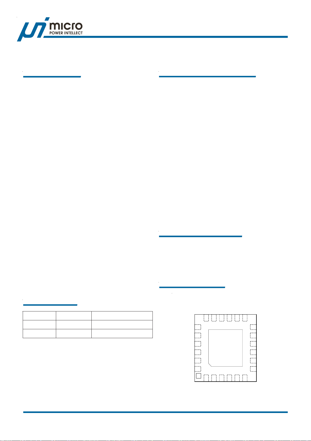
Pin Configuration
Ordering Information
rebmuNredrOepyTegakcaPkrameR
QA1026PuL42-4x4NFQnoitcnuFpoorDhitW
QB1026PuL42-4x4NFQnoitcnuFpoorDtuohtiW
Note: uPI products are compatible with the current IPC/
JEDEC J-STD-020 and RoHS requirements. They are 100%
matte tin (Sn) plating and suitable for use in SnPb or Pbfree soldering processes.
uPI Semiconductor Corp., http://www.upi-semi.com
Rev. 03, August 2007
PHASE2
VCCDRV
VCC
LGATE1
PHASE1
UGATE2
POK5VCC
REFIN
BOOT2
17 16 1518
19
20LGATE2
21
22
23
24
UGATE1
PGND
4321
BOOT1
uP6201A/B
AGND
FB
SS/ENMODE
14
13
12
COMP
11 RT
IOUT
10
9
CSP2
CSN2
8
7
CSN1
5
6
CSP1
1
Page 2
V
= 10.8~13.2V
IN
C
30
uP6201A/B
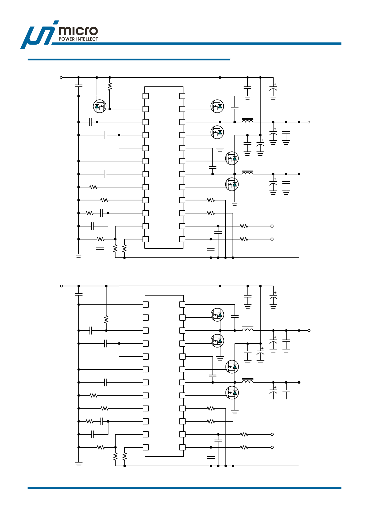
Typical Application Circuit
R
30
C
21
C
20
V
= 10.8~13.2V
IN
C
30
MODE
5
VCCDRV
C
31
C
32
C
33
R
33
R
34
R
35
C
34
C
35
R
36
R
37
21
VCC
22
5VCC
3 23
REFIN
15
AGND
4
SS/EN
RT
11
IOUT
10
COMP
12
FB
13
POK
16
R
38
uP6201A/B
2
1
24
17
18
1914
20
8
7
9
6
BOOT1
UGATE1
PHASE1
LGATE1
BOOT2
UGATE2
PHASE2
LGATE2
CSN2
CSN1
CSP2
CSP1
C
10
Q
1
L
1
C23C
22
C25C
Q
2
C
R
40
R
41
C
40
C
41
Q3L
11
Q
24
2
C27C
26
4
PHASE2
R
42
PHASE1
R
43
V
OUT
A. 9V Drive Using External Regulator
C
21
C
20
MODE
5
R
C
R
R
30
31
C
32
C
33
33
R
34
35
C
34
C
35
R
36
VCCDRV
R
37
21
VCC
22
5VCC
3 23
REFIN
15
AGND
4
SS/EN
RT
11
IOUT
10
COMP
12
FB
13
POK
16
R
38
uP6201A/B
2
1
24
17
18
1914
20
8
7
9
6
BOOT1
UGATE1
PHASE1
LGATE1
BOOT2
UGATE2
PHASE2
LGATE2
CSN2
CSN1
CSP2
CSP1
C
10
Q
1
L
1
C23C
22
C25C
Q
2
C
R
40
R
41
C
40
C
41
Q3L
11
Q
24
2
C27C
26
4
PHASE2
R
42
PHASE1
R
43
V
OUT
B. 12V Drive
uPI Semiconductor Corp., http://www.upi-semi.com
Rev. 03, August 2007
2
Page 3
V
= 3.3 ~ 13.2V
IN
uP6201A/B
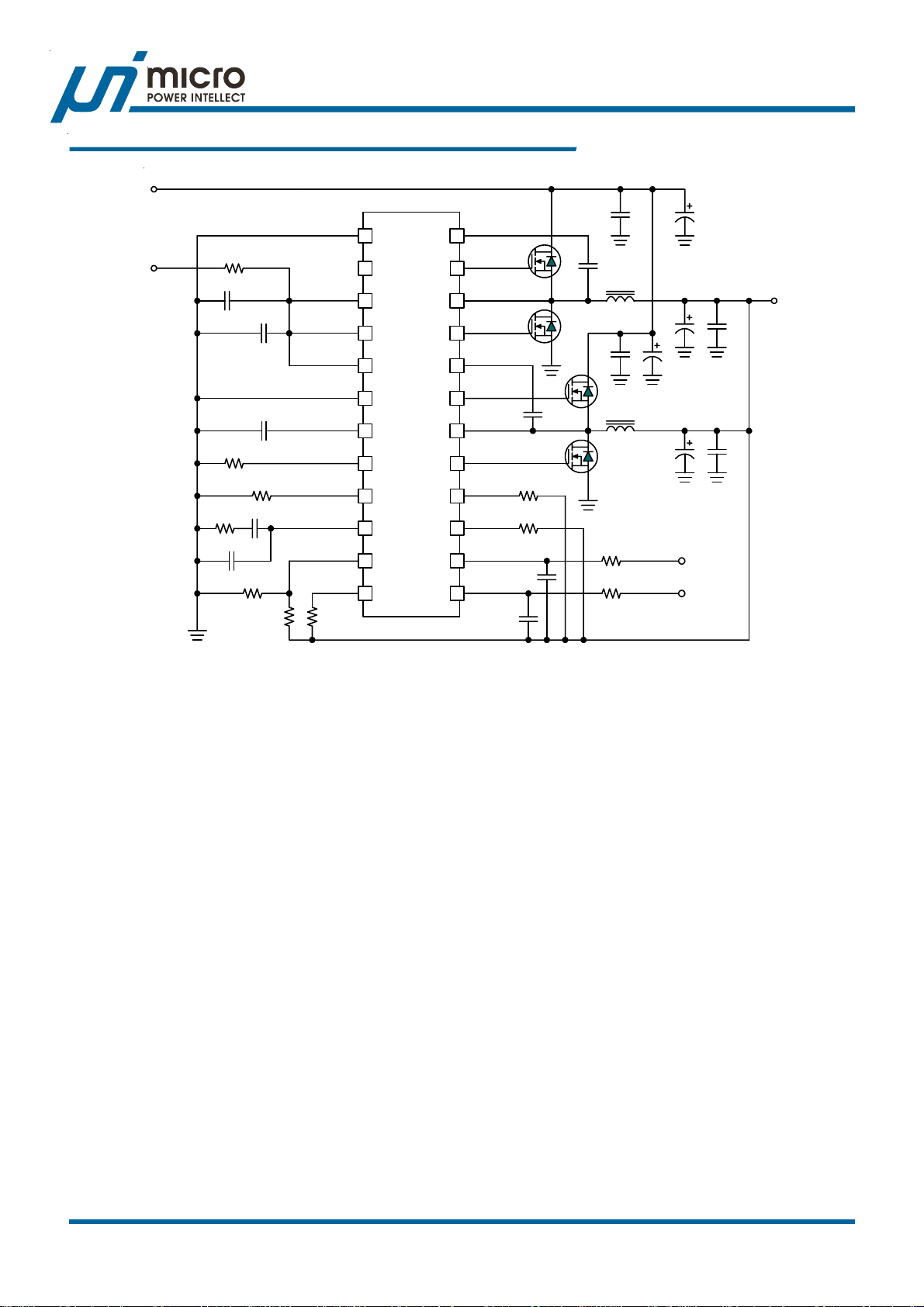
Typical Application Circuit
C
21
C
20
MODE
5
5V
R
30
C
31
C
32
C
33
R
33
R
34
R
35
C
34
C
35
R
36
VCCDRV
R
37
21
VCC
22
5VCC
3 23
REFIN
15
AGND
4
SS/EN
RT
11
IOUT
10
COMP
12
FB
13
POK
16
R
38
uP6201A/B
2
1
24
17
18
1914
20
8
7
9
6
BOOT1
UGATE1
PHASE1
LGATE1
BOOT2
UGATE2
PHASE2
LGATE2
CSN2
CSN1
CSP2
CSP1
C
10
Q
1
L
1
C23C
22
C25C
Q
2
C
R
40
R
41
C
40
C
41
Q3L
11
Q
24
2
C27C
26
4
PHASE2
R
42
PHASE1
R
43
V
OUT
C. 5V Drive
uPI Semiconductor Corp., http://www.upi-semi.com
Rev. 03, August 2007
3
Page 4
.oNemaNniPnoitcnuFniP
n
11ETAGU
21TOOB
3CCV5
uP6201A/B
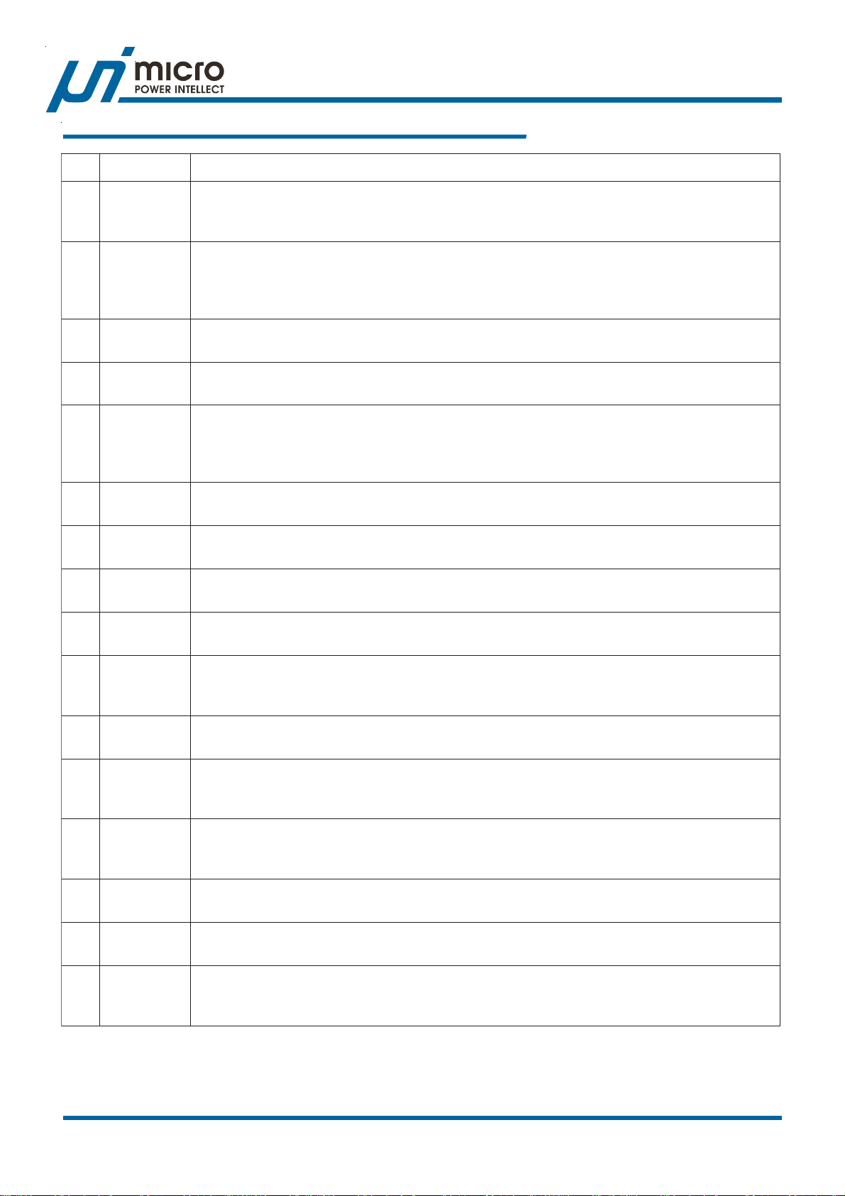
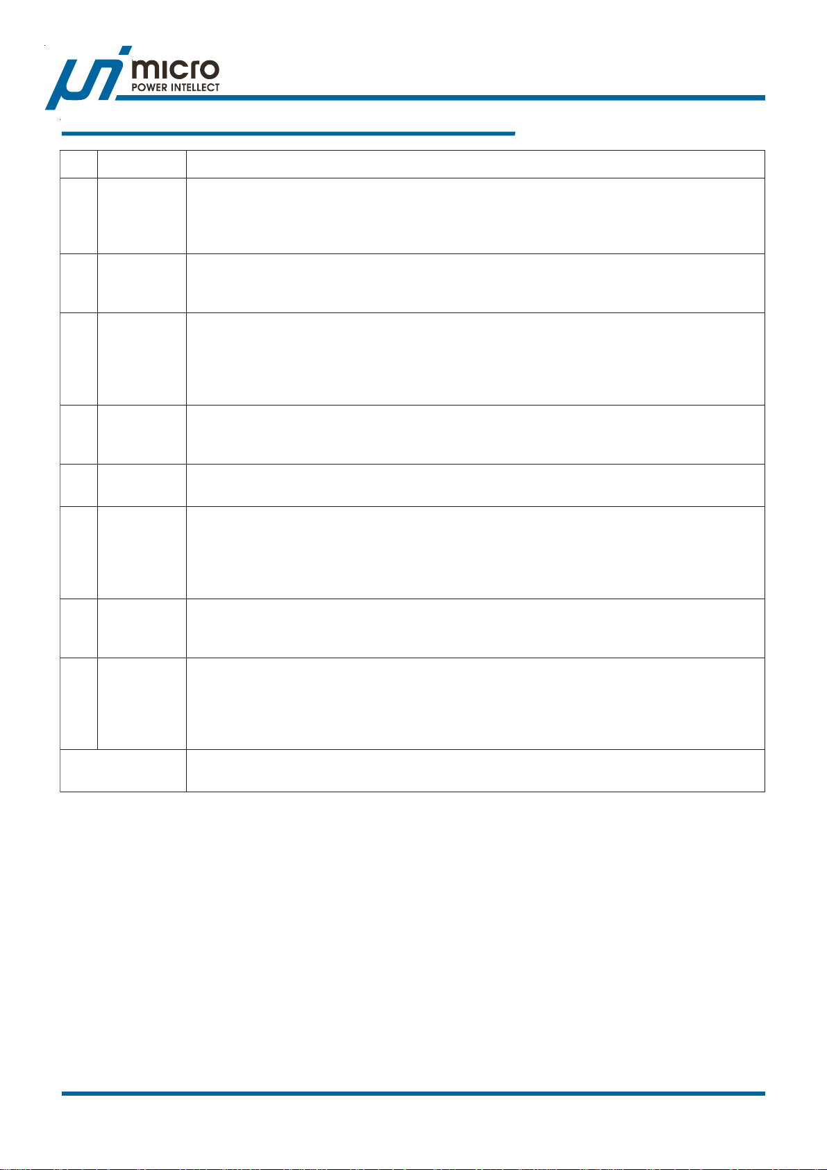
Functional Pin Descriptio
.1lennahCroftuptuOrevirDetaGreppU .TEFSOMreppufoetagehtotnipsihttcennoC
ehtnehwenimretedotyrtiucricnoitcetorphguorht-toohsevitpadaehtybderotinomsinipsihT
.ffodenrutsahTEFSOMreppu
ylppuSpartstooB partstoobehttcennoC.1lennahcforevirdetagreppugnitaolfehtrof
rofseulavlacipyT.TEFSOMreppuehtnonrutotegrahcehtsedivorproticapacpartstoob C
ehT.tiucricpartstoobamrofotnip1ESAHPehtdnanip1TOOBneewteb
TOOB
Croticapac
TOOB
CtahterusnE.Fu74.0otFu1.0morfegnar
TOOB
.CIehtraendecalpsi
.tuptuOrotalugeRlanretnI lanretxednasaiblanretnirofrotalugerraenilfoniptuptuoehtsisihT
.Am02siytilibapactnerructuptuoehT.egasu
4DNGA
5EDOM
61PSC
71NSC
82NSC
92PSC
01TUOI
11TR
21PMOC
.CIehtrofdnuorGlangiS sihteiT.nipsihtottcepserhtiwderusaemeraslevelsegatlovllA
.elbaliavanoitcennocecnadepmitsewolehthguorhtenalp/dnalsidnuorgehtotnip
.noitceleSesahPnoitarepO .noitarepoesahp-owtstesV4.0nahtrewolnipsihtgnilluP
ecnO.2esahpselbasiddnanoitarepoesahp-elgnisstesV4.1nahtrehgihnipsihtgnilluP
NE/SSelggototderiuqersitI.dehctalsiedomnoitarepoeht,edomesahp-elgnisnidetarepo
.CIehtteserotnipCCV5ro
.1MGgnisneStnerruCfotupnIevitisoP rotcudniehtsesnes1NSChtiwdeinapmocnipsihT
.krowtenCRnahguorht1lennahcfotnerruc
.1MGgnisneStnerruCfotupnIevitageN rotcudniehtsesnes1PSChtiwdeinapmocnipsihT
.krowtenCRnahguorht1lennahcfotnerruc
.2MGgnisneStnerruCfotupnIevitageN rotcudniehtsesnes2PSChtiwdeinapmocnipsihT
.krowtenCRnahguorht2lennahcfotnerruc
.2MGgnisneStnerruCfotupnIevitisoP rotcudniehtsesnes2NSChtiwdeinapmocnipsihT
.krowtenCRnahguorht2lennahcfotnerruc
.noitacidnItnerruCtuptuO htiwnipsihttcennoC.leveltnerructuptuoehtsetacidninipsihT
edicedoslarotsiserehT.noitacidnitnerructuptuoehtfotneiciffeocehttesotdnuorgotrotsiser
)ylnOA1026Pu(lortnocpoordfoecnadepmituptuoeht
.gnitteSycneuqerFnoitarepO ehttesotDNGAdnanipsihtneewtebrotsiseragnitcennoC
.ycneuqerfnoitarepo
.tuptuOreifilpmArorrE tupnignitrevni-nonehtdna)AE(reifilpmarorreehtfotuptuoehtsisihT
-egatlovehtetasnepmocotnipBFehthtiwnoitanibmocninipsihtesU.srotarapmocMWPehtfo
.retrevnocehtfopoolkcabdeeflortnoc
.egatloVkcabdeeF morfredividrotsiserA.reifilpmarorreehtottupnignitrevniehtsinipsihT
31BF
41NE/SS
.tuptuOtratStfoS .lavretnitratstfosehttesotDNGAotnipsihtmorfroticapacatcennoC
51NIFER
.noitacidnIKOrewoP segatlovehtfosutatsehtetacidniotdesutuptuoniardneponasiKOP
61KOP
.sdnetrats
uPI Semiconductor Corp., http://www.upi-semi.com
Rev. 03, August 2007
.tupnIecnerefeRlanretxE ecnereferlanretxefI.egatlovecnereferlanretxefoniptupnisisihT
ehthtiwnoitanibmocninipsihtesU.egatlovnoitalugerehttesotdesusiDNGAottuptuoeht
.retrevnocehtfopoolkcabdeeflortnocegatlovehtetasnepmocotnipPMOC
.B/A1026PuehtnwodstuhsV5.0otnwodnipsihtwolgnilluP
.ecnereferV6.0lanretnirofCCV5otnipsihttcennoc,elbaliavatonsiegatlov
VfiecnadepmihgihoglliwKOP.nipBFdnanipSSno
BF
tfosretfaegatlovecnereferfo%570>
4
Page 5
.oNemaNniPnoitcnuFniP
n
712TOOB
812ETAGU
912ESAHP
022ETAGL
ylppuSpartstooB partstoobehttcennoC.2lennahcforevirdetagreppugnitaolfehtrof
uP6201A/B
Functional Pin Descriptio
partstoobehT.tiucricpartstoobamrofotnip2ESAHPehtdnanip2TOOBneewtebroticapac
CrofseulavlacipyT.TEFSOMreppuehtnonrutotegrahcehtsedivorproticapac
CtahterusnE.Fu74.0otFu1.0
TOOB
.2lennahCroftuptuOrevirDetaGreppU .TEFSOMreppufoetagehtotnipsihttcennoC
.ffodenrutsahTEFSOMreppu
.2lennahCrofedoNhctiwS ehtdnaTEFSOMreppuehtfoecruosehtotnipsihttcennoC
.2lennahCroftuptuOrevirDetaGrewoL sihT.TEFSOMrewolfoetagehtotnipsihttcennoC
.ffodenrutsahTEFSOM
.CIehtraendecalpsi
TOOB
.metsysylppusrewopaninommocsihcihwegatlovtneisnartevitagenecuder
morfegnar
ehtnehwenimretedotyrtiucricnoitcetorphguorht-toohsevitpadaehtybderotinomsinipsihT
oslasinipsihT.revird2ETAGUehtrofknisehtsadesusinipsihT.TEFSOMrewolehtfoniard
reppuehtnehwenimretedotyrtiucricnoitcetorphguorht-toohsevitpadaehtybderotinom
otdednemmocersidnuorgdnanipsihtneewtebedoidykttohcSA.ffodenrutsahTEFSOM
rewolehtnehwenimretedotyrtiucricnoitcetorphguorht-toohsevitpadaehtybderotinomsinip
12VRDCCV
22CCV
321ETAGL
421ESAHP
.rotalugeRraeniLlanretxErofrevirD raenillanretxetahtroftuptuoevirdehtsinipsihT
.tnemelessapehtsarotsisnartSOMN/NPNfoetag/esabehtotnipsihttcennoC.rotaluger
.egatloVylppuS asedivorptnemelessaplanretxednanipVRDCCVhtiwgnolanipsihT
tiucricpartstoobehtdna,srevirdetagrewoleht,B/A1026PuehtrofylppussaibV8detaluger
ehtfienolaegatlovylppusV2.31~5.4delpuoced-llewaeviecernacnipsihT.srevirdreppurof
ehtottxenroticapaccimarecaybdessapybsinipsihttahterusnE.nepotfelsinipVRDCCV
.CI
.1lennahCroftuptuOrevirDetaGrewoL sihT.TEFSOMrewolfoetagehtotnipsihttcennoC
rewolehtnehwenimretedotyrtiucricnoitcetorphguorht-toohsevitpadaehtybderotinomsinip
.ffodenrutsahTEFSOM
.1lennahCrofedoNhctiwS ehtdnaTEFSOMreppuehtfoecruosehtotnipsihttcennoC
oslasinipsihT.revirdETAGUehtrofknisehtsadesusinipsihT.TEFSOMrewolehtfoniard
reppuehtnehwenimretedotyrtiucricnoitcetorphguorht-toohsevitpadaehtybderotinom
otdednemmocersidnuorgdnanipsihtneewtebedoidykttohcSA.ffodenrutsahTEFSOM
.metsysylppusrewopaninommocsihcihwegatlovtneisnartevitagenecuder
daPdesopxE
DNGP
.dnuorGrewoP iT noitcennocecnadepmitsewolehthguorhtenalp/dnalsidnuorgehtotnipsihte
.elbaliava
uPI Semiconductor Corp., http://www.upi-semi.com
Rev. 03, August 2007
5
Page 6
uP6201A/B
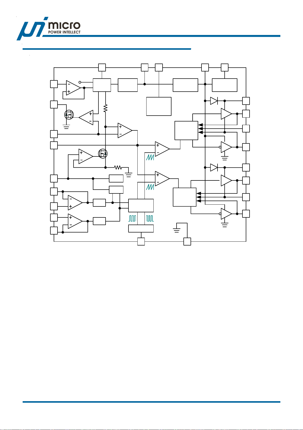
Functional Block Diagram
REFIN
POK
FB
COMP
IOUT
CSN1
CSP1
CSP2
CSN2
15
16
13
12
10
SS/EN
0.6V
Soft Start
V
75%V
REF
V
7
6
9
8
GM1
S/H
S/H
GM2
POR
REF
R
REFX
10R
OCP
SUM
Error
Amplifier
Current
Balance
Oscillator
5VCC BUSEN
514
3
Operation
Phase
Selection
Comparators
Internal
Regulator
Gate
Control
Logic
PWM1
PWM
PWM2
Gate
Control
Logic
VCC
22
VCCDRV
21
External
Regulator
2
1
24
23
17
18
19
20
BOOT1
UGATE1
PHASE1
LGATE1
BOOT2
UGATE2
PHASE2
LGATE2
11
RT
uP6201A
4
GND
uPI Semiconductor Corp., http://www.upi-semi.com
Rev. 03, August 2007
6
Page 7
The uP6201A/B is a compact dual-phase synchronousrectified Buck controller specifically designed to deliver high
quality output voltage for high power applications. This part
is capable of delivering up to 60A output current thanks to
its embedded bootstrapped drivers that support 12V + 12V
driving capability. The built-in bootstrap diode simplifies the
circuit design and reduces external part count and PCB
space.
The output voltage is precisely regulated to internal 0.6V
or external reference voltage from 0.4V to 2.5V. The
uP6201A/B adopts DCR current sensing technique for
channel current balance, over current protection, droop
control, and output current indication. The uP6201A/B offers
5VCC with 20mA output current capability for other
peripheral circuitry.
uP6201A/B
Functional Description
= 10.8~13.2V
V
IN
VCCDRV
VCC
5VCC
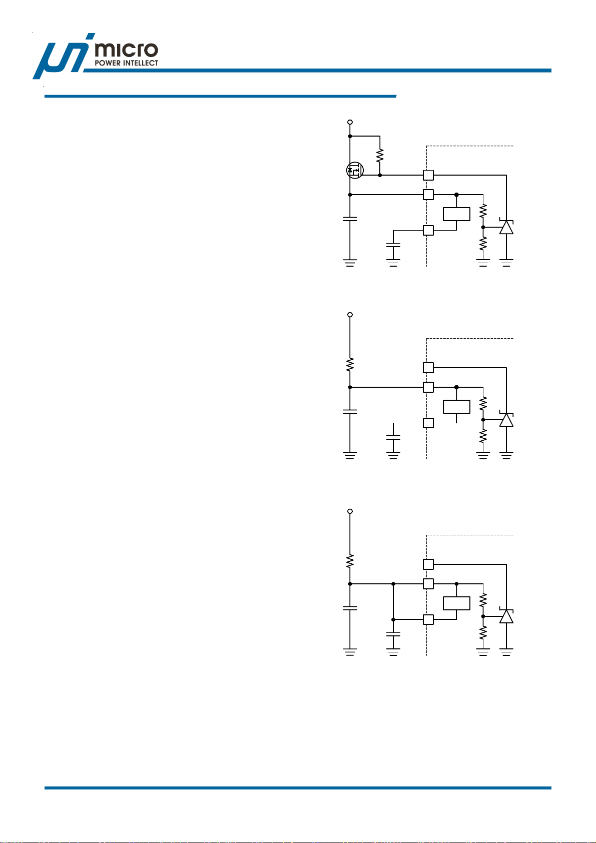
Figure 1. 9V Drive Application
uP6201A/B
21
22
LDO
3
This part features comprehensive protection functions
including over current protection, input/output under voltage
protection, over voltage protection and over temperature
protection.
Other features include internal soft start, adjustable
operation function, quick response to step load transient,
power OK and external reference input. With aforementioned
functions, this part provides customers a compact, high
efficiency, well-protected and cost-effective solutions. This
part comes QFN 4x4_24L package.
External VCC and Internal 5VCC Regulator
The uP6201A/B provides flexible gate driving voltage for
maximum efficiency and optimal performance. The VCC
pin powers the uP6201A/B control circuit, the lower gate
drivers and the bootstrap circuit for the higher gate drivers.
A linear regulator regulates VCC at 9V as shown in Figure
1. Connect VCCDRV pin to the base/gate of the external
NPN/NMOS transistor and VCC pin to the emitter/source
to form a linear regulator. Ensure that the ceramic bypass
capacitor is placed next to the IC.
An internal linear regulator regulates VCC input to a 5VCC
voltage for internal control logic circuit if VCC is higher
than 7V. This linear regulator is designed to support up to
20mA output current for peripheral circuits. Place an 1uF
ceramic capacitor next to the 5VCC pin to decouple this
voltage.
= 10.8~13.2V
V
IN
VCCDRV
VCC
5VCC
uP6201A/B
21
22
LDO
3
Figure 2. 12V Drive Application
= 4.5~5.5V
V
IN
VCCDRV
VCC
5VCC
uP6201A/B
21
22
LDO
3
Figure 2 shows the application where 12V gate voltage is
used. When VCCDRV is left open, VCC pin can receive a
well decoupled supply input of 4.5~13.2V. However, if V
is lower than 5.5V, the dropout voltage of the internal
regulator may cause 5VCC too low for normal operation.
Tie 5VCC to VCC directly for the applications where VCC
is under 5.5V as shown in Figure 3.
uPI Semiconductor Corp., http://www.upi-semi.com
Rev. 03, August 2007
Figure 3. 5V Drive Application
Bootstrap diodes are embedded to facilitates PCB design
IN
and reduce the total BOM cost. No external Schottky diode
is required. The uP6201A/B integrates MOSFET gate
drives that are powered from the VCC pin and support
12V+12V driving capability. Converters that consist of
uP6201A feature high efficiency without special
consideration on the selection of MOSFETs.
7
Page 8
uP6201A/B
Functional Description
Note that the built-in bootstrapping diode is not a
Schottky diode having higher forward bias voltage.
When using 5V driving voltage, external Schottky
diode is recommended for bootstrapping diode.
Power On Reset and Initialization
The uP6201A/B continuously monitors 5VCC for power
on reset (POR) to ensure the supply voltage is high enough
for normal operation of the device. The POR threshold level
is typically 4.2V at 5VCC rising.
Operation Phase Selection
The uP6201A/B supports single- or two- phase operation.
Pulling the MODE pin lower than 0.4V sets two-phase
operation. Pulling the MODE pin higher than 1.4V sets
single-operation. Once operated in single-phase mode, the
operation phase is latched and can only be reset by toggle
5VCC or SS/EN pin. This feature is important for PCIE
interfaced graphic cards where neither bus power nor
external power is capable of delivering full load current.
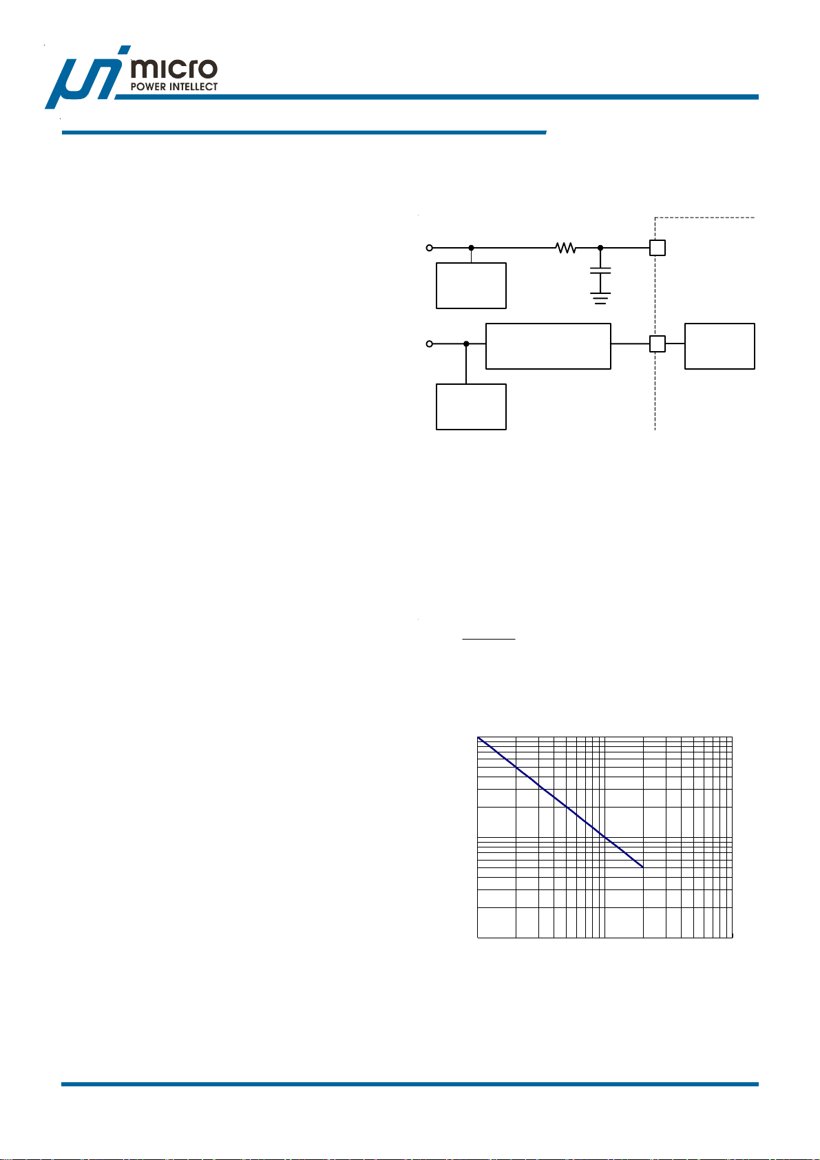
Configure the converter as shown in Figure 4. Power the
phase 1 converter by PCIE bus power and power the phase
2 converter by external power. If the external power code
is not plugged into the socket, the External Power Detection
will set MODE pin high and the uP6201A/B operates in
single phase mode. The uP6201A/B could provides limited
current to GPU for required operation when external power
is not plugged.
Two-phase operation will making the phase 2 converter acts
like an boost converter if the external power is not available,
boosting the output voltage to the input voltage. The
relationship between input voltage and output voltage is
governed by conventional boost converter equation. Offset
of the current balance function may make the duty cycle of
phase 2 converter smaller than that of phase 1 converter.
This results in external power higher than 15V that may
damage the input capacitors and other devices. Figure 4
configuration turns off phase 2 converter when the external
power is not available, thus eliminates the possibility of
over voltage on input capacitors and other devices of the
phase 2 converter.
otherwise external reference voltage is selected. Once
selected, the reference source is fixed and can only be
programmed at next POR.
PCIE +12V
Phase 1
Converter
Ext. +12V
Phase 2
Converter
External Power Detection
Ext. Pwr Plugged = 0
Ext. Pwr Not Plugged = 1
VCC
MODE
22
5
uP6201A/B
Operation
Phase
Selection
Figure 4. Single/Two Phase Operation
Tie REFIN voltage to 5VCC to select internal reference when
POR. If the external reference voltage is higher than 2.5V
before POR, it may cause uP6201A/B to select internal
0.6V reference voltage and should be avoided.
Oscillation Frequency Programming
A resistor RRT connected to RT pin programs the oscillation
frequency as:
=
10000
RT
)k(R
Ω
(kHz)
f
OSC
Figure 5 shows the relationship between oscillation
frequency and RRT.
1000
100
Note that when operated in single phase, the rated
current is reduced to one half of normal level.
Continuous demanding high current may damage the
converter.
Reference Voltage Selection
The uP6201A/B features selectable internal or external
reference voltage. The REFIN voltage level is checked at
POR to select the desired reference voltage. Internal 0.6V
reference voltage is selected if V
uPI Semiconductor Corp., http://www.upi-semi.com
Rev. 03, August 2007
REFIN
> V
- 0.8V at POR,
CC5
Switching Frequency (kHz)
10
10 100 1000
RRT (kohm)
Figure 5. Switching Frequency vs. RRT.
8
Page 9
uP6201A/B
Functional Description
Soft Start and Power OK
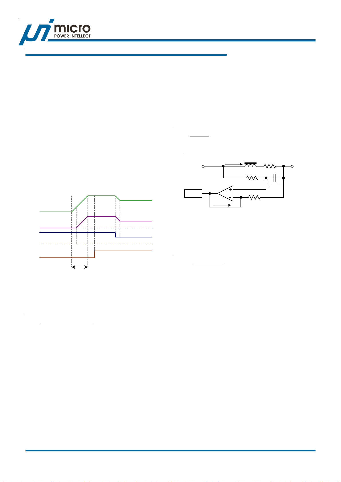
Once POR releases, the uP6201A/B initiates its soft start
cycle. Figure 6 shows the softstart cycle with external
reference voltage. A 10uA current charges the soft start
capacitor CSS making its voltage VSS linearly ramp up. The
VSS clamps reference voltage V
with a MOSFET
REF
threshold voltage at non-inverting input of the error amplifier.
Accordingly, the output voltage will softly ramp up and draw
minimum inrush current from the power bus.
The uP6201A/B features pre-bias start-up capability. If the
output voltage is pre-biased with a voltage, say V
BIAS
, that
accordingly makes VFB higher than reference voltage
ramping V
. The error amplifier keeps V
REF
lower than
COMP
the valley of the sawtooth waveform and makes PWM
comparators output low until the ramping V
catches up
REF
the feedback voltage. The uP6201A/B keeps both upper
and lower MOSFETs off until the first pulse takes place.
SS/EN
V
REF
REFIN
POK
t
SS
Figure 6. Timing Diagram of Soft Start Interval.
The uP6201A/B claims soft start end when V
up V
and set POK to high impedance output if no fault
REFIN
catches
REF
conditions are detected. The total soft start time with external
reference voltage is about
+
=
t
SS
REFINSS
uA10
)V8.0V(C
where 0.8V accounts for the delay time caused by the
MOSFET threshold voltage. When internal 0.6V reference
voltage is used, simply take V
= 0.6V into the above
REFIN
equation.
When external reference voltage changes, the slew rate of
V
is also limited by the soft start mechanism.
REF
Consequently, this results in a smooth output voltage
transition during external reference voltage change. The soft
start also acts as the timer during OCP and UVP as
described in the later sections.
Channel Current Sensing
The uP6201A/B extracts phase currents by parasitic DCR
of the inductors for channel current balancing, droop tuning,
and over current detecting. An RC network is paralleled to
the inductor for current sensing as shown in Figure 7 where
DCR is the parasitic resistance. The VC across the capacitor
equals to V
= IL x DCR across the DCR of the inductor if
DCR
the time constants match: RC = L/DCR.
The GM amplifier will source a current source I
R
to virtually short its two inputs. Consequently I
CSN
CSN
= VC/
CSN
sampled and held as:
IDCRI×
CSN
=
V
R
PHASE
CSN
L
I
L
DCRL
V
OUT
CR
S/H
I
GM
CSN
R
CSN
V
C
Figure 7. DCR Current Sensing Scheme
The sourcing capability of the GM amplifier is 100uA. It is
recommended to scale I
= 30uA at rated inductor current.
CSN
Take a 60A converter for example. Assume DCR = 2mΩ,
select the sense resistor according to
= k0.2
R
CSN
m2A30
uA30
Ω=
Ω×
Current Balance
The uP6201A/B fine tunes the duty cycle of each channel
for current balance according to the sensed inductor current
signals. If the current of channel 1 is smaller than the current
of channel 2, the uP6201A/B increases the duty cycle of
the corresponding phase to increase its phase current
accordingly, vice verse.
Over Current Protection
The sensed current signals are monitored for over current
protection. The uP6201A/B features both total current OCP
and phase current OCP. If I
the phase current OCP is activated. If I
CSN1
or I
is higher than 80uA,
CSN2
CSN1
+ I
SCN2
is higher
than 120uA, total current OCP is activated.
The uP6201A/B features hiccup and shutdown mode OCP.
If OCP takes place after soft start end, the uP6201A/B turns
off both upper and lower MOSFETs and discharges the C
SS
with a constant current of 10uA. When VSS touches down
0.4V, the uP6201A/B initiates another soft start cycle. The
uP6201A/B shuts down after 4 times hiccups. If the OCP
takes place during soft start cycle, the uP6201A/B turns off
both upper and lower MOSFETs but keeps charging the
CSS with a constant current of 10uA until the soft start end.
is
uPI Semiconductor Corp., http://www.upi-semi.com
Rev. 03, August 2007
9
Page 10
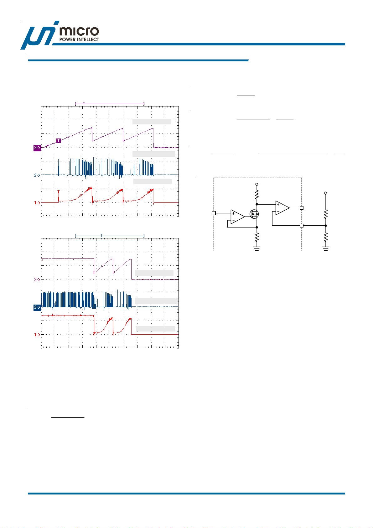
The shutdown status can only be reset by POR function.
Figure 8, and Figure 9 illustrate the OCP behaviors during
soft start and after soft start end respectively.
uP6201A/B
Functional Description
same current and see same voltage drop that is exactly
V
. Consequently,
IOUT
V
VV
REFREFX
IOUT
−=
10
Phase 2 (10V/Div)
V
Figure 8. OCP during Soft Start
SS (1V/Div)
(1V/Div)
OUT
SS (1V/Div)
Finally,
V
IOUT
×
−=
VV
REFREFX
+
=
2R1R
2R
V
IOUT
Figure 10. Load Line Setting
IDCR
×
R2
CSN
−×
V
REFOUT
V
REF
R
OUT
V
10R
REFX
R
×
IOUT
10
IOUT
CSN
Error
Amplifier
××
+××
2RR2
COMP
FB
I
)2R1R(RDCR
OUT
×
10
V
OUT
R1
R2
Phase 2 (10V/Div)
V
(1V/Div)
OUT
Figure 9. OCP after Soft Start End.
Output Current Indication
The sensed current signals are summed and injected into
the IOUT pin for output current indication. A resistor R
connected to this pin scales the voltage V
proportional
IOUT
IOUT
to the output current:
IDCR
×
OUT
V ×
=
IOUT
R2
×
CSN
R
IOUT
Droop Tuning (uP6201A Only)
The IOUT pin also adjusts the load line for droop control as
shown in Figure 10. The V
is the internal 0.6V or external
REF
reference voltage as described in the relative sections. The
V
is the real reference voltage at the non-inverting input
REFX
of the error amplifier. The two well-matched Rs share the
uPI Semiconductor Corp., http://www.upi-semi.com
Rev. 03, August 2007
10
Page 11
uP6201A/B
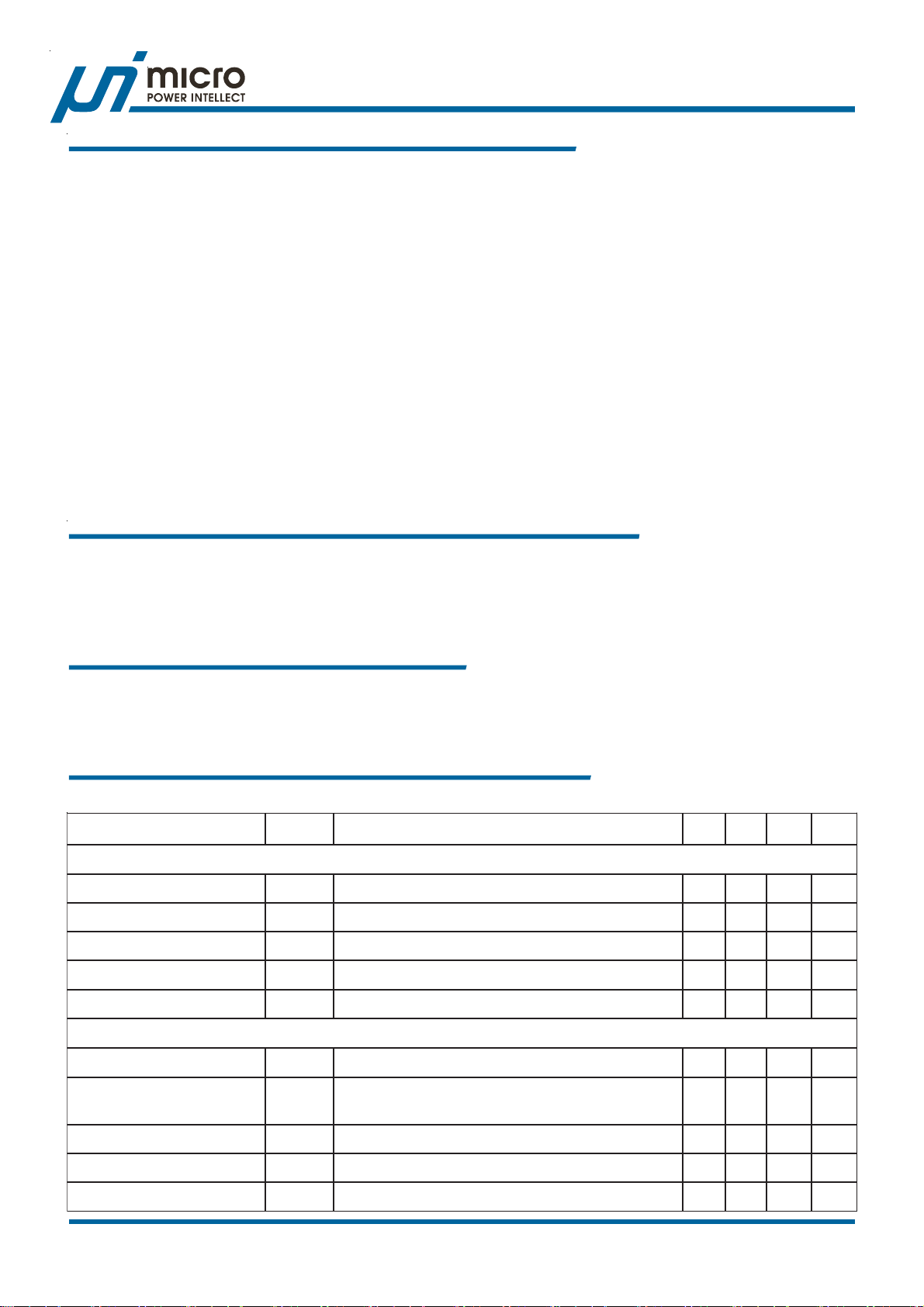
A
g
n
bsolute Maximum Ratin
Supply Input Voltage, VCC (Note 1) ------------------------------------------------------------------------------------------------ -0.3V to +15V
VCCDRV --------------------------------------------------------------------------------------------------------------------------------------- -0.3V to +15V
PHASE to GND
DC ------------------------------------------------------------------------------------------------------------------------------------- -0.3V to 15V
< 200ns ---------------------------------------------------------------------------------------------------------------------------- -5V to 30V
BOOT to PHASE -------------------------------------------------------------------------------------------------------------------------------------- 15V
BOOT to GND
DC ------------------------------------------------------------------------------------------------------------------------- -0.3V to PHASE +15V
< 200ns -------------------------------------------------------------------------------------------------------------------------- -0.3V to 42V
Input, Output or I/O Voltage ---------------------------------------------------------------------------------------------------------- -0.3V to +6V
Storage Temperature Range ------------------------------------------------------------------------------------------------------------- -65OC to +150OC
Junction Temperature ------------------------------------------------------------------------------------------------------------------------------------ 150OC
Lead Temperature (Soldering, 10 sec) ------------------------------------------------------------------------------------------------------------ 260OC
ESD Rating (Note 2)
HBM (Human Body Mode) --------------------------------------------------------------------------------------------------------------------- 2kV
MM (Machine Mode) ----------------------------------------------------------------------------------------------------------------------------- 200V
Thermal Informatio
Package Thermal Resistance (Note 3)
QFN4x4-24L θJA -------------------------------------------------------------------------------------------------------------------------- 40°C/W
Power Dissipation, PD @ T
= 25°C
A
QFN4x4-24L ------------------------------------------------------------------------------------------------------------------------------------------ 2.5W
Recommended Operation Conditions
Operating Junction Temperature Range (Note 4) ------------------------------------------------------------------------ -40°C to +125°C
Operating Ambient Temperature Range -------------------------------------------------------------------------------------- -40°C to +85°C
Supply Input Voltage, V
------------------------------------------------------------------------------------ +4.5V to +5.5V or 5.5V to 13.2V
CC
Electrical Characteristics
(VCC = 12V, TA = 25OC, unless otherwise specified)
retemaraPlobmySsnoitidnoCtseTniMpyTxaMtinU
tupnIylppuS
egatloVylppuSV
tnerruCylppuSI
tnerruCylppuStnecseiuQI
egatloVylppuSdetalugeRV
ytilibapaCkniSVRDCCVI
CC
CC
V
Q_CC
CC
VRDCCV
BF
V
NI
V
NI
V,V21=
BF
V21=4----Am
teseRnOrewoPdnaCCV5
V;nepOETAGLdnaETAGU
CC
I,gnihctiwSoN,V7.0=
Am0=--4--Am
5CC
I,gnihctiwSoN,V7.0=
5CC
gnihctiwS,V21=--5--Am
Am0=8901V
5.4--2.31V
ycaruccACCV5V
tuptuOmumixaMCCV5
tnerruC
I
ecnareloTCCV5V
dlohserhTROPV
siseretsyHROPV
uPI Semiconductor Corp., http://www.upi-semi.com
Rev. 03, August 2007
V
5CC
5CC
CC
V
XAM_5CC
CC
V
CC
HTR5CC
SYH5CC
V,V21=
BF
V,V21=
BF
I,V2.31~V5.6=
5CC
I,gnihctiwSoN,V7.0=
Am0=9.42.54.5V
5CC
gnihctiwSoN,V7.0=02----Am
Am02~0=5.4--5.5V
--0.44.4V
--2.0--V
11
Page 12
uP6201A/B
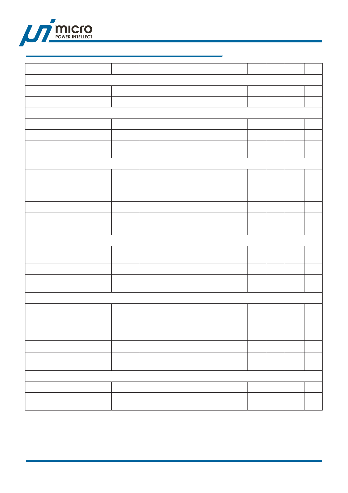
Electrical Characteristics
retemaraPlobmySsnoitidnoCtseTniMpyTxaMtinU
tratStfoS
tnerruCtratStfoSI
SS
leveLdlohserhTtratStfoS-eRV
V
PUCCIH_SS
V21=80121Au
CC
--5.0--V
noitceleSesahPnoitarepO
leveLdlohserhTgnisiREDOMV
leveLdlohserhTgnillaFEDOMV
V
EDOM
V
EDOM
emiThctilgeDniPEDOM
V21=4.1----V
CC
V21=----4.0V
CC
2lennahcothgih=EDOMmorF
delbasid
26 01su
rotallicsO
ycneuqerFgninnuReerFf
CSO
R
k33=072003033zHk
TR
noitairaVycneuqerF 01---01%
egnaRycneuqerF 05--0001zHk
elcyCytuDmumixaM 580959%
elcyCytuDmuminiM --0 --%
edutilpmApmaR ∆V
V
CSO
V21=--5.2--V
CC
egatloVecnerefeR
V
egatloVkcabdeeFlanimoNV
BF
CC
V,V21=
PMOC
V,V6.1=
V=
NIFER
,
5CC
egatlovecnereferV6.0lanretnignisu
195.06.0906.0V
P-P
egnaRNIFERV
tesffONIFERV
NIFER
V-
V|
NIFER
V,|
BF
CC
V5.2~4.0=
V,daoLoN,V21=
0--5.2V
NIFER
----01Vm
reifilpmArorrE
niaGCDpooLnepOOAngiseDybdeetnarauG0607--Bd
tcudorPhtdiwdnaB-niaGWBGngiseDybdeetnarauG601--zHM
etaRwelSRSngiseDybdeetnarauG36--su/V
ecnatcudnoc-snarTMGR
&ecruoS(tnerruCmumixaM
)kniS
I
PMOC
V
k02= Ω 00210071--V/Au
DAOL
V6.1=022082--Au
PMOC
esneStnerruC
tnerruCgnicroSmumixaMI
tesffOreifilpmAMGV
XAM_NSC
V
TESFFO
PSC
k02 Ω NSCmorfDNGot
RrotsiseratcennoC,V8.0=
=
NSC
001----Au
5-05 Vm
uPI Semiconductor Corp., http://www.upi-semi.com
Rev. 03, August 2007
12
Page 13
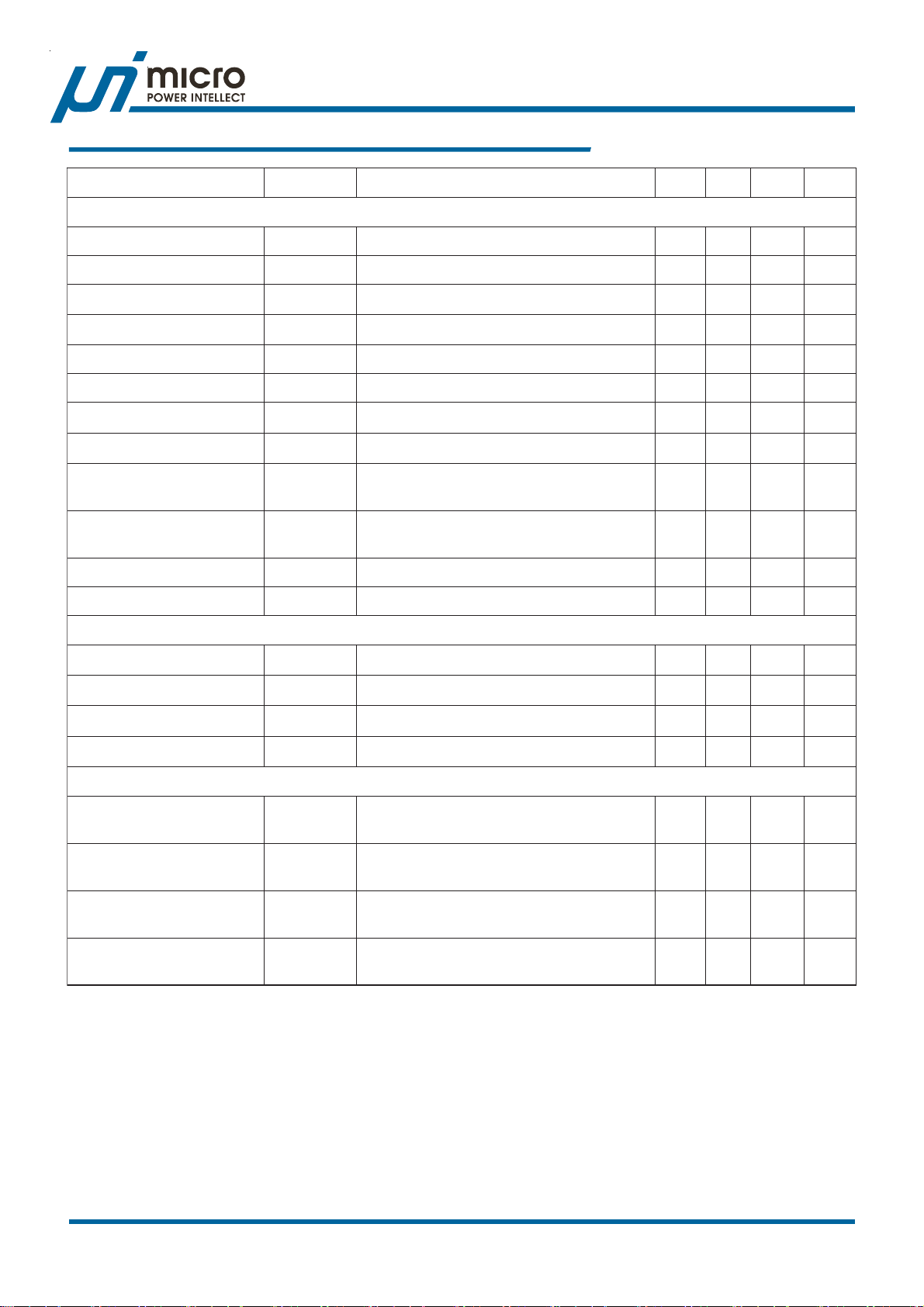
uP6201A/B
Electrical Characteristics
retemaraPlobmySsnoitidnoCtseTniMpyTxaMstinU
V(revirDetaG
CC
kniSetaGreppUI
kniSetaGreppUR
kniSetaGrewoLI
kniSetaGrewoLR
yaleDgnisiR
yaleDgnisiR
emiTdaeDT
)V21=
ecruoSetaGreppUI
ecruoSetaGreppUR
ecruoSetaGrewoLI
ecruoSetaGrewoLR
CRS_GU
KNS_GU
CRS_GU
KNS_GU
CRS_GL
KNS_GL
CRS_GL
KNS_GL
ETAGLotgnillaFESAHP
V
V
V
V
VCCV-
V
VCCV-
V
V
V-
TOOB
TOOB
TOOB
ETAGU
ETAGL
ETAGL
CC
ESAHP
V-
ESAHP
V-
ESAHP
V-
ETAGL
V6=--2 --A
ETAGL
V1=--24Ω
V;V21=
V2.1
ETAGUotgnillaFETAGL
V
CC
V
TD
V;V21=
ESAHP
emiTnOmuminiMgnitarepOcitatShtdiWesluP001051sn
V(revirDetaG
kniSetaGreppUR
kniSetaGrewoLR
)V9=
CC
ecruoSetaGreppUR
ecruoSetaGrewoLR
CRS_GU
KNS_GU
CRS_GL
KNS_GL
V
V
VCCV-
V
V-
TOOB
V-
ETAGU
ETAGL
ESAHP
ETAGL
V1=--2.24.4 Ω
noitcetorP
V,V21=
V,V21=
V,V21=
V1=--24Ω
ESAHP
V-
TOOB
V-
TOOB
V-
TOOB
V6=--5.1---A
ETAGU
V6=--2 --A
ETAGU
V1=--36Ω
ETAGU
V6=--5.1---A
V1=--36Ω
ESAHP
ETAGL
VotV2.1<
V2.1>)
>
ETAGL
V(otV2.1<
-
ETAGU
--03--sn
--03--sn
--03--sn
V,V9=
V1=--2.24.4 Ω
ESAHP
V-
TOOB
V1=--3.36.6 Ω
ETAGU
V1=--3.36.6 Ω
tnerruCrevOesahP
leveLnoitcetorP
tnerruCrevOlatoT
noitcetorP
I
PCO_NSC
I
PCO_MUS
erutarepmeTrevO
noitcetorP
erutarepmeTrevO
siseretsyH
I
I
Iro
1NSC
MUS
2NSC
I=
I+
1NSC
2NSC
--08--Au
--021--Au
--051--
--02--
O
O
Note 1. Stresses listed as the above “Absolute Maximum Ratings” may cause permanent damage to the device.
These are for stress ratings. Functional operation of the device at these or any other conditions beyond those
indicated in the operational sections of the specifications is not implied. Exposure to absolute maximum
rating conditions for extended periods may remain possibility to affect device reliability.
Note 2. Devices are ESD sensitive. Handling precaution recommended.
Note 3. θ
is measured in the natural convection at T
JA
= 25°C on a low effective thermal conductivity test board of
A
JEDEC 51-3 thermal measurement standard.
Note 4. The device is not guaranteed to function outside its operating conditions.
uPI Semiconductor Corp., http://www.upi-semi.com
Rev. 03, August 2007
C
C
13
Page 14
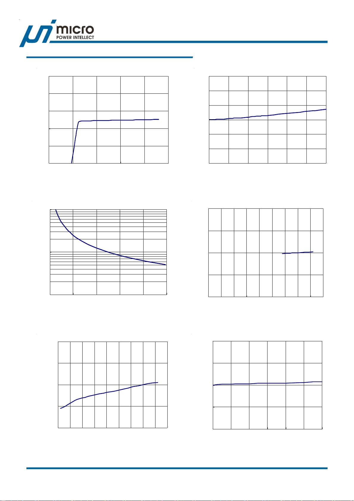
uP6201A/B
Typical Operation Characteristics
VCC5 Line Regulation
5.5
5.3
5.1
4.9
VCC5 (V)
4.7
4.5
4 6 8 10 12 14
VCC (V)
Switching Frequency vs. R
1000
VCC5 Load Regulation
5.15
5.1
5.05
5
VCC5 (V)
4.95
4.9
4.85
0 102030405060
VCC5 Load Current (mA)
RT
Output Voltage Line Regulation (VCC = 9V)
0.61
(V)
0.605
FB
100
Switching Frequency (kHz)
10
0 40 80 120 160 200
R
(kΩ)
RT
Output Voltage Line Regulation (VCC = VIN)
0.61
(V)
0.605
FB
0.6
0.595
Feedback Voltage V
0.6
0.595
Feedback Voltage V
0.59
567891011121314
Input Voltage V
(V)
IN
Output Voltage Load Regulation
0.61
(V)
0.605
FB
0.6
0.595
Feedback Voltage V
0.59
5 6 7 8 9 1011121314
Input Voltage VCC = V
uPI Semiconductor Corp., http://www.upi-semi.com
Rev. 03, August 2007
(V)
IN
0.59
0 102030405060
Output Current (A)
14
Page 15
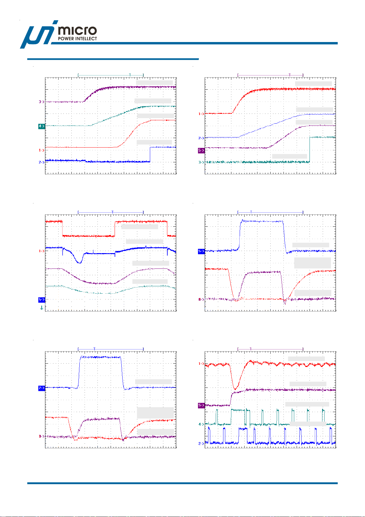
uP6201A/B
Typical Operation Characteristics
Power On
VIN (10V /Div)
SS (1V/Div)
V
(0.5V/Div)
OUT
POK (1V/Div)
Time (5ms/Div)
Reference Input Step Change
REFIN (0.5V/Div)
COMP (0.5V/Div)
Turn On by REFIN
REFIN (0.5V/Div)
SS (1V/Div)
V
(1V/Div)
OUT
POK (1V/Div)
Time (5ms/Div)
Switching Waveforms (VCC = 12V)
PHASE (5V/Div)
V
(1V/Div)
OUT
SS (1V/Div)
Time (250us/Div)
I
= 5A
OUT
Switching Waveforms (VCC = 9V)
PHASE (5V/Div)
UGATE - PHASE
(5V/Div)
LGATE (5V/Div)
UGATE - PHASE
(5V/Div)
LGATE (5V/Div)
Time (100ns/Div)
VCC = 12V, 20MHz bandwidth limited
Load Transient Response
V
(0.1V/Div)
OUT
I
(30A/Div)
OUT
Phase1 (10V/Div)
Phase 2 (1V/Div)
Time (100ns/Div)
VCC = 8V, 20MHz bandwidth limited
uPI Semiconductor Corp., http://www.upi-semi.com
Rev. 03, August 2007
Time (2.5us/Div)
I
= 0A to 40A
OUT
15
Page 16
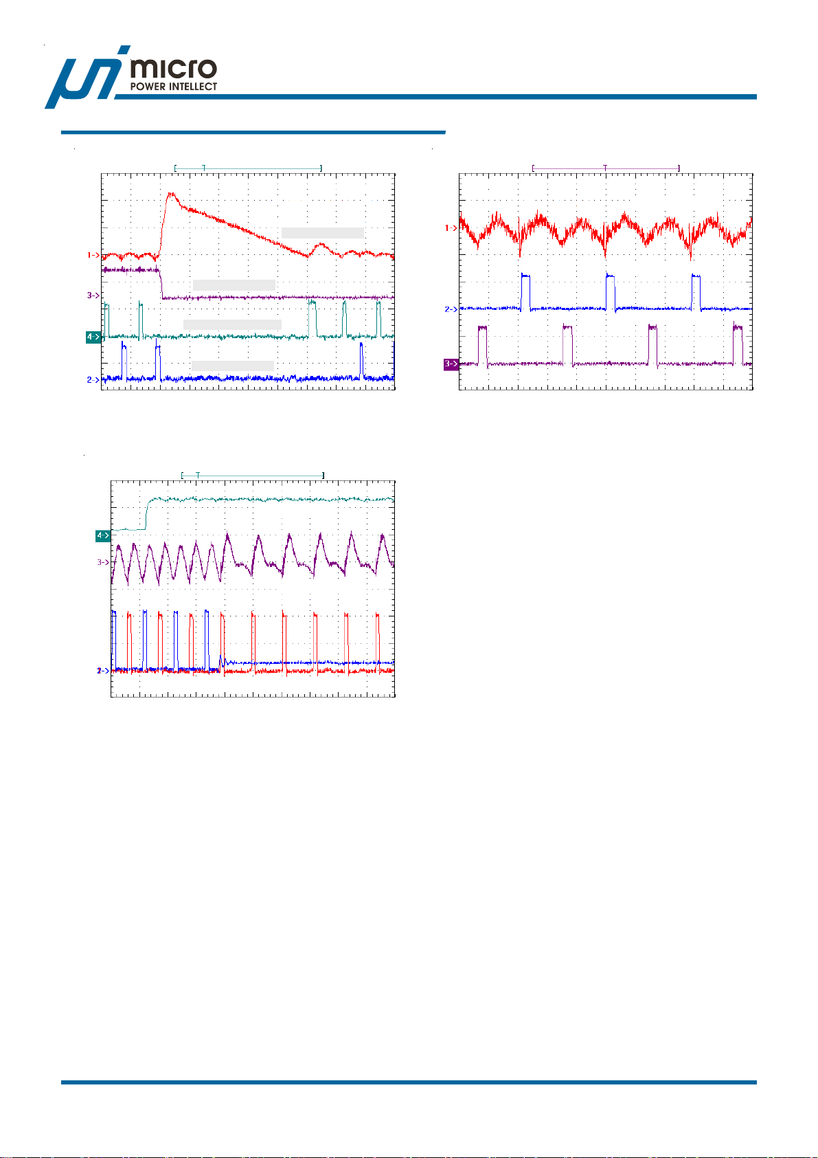
uP6201A/B
Typical Operation Characteristics
Load Transient Response
V
(0.1V/Div)
OUT
I
(30A/Div)
OUT
Phase1 (10V/Div)
Phase 2 (1V/Div)
Time 2.5s/Div
I
= 40A to 0A
OUT
Two To Single Phase Operation
MODE (2V/Div)
Steady State Operation
V
(20mV/Div)
OUT
PHASE1 (10V/Div)
PHASE2 (10V/Div
Time (1us/Div)
VIN = 12V, V
OUT
= 1.2V
Phase1 (10V/Div)
Time 2.5us/Div
V
(20mV/Div)
OUT
Phase 2 (10V/Div)
uPI Semiconductor Corp., http://www.upi-semi.com
Rev. 03, August 2007
16
Page 17

uP6201A/B
A
C
pplication Information
Component Selection Guidelines
The selection of external component is primarily determined
by the maximum load current and begins with the selection
of power MOSFET switches. The desired amount of ripple
current and operating frequency largely determines the
inductor value. Finally, CIN is selected for its capability to
handle the large RMS current into the converter and C
OUT
is chosen with low enough ESR to meet the output voltage
ripple and transient specification.
Power MOSFET Selection
The uP6201A/B requires two external N-channel power
MOSFETs for upper (controlled) and lower (synchronous)
switches. Important parameters for the power MOSFETs
are the breakdown voltage V
reverse transfer capacitance C
, on-resistance R
(BR)DSS
, maximum current I
RSS
DS(ON)
DS(MAX)
gate supply requirements, and thermal management
requirements.
The gate drive voltage is supplied by VCC pin that receives
4.5V~13.2V supply voltage. When operating with a 7~13.2V
power supply for VCC, a wide variety of NMOSFETs can
be used. Logic-level threshold MOSFET should be used if
the input voltage is expected to drop below 7V. Caution
should be exercised with devices exhibiting very low V
GS(ON)
characteristics. The shoot-through protection present
aboard the uP6201A/B may be circumvented by these
MOSFETs if they have large parasitic impedances and/or
capacitances that would inhibit the gate of the MOSFET
from being discharged below its threshold level before the
complementary MOSFET is turned on. Also avoid
MOSFETs with excessive switching times; the circuitry is
expecting transitions to occur in under 40ns or so.
In high-current applications, the MOSFET power
dissipation, package selection and heatsink are the
dominant design factors. The power dissipation includes
two loss components; conduction loss and switching loss.
The conduction losses are the largest component of power
dissipation for both the upper and the lower MOSFETs.
These losses are distributed between the two MOSFETs
according to duty cycle. Since the uP6201A/B is operating
in continuous conduction mode, the duty cycles for the
MOSFETs are:
D =
UP
V
OUT
V
;
IN
LOW
=
VVD−
OUTIN
V
IN
The resulting power dissipation in the MOSFETs at
maximum output current are:
2
OUTUP
2
OUTLOW
DRIP ××=
LOW)ON(DS
fTVI5.0DRIP ××××+××=
OSCSWINOUTUP)ON(DS
Both MOSFETs have I2R losses and the upper MOSFET
includes an additional term for switching losses, which are
largest at high input voltages. The lower MOSFET losses
are greatest when the bottom duty cycle is near 100%,
during a short-circuit or at high input voltage. These
equations assume linear voltage current transitions and do
not adequately model power loss due the reverse-recovery
of the lower MOSFET’s body diode.
Ensure that both MOSFETs are within their maximum
junction temperature at high ambient temperature by
calculating the temperature rise according to package
thermal-resistance specifications. A separate heatsink may
be necessary depending upon MOSFET power, package
type, ambient temperature and air flow.
,
The gate-charge losses are mainly dissipated by the
,
uP6201A/B and don’t heat the MOSFETs. However, large
gate charge increases the switching interval, TSW that
increases the MOSFET switching losses. The gate-charge
losses are calculated as:
UP_RSSINLO_ISSUP_ISSCCCCC_G
where C
C
ISS_LOW
C
RSS_UP
is the input capacitance of the upper MOSFET,
ISS_UP
is the input capacitance of the lower MOSFET, and
is the reverse transfer capacitance of the upper
MOSFET. Make sure that the gate-charge loss will not
cause over temperature at uP6201A/B, especially with
large gate capacitance and high supply voltage.
Output Inductor Selection
Output inductor selection usually is based on the
considerations of inductance, rated current, size
requirements and DC resistance (DCR).
Given the desired input and output voltages, the inductor
value and operating frequency determine the ripple current:
I
=∆
L
1
Lf
×
OUT
OUTOSC
V
OUT
1(V
−
)
V
IN
Lower ripple current reduces core losses in the inductor,
ESR losses in the output capacitors and output voltage
ripple. Highest efficiency operation is obtained at low
frequency with small ripple current. However, achieving this
requires a large inductor. There is a tradeoff between
component size, efficiency and operating frequency. A
reasonable starting point is to choose a ripple current that
is about 20% of I
OUT(MAX)
.
There is another tradeoff between output ripple current/
voltage and response time to a transient load. Increasing
the value of inductance reduces the output ripple current
and voltage. However, the large inductance values reduce
the converter’s response time to a load transient.
f)CV)CC(V(VP ××++××=
OS
where TSW is the combined switch ON and OFF time.
uPI Semiconductor Corp., http://www.upi-semi.com
Rev. 03, August 2007
17
Page 18

uP6201A/B
A
pplication Information
Maximum current ratings of the inductor are generally
specified in two methods: permissible DC current and
saturation current. Permissible DC current is the allowable
DC current that causes 40OC temperature raise. The
saturation current is the allowable current that causes 10%
inductance loss. Make sure that the inductor will not
saturate over the operation conditions including temperature
range, input voltage range, and maximum output current.
The size requirements refer to the area and height
requirement for a particular design. For better efficiency,
choose a low DC resistance inductor. DCR is usually
inversely proportional to size.
Input Capacitor Selection
The synchronous-rectified Buck converter draws pulsed
current with sharp edges from the input capacitor, resulting
in ripples and spikes at the input supply voltage. Use a
mix of input bypass capacitors to control the voltage
overshoot across the MOSFETs. Use small ceramic
capacitors for high frequency decoupling and bulk capacitors
to supply the current needed each time upper MOSFET
turns on. Place the small ceramic capacitors physically
close to the MOSFETs to avoid the stray inductance along
the connection trace.
The important parameters for the bulk input capacitor are
the voltage rating and the RMS current rating. For reliable
operation, select the bulk capacitor with voltage and current
ratings above the maximum input voltage and largest RMS
current required by the circuit. The capacitor voltage rating
should be at least 1.25 times greater than the maximum
input voltage and a voltage rating of 1.5 times is a
conservative guideline. The RMS current rating requirement
for the input capacitor of a buck converter is calculated as:
OUTINOUT
)VV(V
, where I
OUT
IN(REMS)
II
=
)MAX(OUT)RMS(IN
−
V
IN
This formula has a maximum at VIN = 2V
= I
/2. This simple worst-case condition is commonly
OUT(RMS)
used for design because even significant deviations do not
offer much relief. Note that the capacitor manufacturer’s
ripple current ratings are often based on 2000 hours of life.
This makes it advisable to further derate the capacitor, or
choose a capacitor rated at a higher temperature than
required. Always consult the manufacturer if there is any
question.
For a through-hole design, several electrolytic capacitors
may be needed. For surface mount designs, solid tantalum
capacitors can also be used, but caution must be exercised
with regard to the capacitor surge current rating. These
capacitors must be capable of handling the surge-current
at power-up. Some capacitor series available from reputable
manufacturers are surge current tested.
Output Capacitor Selection
The selection of C
is primarily determined by the ESR
OUT
required to minimize voltage ripple and load step transients.
The equivalent ripple current into the output capacitor is
half of the inductor ripple current while the equivalent
frequency is double of phase operation frequency due to
two phase operation The output ripple ∆V
OUT
is
approximately bounded by:
OUT
V
Since ∆I
∆
I
=∆
2
increases with input voltage, the output ripple is
L
+
ESR(
1
××
)
OUTOSC
Cf16
L
highest at maximum input voltage. Typically, once the ESR
requirement is satisfied, the capacitance is adequate for
filtering and has the necessary RMS current rating. Multiple
capacitors placed in parallel may be needed to meet the
ESR and RMS current handling requirements.
The load transient requirements are a function of the slew
rate (di/dt) and the magnitude of the transient load current.
These requirements are generally met with a mix of
capacitors and careful layout. Modern components and
loads are capable of producing transient load rates above
1A/ns. High frequency capacitors initially supply the
transient and slow the current load rate seen by the bulk
capacitors. The bulk filter capacitor values are generally
determined by the ESR (Effective Series Resistance) and
voltage rating requirements rather than actual capacitance
requirements.
High frequency decoupling capacitors should be placed as
close to the power pins of the load as physically possible.
Be careful not to add inductance in the circuit board wiring
that could cancel the usefulness of these low inductance
components. Consult with the manufacturer of the load on
specific decoupling requirements.
Use only specialized low-ESR capacitors intended for
switching-regulator applications for the bulk capacitors. The
bulk capacitor’s ESR will determine the output ripple voltage
and the initial voltage drop after a high slew-rate transient.
An aluminum electrolytic capacitor’s ESR value is related
to the case size with lower ESR available in larger case
sizes.
Bootstrap Capacitor Selection
An external bootstrap capacitor C
connected to the
BOOT
BOOT pin supplies the gate drive voltage for the upper
MOSFET. This capacitor is charged through the internal
diode when the PHASE node is low. When the upper
uPI Semiconductor Corp., http://www.upi-semi.com
Rev. 03, August 2007
18
Page 19
uP6201A/B
A
pplication Information
MOSFET turns on, the PHASE node rises to V
and the
IN
BOOT pin rises to approximately VIN + VCC. The boot
capacitor needs to store about 100 times the gate charge
required by the upper MOSFET. In most applications 0.47µF
to 1µF, X5R or X7R dielectric capacitor is adequate.
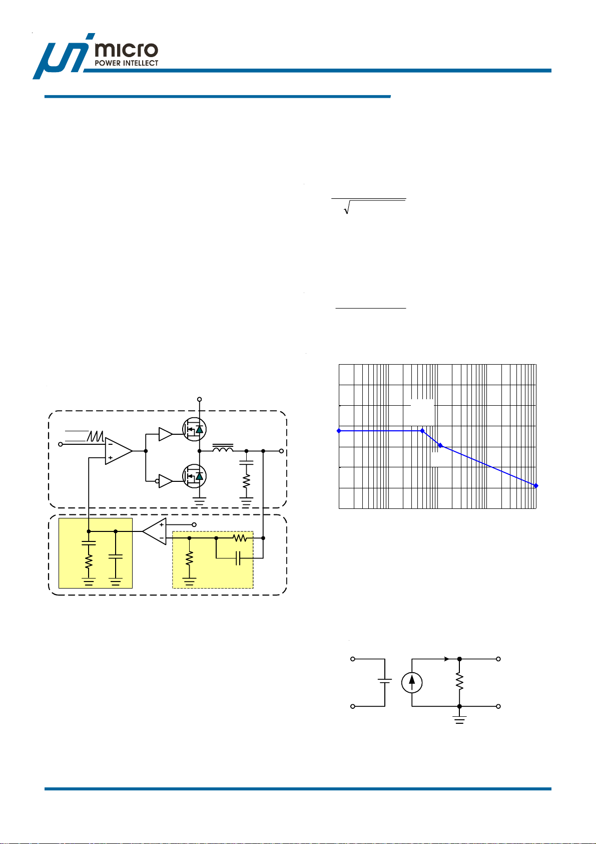
Feedback Loop Compensation
Figure 11 highlights the voltage-mode control loop for a
synchronous-rectified buck converter consisting of
uP6201A/B. The control loop includes a compensator and
a modulator, where the modulator consists of the PWM
comparator, the power stage amplifier and the output filter;
the compensator consists of the error amplifier and
compensating network. A well-designed feedback loop
tightly regulates the output voltage (V
voltage V
with fast response to load/line transient and
REF
) to the reference
OUT
good stability. The goal of the compensation network is to
provide and the highest 0dB crossing frequency and
adequate phase margin (greater than 45 degrees). It is also
recommended to manipulate loop frequency response that
its gain crosses over 0dB at a slope of -20dB/dec.
V
IN
∪V
OSC
Driver
PHASE
PWM
Comp.
L
OUT
C
OUT
ESR
Modulator
V
OUT
voltage £GV
OSC
.
The output LC filter introduces a double pole, 40dB/decade
gain slope above its corner resonant frequency, and a total
phase lag of 180 degrees. The resonant frequency of the
LC filter expressed as:
F×π=
LC
1
CL2
OUTOUT
The ESR zero is contributed by the ESR associated with
the output capacitor. Note that this requires that the output
capacitor should have enough ESR to satisfy stability
requirements as described in the later sections. The ESR
zero of the output capacitor expressed as:
F
ESR
=
1
CESR2
××π
OUT
Figure 12 illustrates frequency response of a typical
modulator using uP6201A/B.
80
60
40
20
0
Gain (dB)
-20
-40
LC
Doubl e
Pole
ESR
Zero
V
REF
R2
Compensator
R3
C3
Z
FB
Z
C1
COMP
R1
V
COMP
Error
Amp.
C2
Figure 10. Voltage-Mode Control Loop of uP6201A/B.
Modulator Break Frequency Equations
The error amplifier output (V
) is compared with the
COMP
oscillator (OSC) sawtooth waveform to provide a pulse-width
modulated (PWM) waveform with an amplitude of VIN at the
PHASE node. The PWM waveform is smoothed by the
output filter (L
is the small-signal transfer function of V
OUT
and C
). The modulator transfer function
OUT
OUT/VCOMP
. This
function is dominated by a DC Gain and the output filter
(L
and C
OUT
and a zero at F
), with a double pole break frequency at F
OUT
. The DC Gain of the modulator is simply
ESR
the input voltage (VIN) divided by the peak-to-peak oscillator
uPI Semiconductor Corp., http://www.upi-semi.com
Rev. 03, August 2007
-60
1.E+02 1.E+03 1.E+04 1.E+05 1.E+06
Frequency (Hz)
Figure 12. Frequency Response of Modulator.
2) Compensator Frequency Equations
The uP6201A/B adopts an operational transconductance
amplifier (OTA) as the error amplifier as shown in Figure
13.
EA+
∆V
OUT
M
GM
M
V
OUT
R
OUT
∆I
= GM x ∆V
EA-
LC
Figure 13. Operational Transconductance Amplifier.
The transconductance is defined as:
19
Page 20
uP6201A/B
A
pplication Information
I
∆
GM
∆VM = (EA+) - (EA-); ∆I
OUT
=
V
∆
M
= E/A output current.
OUT
Figure 14 illustrates a type II compensation network using
OTA. The compensation network consists of the error
amplifier and the impedance networks ZFB and Z
V
OUT
R3
Z
FB
R2
GM
Error
Amplifier
C2
V
REF
Z
COMP
V
COMP
COMP
R1
C1
.
Figure 14. Type II Compensation Network Using OTA.
The compensator transfer function is the small-signal
transfer function of V
COMP/VOUT
by a Mid-Band Gain and compensation network Z
. This function is dominated
, with
COMP
a pole at FP1 and a zero at FZ1. The Mid-Band Gain of the
compensation is expressed as:
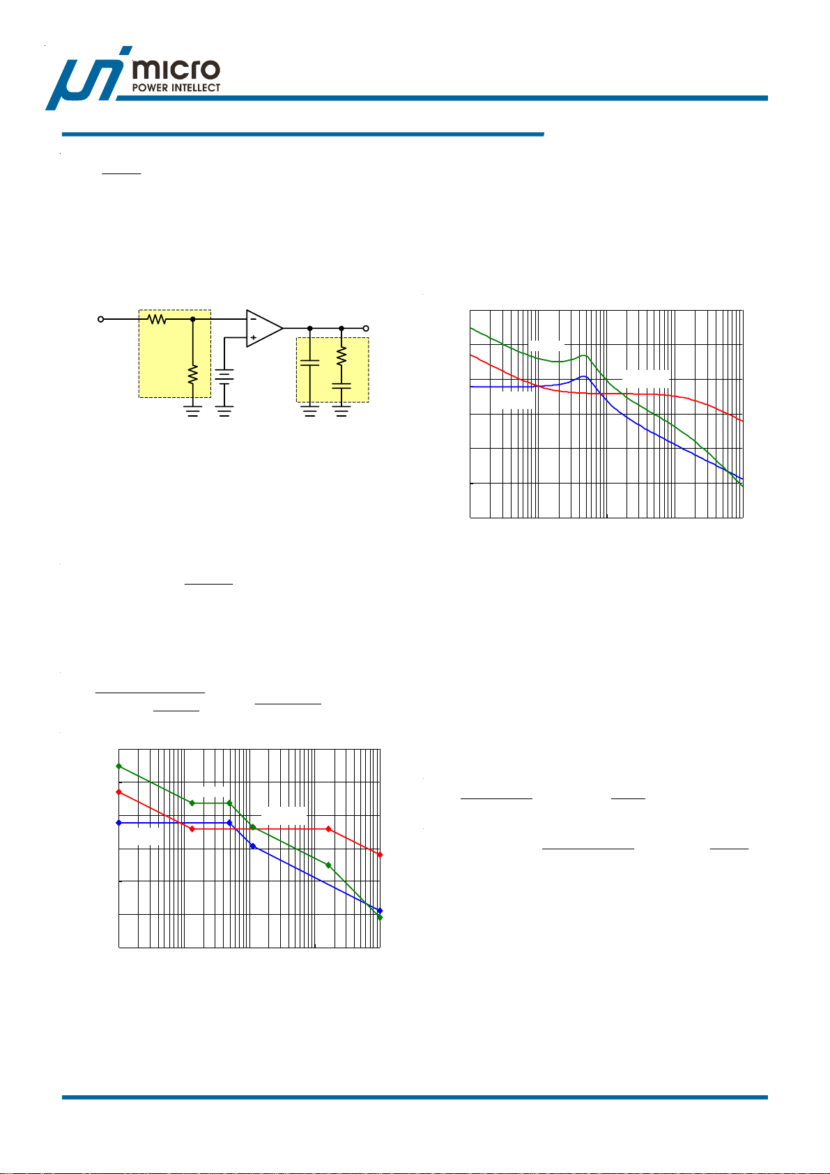
and fast response to load/line transient with good stability.
Follow the guidelines for locating the poles and zeros of
the compensation network.
1. Pick Mid-Band Gain (R1) for desired converter bandwidth.
2. Place Zero (C1) below LC double pole (~20% PLC).
3. Place Pole (C2) at half the switching frequency.
4. Check gain against error amplifier open loop gain.
5. Estimate phase margin - repeat if necessary.
60
40
20
0
Gain (dB)
-20
-40
-60
1.E+02 1.E+03 1.E+04 1.E+05 1.E+06
Modulator
Gain
Loop Gain
Compensator
Frequency (Hz)
Gain
Gain_Band_Mid ××
2R
=
3R2R
×
GM1R
The equations below relate the compensation network’s
pole and zero to the components (R1, C1, and C2) in Figure
15.
F
=
1P
60
40
20
R1
C1
0
Gain (dB)
-20
-40
-60
1.E+02 1.E+03 1.E+04 1.E+05 1.E+06
1
(1R2
××π
Modulator
Gain
×
+
2C1C
;
)
2C1C
Loop Gain
F
Z1
Frequency (Hz)
=
1
××π
Compensat or
Gain
1C1R2
F
P1
F
1Z
Figure 15. Frequency Response of Type II Compensation.
Figure 16 shows the DC-DC converter’s gain vs. frequency.
Careful design of Z
COMP
and Z
provides tight regulation
FB
Figure16. Frequency Response of Type II Compensation.
Design Example
As a design example, take a power supply with the following
specifications:
VIN = 10.8V to 13.2V (12V nominal), V
I
OUT(MAX)
= 40A, f
= 300kHz, ∆V
OSC
= 20mV, bandwidth =
OUT
= 1.2V ¡Ó5%,
OUT
60kHz.
1.) Power Component Selection
First, choose the inductor for about 20% ripple current at
the maximum VIN:
I
L
L
OUT
=∆
1
Lf
×
OUTOSC
uH 45.0L
=
OUT
%20A40I
=×=∆
V
OUT
V
OUT
)
IN
V2.1
1(V2.1
−××
)
V2.13
1(V
−××
1
LkHz300
×
Selecting a standard value of 0.47uH results in a maximum
ripple current of 7.7A. The ripple current into output
capacitors is 3.9A.
Choose two 1000uF capacitors with 10mΩ ESR in parallel
to yield equivalent ESR = 5mΩ. The output ripple voltage
is about 20mV accordingly. An optional 22uF ceramic output
capacitor is recommended to minimize the effect of ESL in
the output ripple.
The modulator DC gain and break frequencies are calculated
uPI Semiconductor Corp., http://www.upi-semi.com
Rev. 03, August 2007
20
Page 21
uP6201A/B
A
pplication Information
as:
F
F
LC
ESR
V
log(20Gain DC
×=
=
=
IN
V
∆
OSC
1
1020001047.02
×××π
1
−−
1020001052
××××π
12
log(20)
5.2
kHz2.5
=
66
−−
kHz16
=
63
dB6.13)
=×=
2.) Compensation
Select R2 = R3 = 10kΩ to set output voltage as 1.2V. R2
and R3 do not affect the compensation, 1kΩ ~ 10kΩ is
adequate for the application.
The modulator gain at zero-crossing frequency (60kHz) is
calculated as -17.4dB. This demands a compensator with
mid-band gain as 17.4dB. Select R1 as:
)20/4.17(
×
V10
= k7.8
1R
OUT
×
VGM
REF
Select C1 = 13nF to place F
Ω=
= 1.4kHz, about one fifth of
Z1
the LC double pole.
Select C2 = 68pF to place FP1 = 270kHz, about half of the
equivalent switching frequency.
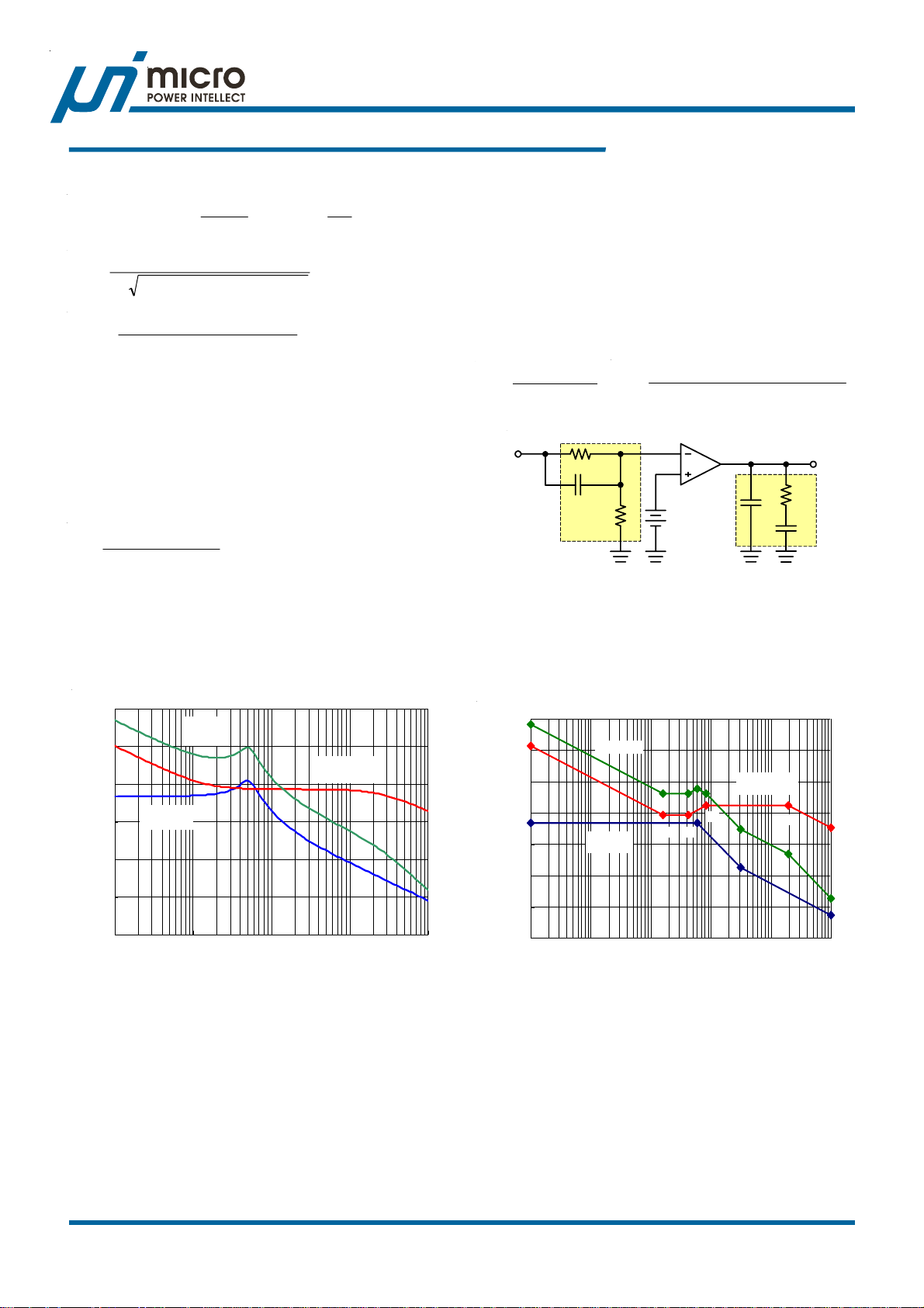
Figure 17 shows the result loop gain vs. frequency relation.
Type III Compensation
A type III compensation network as shown in Figure 18
that features 2 poles and 2 zeros is necessary for such
applications where ESR zero is far away from the LC double
pole. Adding a feedforward capacitor C3 on original type II
compensation network introduces an additional pole-zero
pair ( Z2 and P2) as illustrated in Figure 19. The new polezero pair are expressed as:
Error
1
+×××π
)3R2R/()3R2R(3C2
V
COMP
R1
C2
Z
C1
COMP
2Z
=
1
××π
V
OUT
Z
2P
=
;
3C3R2
R3
C3
FB
R2
GM
Amplifier
V
REF
Figure 19. Type III Compensation Network.
While the Mid-Band Gain remains unchanged, the additional
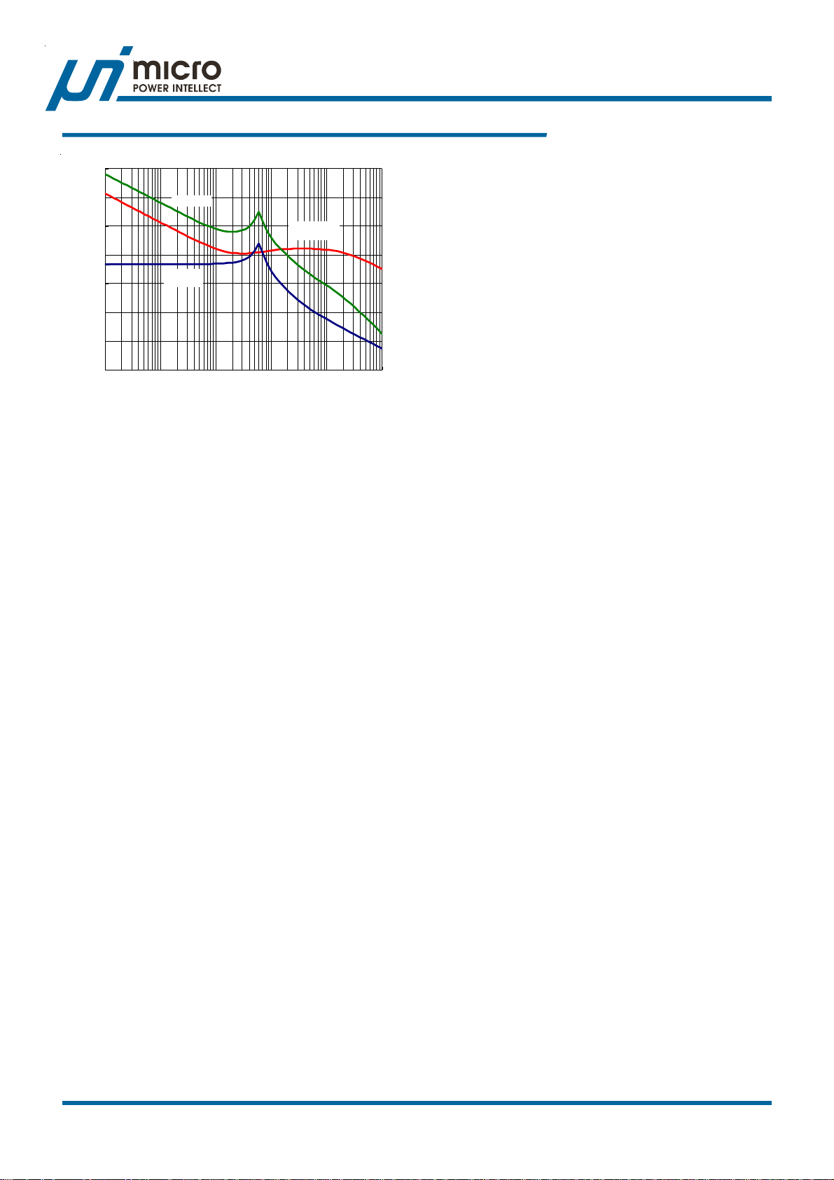
pole-zero pair causes a gain boost at the flat gain region.
The gain-boost is limited by the ratio (R1 +R2)/R2. Figures
20 and 21 show the DC-DC converter’s gain vs. frequency.
60
40
20
Modu lator
0
Gain (dB)
-20
-40
-60
1.E +02 1.E+03 1.E+ 04 1. E+05 1. E+06
Loop
Gai n
Compensato r
Gai n
Gai n
Frequenc y (Hz)
Figure 17. Gain vs. Frequency for the Design Example.
The ESR zero plays an important role in type II
compensation. Output capacitors with low ESR and small
capacitance push the ESR zero to high frequency band. If
the ESR zero is ten times higher than the LC double pole,
the double pole may cause the loop phase close to 180
and make the control loop unstable. A type II compensation
cannot stabilize the loop since it has only one zero.
80
Loop Gain
Modulator
Gain
Compensator
Gain
P2
Z1 Z2
Gain (dB)
60
40
20
0
-20
-40
-60
1.E+01 1.E+02 1.E+03 1.E+04 1.E+05 1.E+06
Frequency (Hz)
Figure 20. Loop Gain of Type III Compensation Network.
O
P1
uPI Semiconductor Corp., http://www.upi-semi.com
Rev. 03, August 2007
21
Page 22
uP6201A/B
A
pplication Information
80
60
40
20
0
Gain (dB)
-20
-40
-60
1.E+01 1.E+02 1.E+03 1.E+04 1.E+05 1.E+06
Loop Gain
Modulator
Gain
Frequency (Hz)
Compensator
Gain
Figure 21. Frequency Response of Type III Compensation.
Checking Transient Response
The regulator loop response can be checked by looking at
the load transient response. Switching regulators take
several cycles to respond to a step in load current. When
a load step occurs, V
equal to ∆I
resistance of C
C
generating a feedback error signal used by the
OUT
x(ESR), where ESR is the effective series
LOAD
. ∆I
OUT
regulator to return V
During this recovery time, V
immediately shifts by an amount
OUT
also begins to charge or discharge
LOAD
to its steady-state value.
OUT
can be monitored for
OUT
overshoot or ringing that would indicate a stability problem.
PCB Layout Considerations
High speed switching and relatively large peak currents in
a synchronous-rectified buck converter make the PCB layout
a very important part of design. Fast current switching from
one device to another in a synchronous-rectified buck
converter causes voltage spikes across the interconnecting
impedances and parasitic circuit elements. The voltage
spikes can degrade efficiency and radiate noise that result
in overvoltage stress on devices. Careful component
placement layout and printed circuit board design minimizes
the voltage spikes induced in the converter.
Follow the layout guidelines for optimal performance of
uP6201A/B.
1 The upper and lower MOSFETs turn on/off and conduct
pulsed current alternatively with high slew rate transition.
Any inductance in the switched current path generates
a large voltage spike during the switching. The
interconnecting wires indicated by red heavy lines
conduct pulsed current with sharp transient and should
be part of a ground or power plane in a printed circuit
board to minimize the voltage spike. Make all the
connection the top layer with wide, copper filled areas.
2 Place the power components as physically close as
possible.
2.1 Place the input capacitors, especially the high
frequency ceramic decoupling capacitors, directly
to the drain of upper MOSFET ad the source of the
lower MOSFET. To reduce the ESR replace the
single input capacitor with two parallel units
2.2 Place the output capacitor between the converter
and load.
3 Place the uP6201A/B near the upper and lower MOSFETs
with UGATE and LGATE facing the power components.
Keep the components connected to noise sensitive pins
near the uP6201A/B and away from the inductor and
other noise sources.
4 Use a dedicated grounding plane and use vias to ground
all critical components to this layer. The ground plane
layer should not have any traces and should be as close
as possible to the layer with power MOSFETs. Use an
immediate via to connect the components to ground
plane including GND of uP6201A/B Use several bigger
vias for power components.
5 Apply another solid layer as a power plane and cut this
plane into smaller islands of common voltage levels. The
power plane should support the input power and output
power nodes to maintain good voltage filtering and to
keep power losses low. Also, for higher currents, it is
recommended to use a multilayer board to help with
heat sinking power components.
6 The PHASE node is subject to very high dV/dt voltages.
Stray capacitance between this island and the
surrounding circuitry tend to induce current spike and
capacitive noise coupling. Keep the sensitive circuit away
from the PHASE node and keep the PCB area small to
limit the capacitive coupling. However, the PCB area
should be kept moderate since it also acts as main heat
convection path of the lower MOSFET.
7 The uP6201A/B sources/sinks impulse current with 2A
peak to turn on/off the upper and lower MOSFETs. The
connecting trance between the controller and gate/
source of the MOSFET should be wide and short to
minimize the parasitic inductance along the traces.
8 Flood all unused areas on all layers with copper. Flooding
with copper will reduce the temperature rise of power
component.
9 Provide local VCC decoupling between VCC and GND
pins. Locate the capacitor, C
as close as possible
BOOT
to the BOOT and PHASE pins.
uPI Semiconductor Corp., http://www.upi-semi.com
Rev. 03, August 2007
22
Page 23
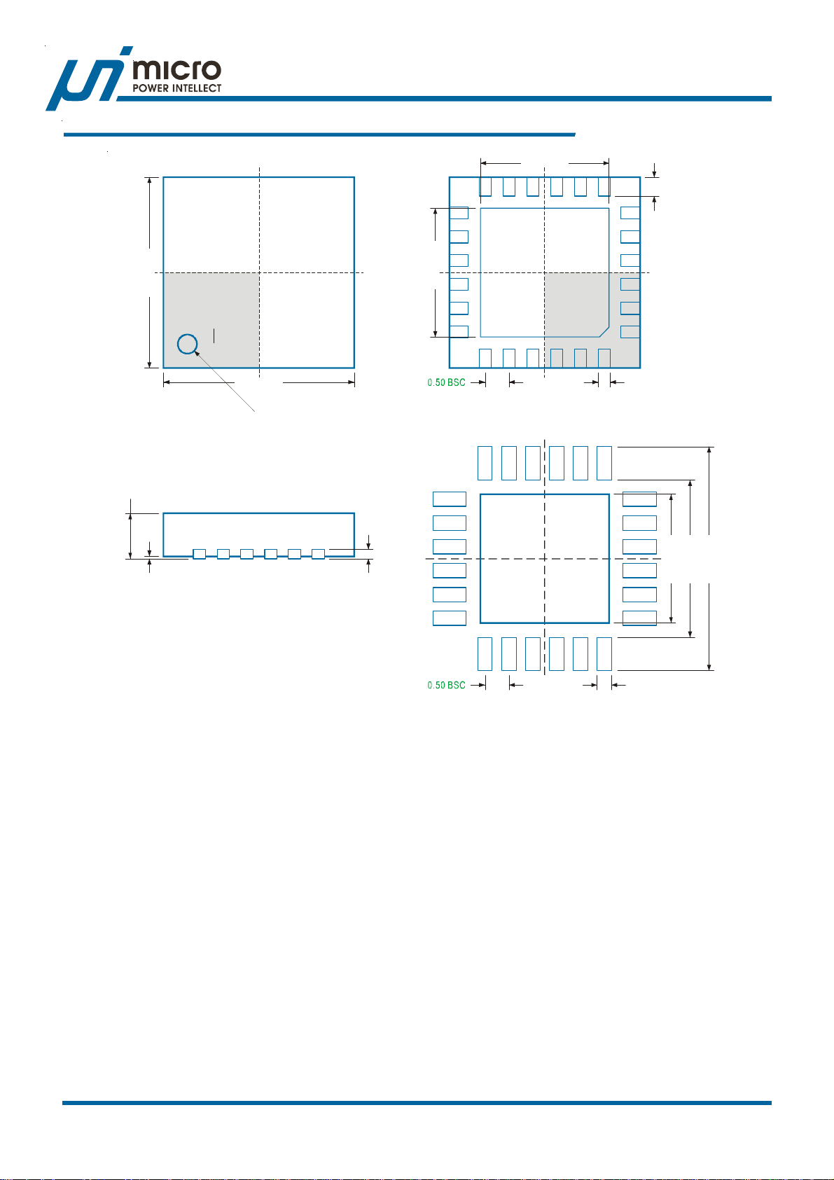
uP6201A/B
Package Information
0.80 - 1.00
2.30 - 2.75
3.90 - 4.10
3.90 - 4.10
2.30 - 2.75
0.35 - 0.45
0.18 - 0.30
Bottom View - Exposed Pad
Pin 1 mark
(Note 6)
2.65 - 2.75
3.10 - 3.20
4.50 - 4.70
0.0 - 0.05
0.20 BSC
0.20 - 0.30
Recommended Solder Pad Pitch and Dimensions
Note
1.Package Outline Unit Description:
BSC: Basic. Represents theoretical exact dimension or dimension target
MIN: Minimum dimension specified.
MAX: Maximum dimension specified.
REF: Reference. Represents dimension for reference use only. This value is not a device specification.
TYP. Typical. Provided as a general value. This value is not a device specification.
2.Dimensions in Millimeters.
3.Drawing not to scale.
4.These dimensions no not include mold flash or protrusions. Mold flash or protrusions shell not exceed 0.15mm.
uPI Semiconductor Corp., http://www.upi-semi.com
Rev. 03, August 2007
23
 Loading...