

Page 1
Preliminary
A
uP6161
Single 12V Input Supply Dual Regulator -
Synchronous-Buck-PWM and Line ar-Regulator Controller
General Description
The uP6161 integrates a high performa nce synchronousrectified buck controller a nd a linear-regulator controller.
This part works with a single +12V supply voltage and
delivers two high quality output voltages for both processing
unit and memory unit. An internal linear regulator provides
optimum 9V drive voltage for efficiency and thermal
man age ment.
The buck controller features internal MOSFET drivers that
supports bootstrapped voltage for high efficiency power
conversion. The bootstra p diode is built-in to si mplify the
circuit design and minimize external part count. It
incorporates simple, single feedba ck loop, voltage-control
with fast tra nsient response.
The linear controller drives a n external N-Cha nnel MOSFET
with under voltage protection during both soft start and
normal operation.
Other features include adjustable operation frequency,
internal soft start, under voltage protection, adjustable over
current protection and shutdown function. With the above
function, this part provides customers a compact, well
protected and cost-effe ctive solution. This part is available
in SOP-14 and QFN3x3 -16L pack ages.
pplications
Power Supplies for Microprocessors or
Subsystem Power Supplies
Cable Modems, Set Top Boxes, and DSL
Modems
Industrial Power Supplies; General Purpose
Supplies
12V Input DC-DC Regulators
Low-Voltage Distributed Power Supplies
Features
Operate with Single 12V Supply
Self-Regulated 9V Drive Voltage
Integrated Boot Diode
Provide Two Regulated Voltages
One Synchronous-Rectified Buck Controller
One Linear Controller
Both Controllers Drive N-Channel MOSFETs
Smaller Converter Size
Excellent Output Voltage Regulation
1.5% for Buck Controller
2% for Linear Controller
Simple Single-Loop Control Design
V oltage-Mode PWM Control
Fast T ran sient Respon se
High-Bandwidth Error Amplifier
Lossless, Progra mmable Overcurrent Protection
Uses Lower MOSFET R
Adjustable Frequency from 150kHz to 1MHz
Internal Soft Start for Both Outputs
Under V oltage Protection f or Both Outputs
including Soft Start Cycle
SOP-14 and QFN3x3-16 pa ckages
RoHS Compliant and 100% Lead Free
DS(ON)
Ordering Inf o rmation
rebmuNredrOepyTegakcaPkrameR
41S1616Pu41-POS
Q1616Pu61-3x3NFQ
Note: uPI products are compatible with the current IPC/
JEDEC J-STD-020 a nd RoHS requirements. They are 100%
matte tin (Sn) plating and suitable f or use in SnPb or Pbfree soldering processes.
uPI Semiconductor Corp., http://www.upi-semi.com
Rev. P00, File Name: uP6161-DS-P0001
1
Page 2
Preliminary
uP6161
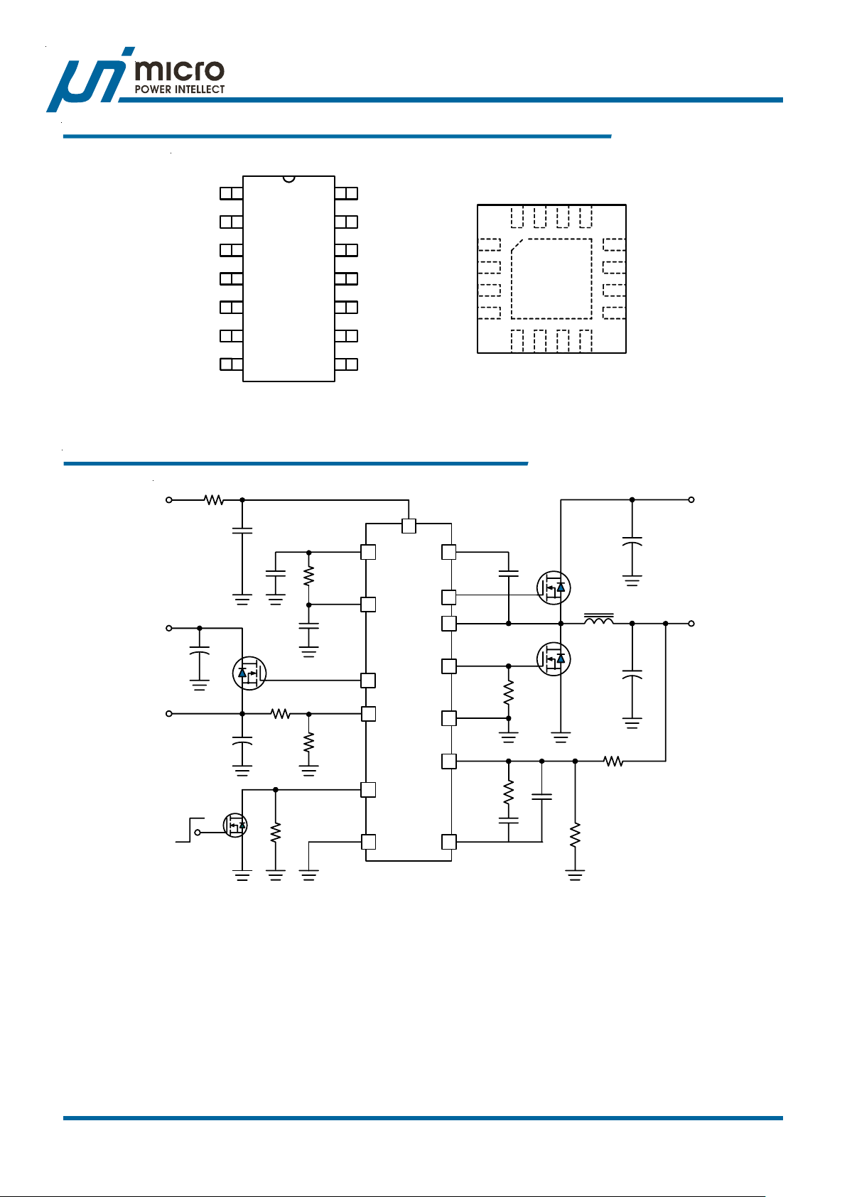
Pin Configuration
RT/DIS
COMP
FB
LDRV
LFB
AGND
+12V
V
IN2
1
2
3
14
13
12
411
5
10
6
78
UGATEBOOT
PHASE
PGND
LGATE
PVCC9
VCC9
9
VCC12
SOP-14
PVCC9
10
VCC9
9
8
COMP
LDRV
VCC12
LFB
1
14
13
FB
BOOT
UGATE
PHASE
RT/DIS
16
1
2
3
4
PGND
5
AGND
QFN3x3 – 16L
T ypical Applic ation Circui t
PHASE
UGATE
BOOTPGND
15
14
13
PGND
12
LGATE
11
PVCC9
10
VCC9
9
6
7
8
VCC12
VCC12
V
IN1
V
OUT1
V
Enable
OUT2
Disable
LDRV
LFB
RT/DIS#
GND
LGATE
11
5
6
2
7
uP6161S14
PGND
13
FB
4
3
COMP
R1
R2
uPI Semiconductor Corp., http://www.upi-semi.com
Rev. P00, File Name: uP6161-DS-P0001
2
Page 3
SS3
SS2
SS1
Soft
Start
Preliminary
POR &
Reference
VCC5
Internal
Regulator
uP6161
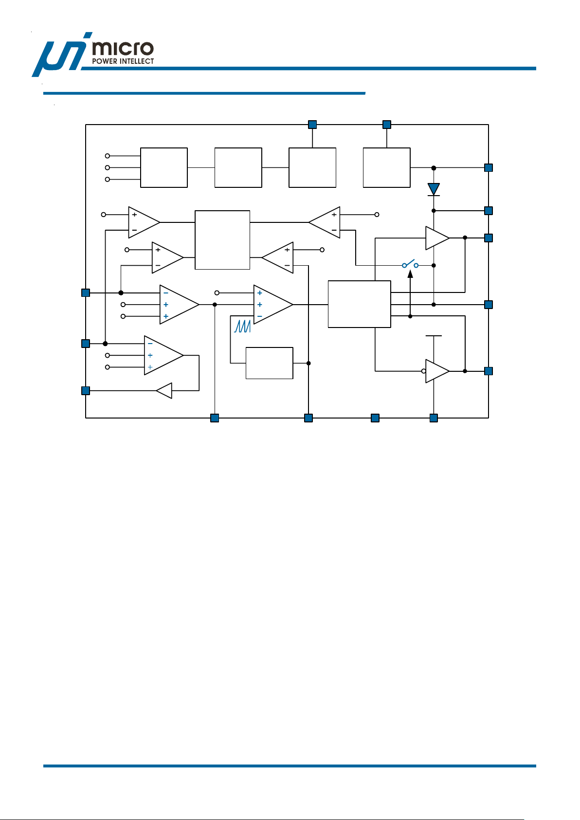
Functional Block Diagram
VCC12VCC9
Internal
Regulator
PVCC9
FB
LFB
LDRV
0.6V
0.8V
SS3
0.6V
0.8V
SS2
Enable &
Protection
Logic
SS1
Oscillator
0.4V
V
OCP
Gate
Control
Logic
BOOT
UGATE
PHASE
PVCC9
LGATE
PGNDGNDRT/DISCOMP
uPI Semiconductor Corp., http://www.upi-semi.com
Rev. P00, File Name: uP6161-DS-P0001
3
Page 4
Preliminary
n
uP6161
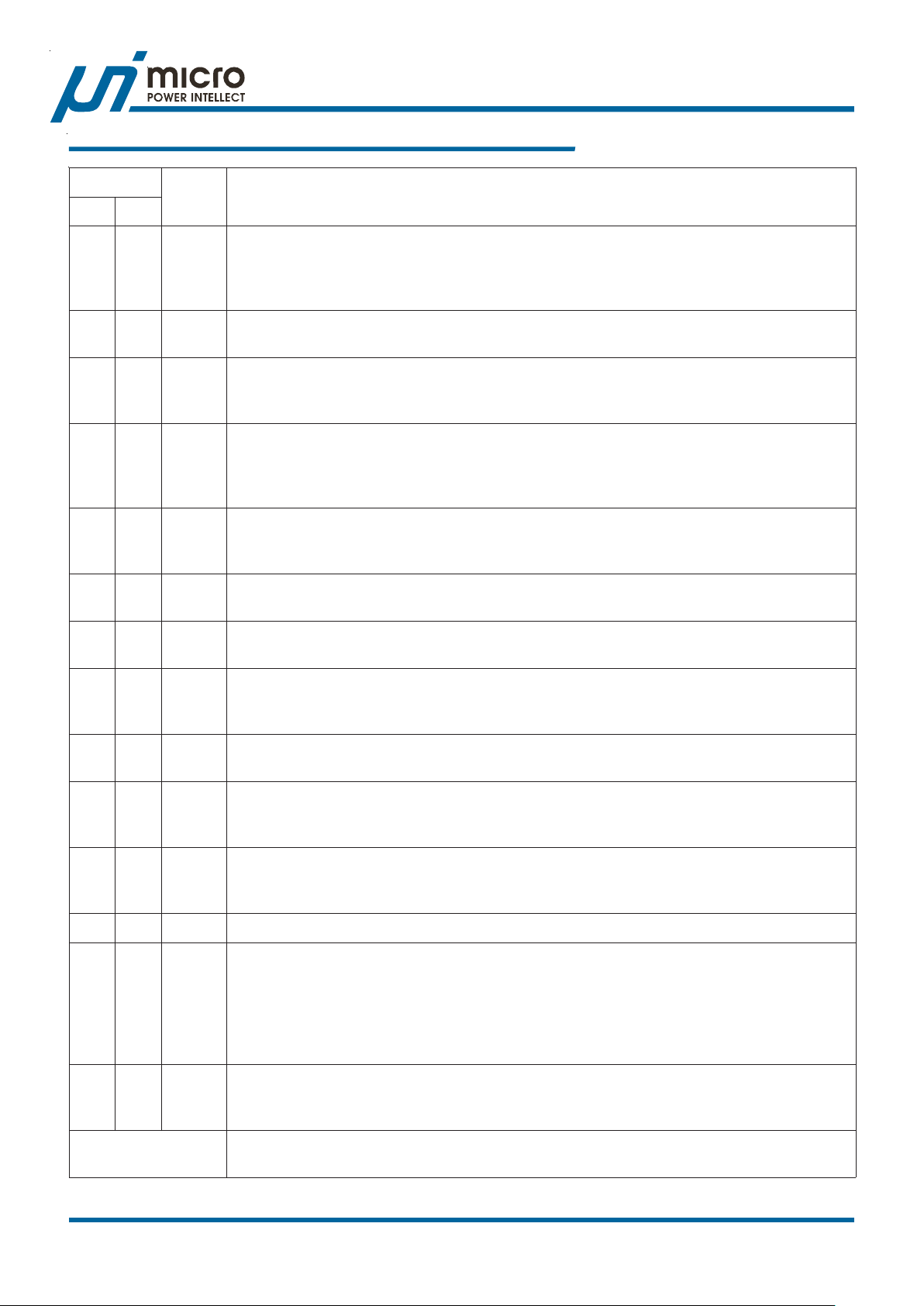
Function al Pin Descriptio
.oNniP
POSNFQ
151TOOB
261SID/TR
31 PMOC
42 BF
53 VRDL
64 BFL
niP
emaN
deeF .reifilpmarorreehtottupnignitrevniehtsinipsihT
noitcnuFniP
ylppuSpartstooB CroticapacpartstoobehttcennoC.revirdetagreppugnitaol
trevnoc
.re
.rotaluger
egatloVkcabdeeF .reifilpmarorreehtottupnignitrevniehtsinipsihT
fehtrof
ehtnonrutotegrahcehtsedivorpC
CtahterusnE.Fu74.0ot
TOOB
.elbasiDpihCdnagnitteSycneuqerF foycneuqerfnoitarepoehtstesDNGotrotsiserA
.tuptuOreifilpmArorrE gnitr
U.rotarapmocMWPehtfotupni
.retrevnoCkcuBrofegatloVkcab
ptuoehtmorfredividrotsiserA
.rotalugeRraeniLroftuptuOrevirD rotalugerraenilehtrofegatlovetagehtsedivorpnipsihT
.rotalugeRraeniLrof
tuoehtmorfredividrotsiserA
.CIehtraendecalpsi
.retrevnockcubehtfopoolkcabdeeflortnoc-egatlov
rofseulavlacipyT.TEFSOMreppu
TOOB
talugerraenildnakcubhtobselbasidDNGotnipsihtgnilluP.retrevnockcubehtrof
ofotTEFSOMlennahC-NlanretxenafoetagehtotnipsihttcennoC.rotsisnartssap
.egatlovnoitalugerehttesotdesusiDNGottup
TOOB
roticapacpartstoobehT.tiucricpartstoobamrofotnipESAHPehtdnanipTOOBneewteb
Fu1.0morfegnar
.sro
evni-nonehtdna)AE(reifilpmarorreehtfotuptuoehtsisihT
ehtetasnepmocotnipBFehthtiwnoitanibmocninipsihtes
ninipsihtesU.egatlovnoitalugerehttesotdesusiDNGottu
ehtfopoolkcabdeeflortnocegatlovehtetasnepmocotnipPMOCehthtiwnoitanibmoc
raenilamr
75 DNGA
88,721CCV
99 9CCV
01019CCVP
1111ETAGL
2121,6DNGP
3131ESAHP
4141ETAGU
lovllA
.CIehtrofdnuorGlangiS sihteiT.nipsihtottcepserhtiwderusaemeraslevelsegat
.egatloVylppuS rot
.egatlovtupnieht
.9CCV yllacisyhproticapaccimarecFu1muminimA.CI
woP deriuqertnerrucsedivorptI.rotalugerraenilV9lanretniehtfotuptuoehtsisihT
isyhp
.9CCVPre
.tuptuOrevirDetaGrewoL sinipsihT.TEFSOMrewolfoetagehtotnipsihttcennoC
.ffonrutsahTEFSOM
.CIehtrofdnuorGrewoP
.edoNhctiwSESAHP foniardehtdnaTEFSOMreppuehtfoecruosehtotnipsihttcennoC
wolehtssorcapordegatlov
csihcihwegatlovtneisnart
.tuptuOrevirDetaGreppU sinipsihT.TEFSOMreppufoetagehtotnipsihttcennoC
.ffodenrutsahTEFSOM
.elbaliavanoitcennocecnadepmitsewolehthguorhtenalp/dnalsidnuorgehtotnip
alugerV9lanretniehtsecruosti;CIehtrofnipylppusrewopehtsisihT
arecFu1muminimA.srevirdetagehtotdesu
ehtroftnerrucsaibseilppusnipsihT
.egatlovtupniehtgnissapybyllacolrofderiuqersiCIehtraen
.retrevnockcubfosTEFSOMlennahC-Ngnivirdrof
.egatlovtupniehtgnissapybyllacolrofderiuqersiCIehtraenyllac
otyrtiucricnoitcetorphguorht-toohsevitpadaehtybderotinom
AGUehtrofknisehtsadesusinipsihT.TEFSOMrewoleht
.metsysylppusrewopaninommo
gnissapybyllacolrofderiuqersiroticapaccim
roticapaccimarecFu1muminimA
rewolehtnehwenimreted
ehtrotinomotdna,revirdET
derotinomoslasinipsihT.noitcetorptnerrucrevorofTEFSOMre
sahTEFSOMreppuehtnehwenimretedotyrtiucricnoitcetorphguorht-toohsevitpadaehtyb
vitagenecuderotdednemmocersidnuorgdnanipsihtneewtebedoidykttohcSA.ffodenrut
e
ppuehtnehwenimretedotyrtiucricnoitcetorphguorht-toohsevitpadaehtybderotinom
re
pxE
uPI Semiconductor Corp., http://www.upi-semi.com
Rev. P00, File Name: uP6161-DS-P0001
daPdeso
.CIehtrofdnuorGrewoP deredlosllewebdluohsdapdesopxesihT.ylnoegakcapNFQroF
nnoC.noitcudnoctaehevitcefferofBCPot
.dnuorgehtdapdesopxeehttce
4
Page 5
Preliminary
)
uP6161
Functional Description
The uP6161 integrates a high performa nce synchronousrectified buck controller a nd a linear-regulator controller.
This part works with a single +12V supply voltage and
delivers two high quality output voltages for both processing
unit and memory unit. An internal linear regulator provides
optimum 9V drive voltage for efficiency and thermal
man age ment.
The buck controller features internal MOSFET drivers that
supports 12V + 12V bootstra pped voltage for high eff iciency
power conversion. The bootstra p diode is built-in to simplify
the circuit design and minimize external part count. It
incorporates simple, single feedba ck loop, voltage-control
with fast tra nsient response.
The linear controller drives a n external N-Cha nnel MOSFET
with undervoltage protection during both softstart and normal
operation.
Other features include adjustable operation frequency,
internal softstart, undervoltage protection, adjustable
overcurrent protection and shutdown function.
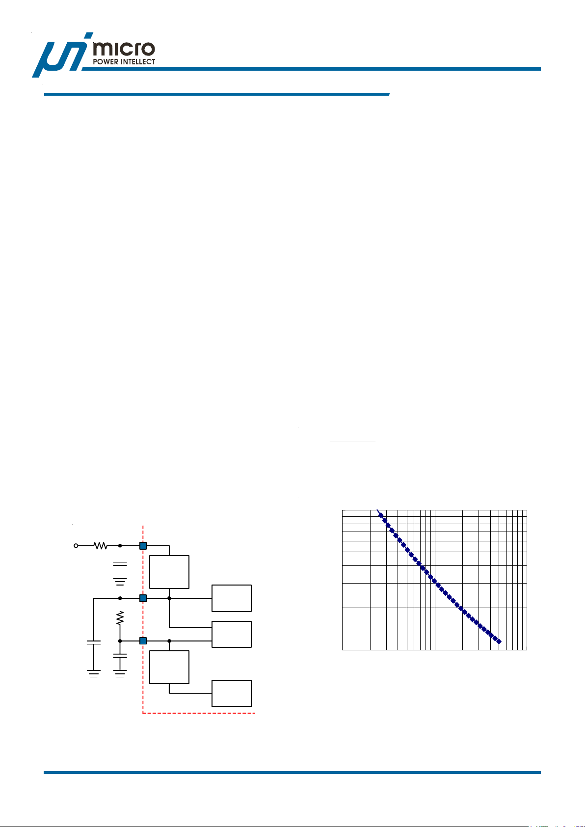
Supply Voltage
The uP6161 is designed to work with a single supply rail.
It integrates two linear regulators providing optimal supply
voltages for gate drivers a nd control circuitry respectively
as shown in Figure 1. The 9V linear regulator generates
9V PVCC9 for gate drives achieving optimum balance
between efficiency a nd thermal management. The 5V linear
regulator works with VCC9 input generates VCC5 for
internal control circuitry . If 12V driving voltage is preferred,
simply connect +12V to the PVCC9 pin and let VCC12
open.
power on reset with typical rising threshold level a s 7.5V.
All the three supply inputs require minimum 1uF ceramic
capa citors f or local bypassing. Pla ce the bypa ss ca pacitors
physically near the IC. No external bypass capacitor is
required for filtering the VCC5 voltage.
Bootstrap Circuitry
The uP6161 integrates MOSFET gate drives that are
powered from the PVCC9 pin and support 12V+12V driving
capa bility . A bootstra p diode is embedded to facilitate s PCB
design and reduce the total BOM cost. Connect a cera mic
bootstrap diode between BOOT and PHASE pins to f orm a
bootstra p circuit for providing charge to turn on/off the upper
MOSFET. No external Schottky diode is required.
Converters that consist of uP6161 feature high efficiency
without special consideration on the selection of
MOSFETs.
Chip Enable and Frequency Setting
The RT/DIS is a multifunctional pin: chip shutdown and
frequency setting. Pulling low this pin to GND by a n open
drain/collector transistor shuts down the uP6161 and
disables both buck and line ar controllers.
The switching frequency is set by a resistor connecting to
the RT/DIS pin a s:
f
OSC
23500000
R
RT
74000
+=
(Hz)
Figure 2 shows the dependence between the resistor
chosen and the resulting switching frequency .
1000
+12V
VCC12
PVCC9
VCC9
9V
Linear
Regulator
uP6161
Gate
Drivers
POR
Monitoring
Switching Frequency (kHz
100
5V
Linear
Regulator
Control
Circuitry
10 100 1000
(kohm)
R
RT
Figure 2. Switching Frequency vs. R
RT
Soft Start
Figure 1. Supply V oltage Configuration
Once POR is acknowledged and RT/DIS pin is released,
Both PVCC9 and VCC9 are continuously monitored for
uPI Semiconductor Corp., http://www.upi-semi.com
Rev. P00, File Name: uP6161-DS-P0001
5
Page 6
Preliminary
uP6161
Functional Description
the uP6161 initiates its digital soft start cycle to prevent
surge current from power supply input during turn on
(referring to the Functional Block Diagram). The error
amplif iers are three-input devices. Reference voltage V
REF
or the internal soft start voltage SS2/SS3 whichever is
smaller dominates the behavior of the non-inverting inputs
of the error amplifiers. SS2/SS3 intern ally ramps up to 0.8V
in 4096 cycles of the internal oscillator frequency after the
after the softstart cycle is initiated. Take 600kHz switching
frequency for exa mple (1.67us per cycle), the ramp-up ti me
is about 6.8ms. Accordingly , the output voltages follow the
soft start signals SS2/SS3 and linearly ramp up to their
final level, resulting minimum inrush current from input
voltage.
The SS2/SS3 signals keep ramping up after it exceeds
the internal 0.8V reference voltages. However , the internal
0.8V reference voltages takes over the behavior of error
amplif ier after SS > V
. When the SS2/SS3 signal climb
REF
to its ceiling voltage (5V), the uP6161 claims the end of
softstart cycle and ena ble the under voltage protection of
the output voltages.
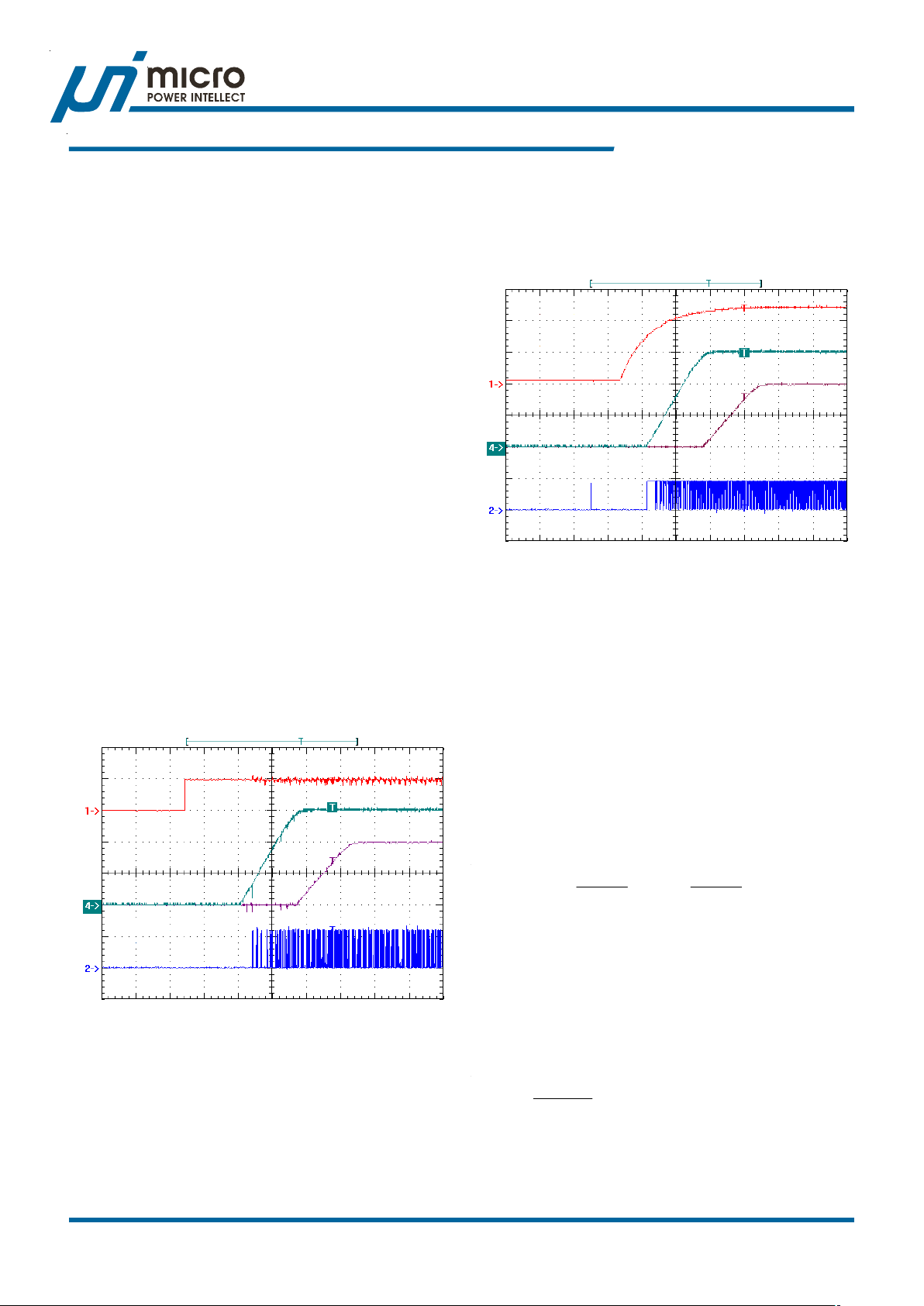
Figure 3 shows a typical start up interval for uP6161 where
the RT/DIS pin ha s been relea sed from a grounded (system
shutdown) state. Note the LDO output voltage (LVO)
starts ramping up only after the PWM output voltage
(SVO) is within regulation.
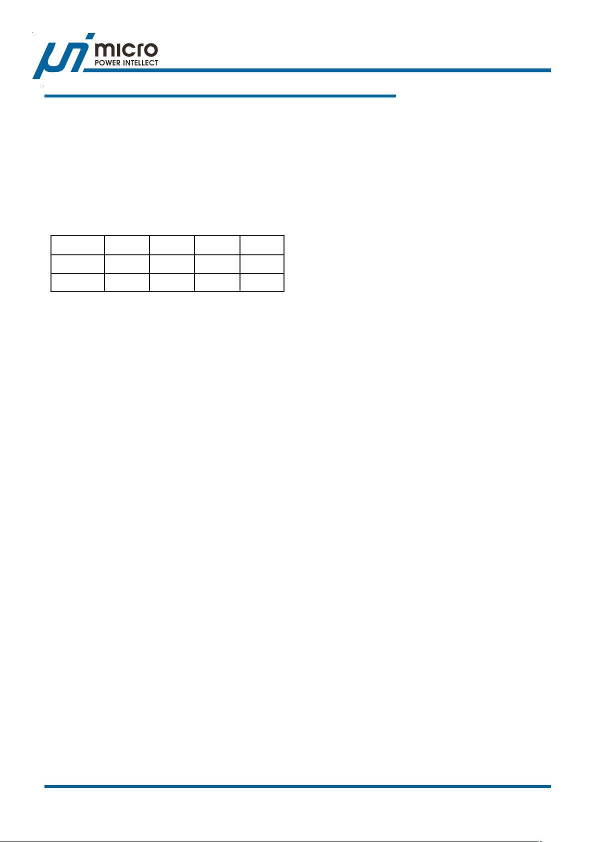
ramping up to 5VDD. Another softstart is initiated after SS
ramps up to 5V DD. The hiccup period is about 8ms. Figure
4 shows the start up interval where VIN does not present
initially.
SVO
(0.5V /Div)
LVO
(0.5V/ D iv)
(5V/D iv )
LGATE
(10V/Div)
V
IN
Time (5ms/Div)
Figure 4. Softstart where VIN does not Present Initially.
Output Voltage Selection
The output voltage can be progra mmed to any level between
the 0.8V internal reference, up to the 80% of VIN supply.
The lower limitation of output voltage is caused by the
internal reference. The upper limitation of the output voltage
is caused by the maximum available duty cycle (80%
typical). This is to leave enough time for overcurrent
detection. Output voltage out of this range is not allowed.
RT/DIS
(1V/Div)
SVO
(0.5V /D iv )
LVO
(0.5V /Div)
PHASE
(10V/Div)
Time (5ms/Div)
Figure 3. Softstart Behavior.
Power Input Detection
The uP6161 detects PHASE voltage for the present of power
input when the UGA TE turns on the first ti me. If the PHASE
voltage does not exceed 2.0V when the UGA TE turns on,
the uP6161 asserts that power in put in not ready and stops
the softstart cycle. However, the internal SS continues
uPI Semiconductor Corp., http://www.upi-semi.com
Rev. P00, File Name: uP6161-DS-P0001
A voltage divider sets the output voltage (refer to the Typical
Application Circuit on page 1 for detail). In real a pplications,
choose R2 in 100Ω ~ 10kΩ range a nd choose appropri ate
R1 according to the desired output voltage.
+
×=
VV
REFOUT
2R1R
2R
+
×=
V8.0
2R1R
2R
Overcurrent Protection (OCP)
The uP6161 detects voltage drop across the lower MOSFET
(V
) for overcurrent protection when it is turned on. If
PHASE
V
is lower than the user-progra mmable voltage V
PHASE
OCP
the uP6161 asserts OCP and shuts down the converter.
The OCP level can be calculated according the onresistance of the lower MOSFET used.
V
I −=
OCP
OCP
R
)ON(DS
(A)
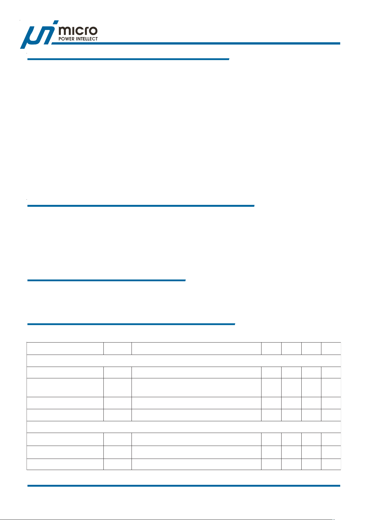
Connecting a resistance from LGATE to GND selects the
,
6
Page 7
Preliminary
uP6161
Functional Description
appropri ate V
1 is OCP level if a lower MOSFET with 10mΩ R
as shown in T a ble 1. Also shown in T a ble
OCP
DS(ON)
is
used.
When programming the OCP level, take into con sideration
the conditions that affect R
of the lower MOSFET,
DS(ON)
including operation junction temperature, gate driving voltage
and distribution. Consider the R
at maximum operation
DS(ON)
temperature and lowest gate driving voltage.
T able 1. OCP Level Selection
R
(Ω)nepok24k42k01
PCO
V
I
)Vm(573-003-522-051-
PCO
)A(5.73525.2251
PCO
Another factor should ta ken into consideration is the ripple
of the inductor current. The current near the valley of the
ripple current is used for OCP, resulting the averaged OCP
level a little higher than the calculated value.
Output Under V oltage Protection of Line ar Regulator
The LDRV and LFB voltages are monitored during both
softstart and normal operation for output under voltage
protection. The uP6161 a sserts UVP if the error a mplifier
saturates, LDRV goes to ceiling high and LFB voltage is
lower than 0.6V for 10us. This demands V
CC12
> (V
OUT
+
VTH + 1V) where VTH is the threshold voltage of the external
N-Channel MOSFET. This is to ensure that the output
voltage can follow the softstart sign al and will not saturate
the error amplifier. That means a low threshold voltage
MOSFET is required for low V
demands that V
should be ready before the soft start
IN2
applications. This also
CC12
cycle is initiated.
The uP6161 disables the output voltages upon the triggering
of UVP . The uP6161 re peats the softstart cycle if the output
under voltage is not removed.
uPI Semiconductor Corp., http://www.upi-semi.com
Rev. P00, File Name: uP6161-DS-P0001
7
Page 8
Preliminary
A
g
n
uP6161
bsolute Ma x imum Ratin
Supply Input Voltage, VCC12 (Note 1) -------------------------------------------------------------------------------------------- -0.3V to +15V
PHASE to GND
DC ------------------------------------------------------------------------------------------------------------------------------------- -1V to 15V
< 200ns ---------------------------------------------------------------------------------------------------------------------------- -3V to 30V
BOOT to PHASE ---------------------------------------------------------------------------------------------------------------------------- -0.3V to +15V
UGA TE to PHASE ------------------------------------------------------------------------------------------------ -0.3V to (BOOT - PHASE +0.3V)
PVCC9, VCC9, LDRV ----------------------------------------------------------------------------------------------------- -0.3V to VCC12 + 0.3V
LGA TE ------------------------------------------------------------------------------------------------------------------------ -0.3V to + (PVCC9 + 0.3V)
Other Pins -------------------------------------------------------------------------------------------------------------------------------------- -0.3V to +6V
Storage T emperature Range ------------------------------------------------------------------------------------------------------------- -65OC to +150OC
Junction T emperature ------------------------------------------------------------------------------------------------------------------------------------ 150OC
Lead T emperature (Soldering, 10 se c) ------------------------------------------------------------------------------------------------------------ 260OC
ESD Rating (Note 2)
HBM (Human Body Mode) --------------------------------------------------------------------------------------------------------------------- 2kV
MM (Machine Mode) ----------------------------------------------------------------------------------------------------------------------------- 200V
Thermal Informatio
Pack age Thermal Resistance (Note 3)
θ
SOP-14 ------------------------------------------------------------------------------------------------------------------------------ 120°C/W
JA
θ
QF N3x3-16 ----------------------------------------------------------------------------------------------------------------------------- 5OC/W
JC
θ
QF N3x3-16 ---------------------------------------------------------------------------------------------------------------------------- 68OC/W
JA
Power Dissipation, PD @ TA = 25°C
SOP-14 ----------------------------------------------------------------------------------------------------------------------------------------------- 0.83W
QF N3x3-16 ------------------------------------------------------------------------------------------------------------------------------------------ 1.47W
Recommen de d Op er at i o n Condition s
Operating Junction T emperature Ra nge (Note 4) ------------------------------------------------------------------------ -40°C to +125°C
Operating Ambient T emperature Range -------------------------------------------------------------------------------------- -40°C to +85°C
Supply Input V oltage, V
----------------------------------------------------------------------------------------------------------- +10.8V to 13.2V
CC12
Electrical Characteristics
(V
= 12V, TA = 25OC, unless otherwise specified)
CC12
retemaraPlobmySsnoitidnoCtseTniMpyTxaMstinU
tupnIylppuS
egatloVylppuSV
tnerruCylppuSI
21CC
21CC
gnihctiwS
V;nepOETAGLdnaETAGU
21CC
,V21=
8.01--2.31V
--4--Am
tnerruCylppuStnecseiuQI
egatloVtupnIrewoPV
VBFV=
Q_21CC
1NI
teseRnOrewoP
dlohserhTROP21CCVV
dlohserhTROP9CCVPV
siseretsyHROPV
uPI Semiconductor Corp., http://www.upi-semi.com
Rev. P00, File Name: uP6161-DS-P0001
HTR21CC
HTR9CCV
SYH9CC
FER
gnihctiwSoN,V1.0+--3--Am
0.32.31V
--7.8--V
gnisir9CCV=9CCVP--5.78V
gnillaf9CCV=9CCVP--8.0--V
8
Page 9
Preliminary
uP6161
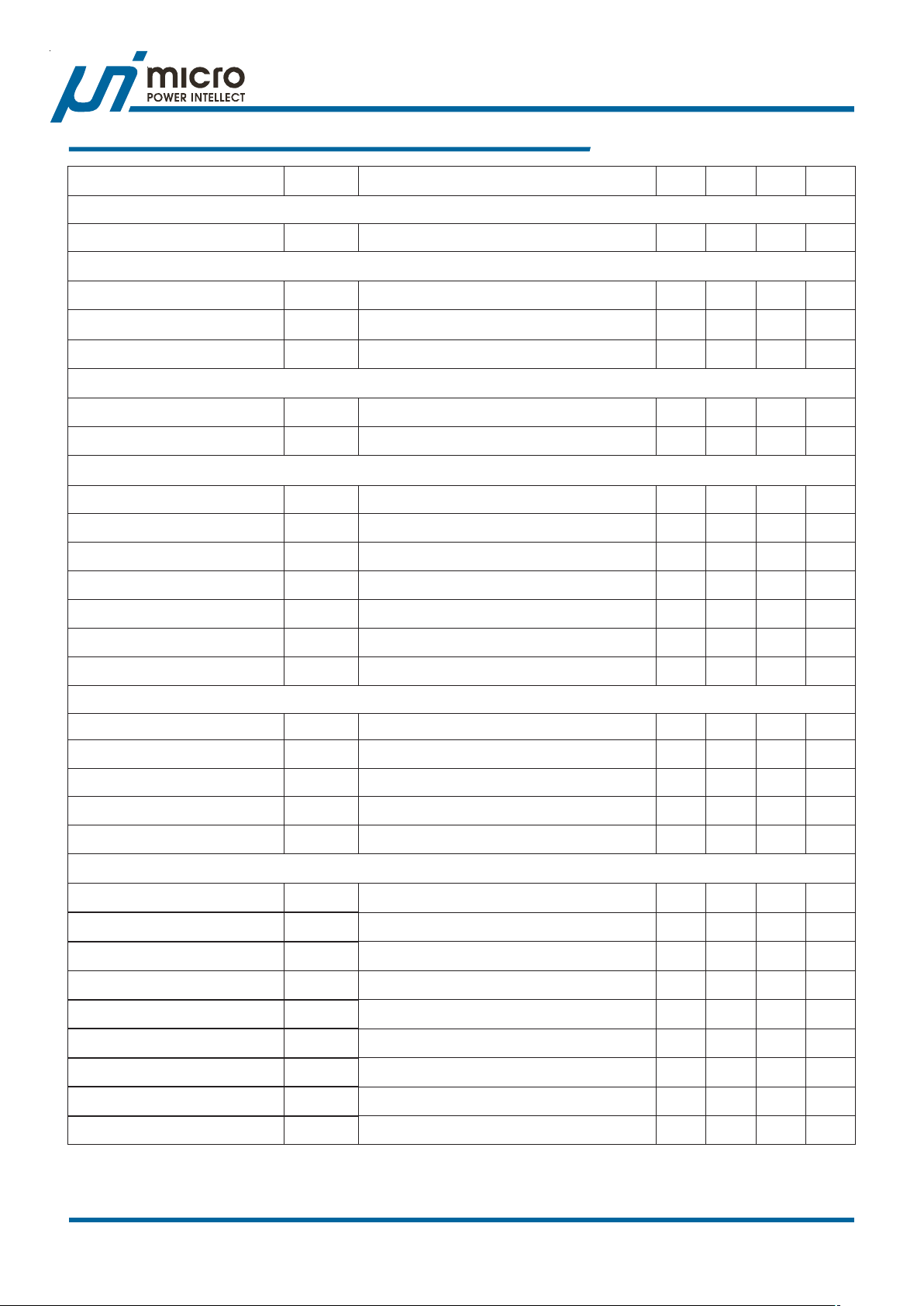
Electrical Characteristics
retemaraPlobmySsnoitidnoCtseTniMpyTxaMstinU
ODL9CCVP
egatloVtuptuO9CCVP9CCVPV
V21=--0.9--V
21CC
tratStfoSdnarotallicsO
ycneuqerFgnihctiwSf
edutilpmAhtootwaS ΔV
lavretnItratStfoST
R
CSO
SS
TR
CSO
f
CSO
k3.54= Ω 045026007zHk
--4--V
zHk026=--8.6--sm
egatloVecnerefeR
MWProfegatloVecnerefeRV
ODLrofegatloVecnerefeRV
FER
FER
887.08.0218.0V
487.08.0618.0V
rellortnoCkcuBrofreifilpmArorrE
niaGCDpooLnepOA
O
ngiseDybdeetnarauG5507--Bd
tcudorPhtdiwdnaB-niaGPWBGngiseDybdeetnarauG--01--zHM
etaRwelSRSngiseDybdeetnarauG46--su/V
tloVtuptuOhgiHPMOCV
ega
egatloVtuptuOwoLPMOCV
tnerruCecruoShgiHPMOCI
V/
BF
FER
)V
V(leveLegatlovrednU
H_PMOC
L_PMOC
H_PMOC
PVU
srevirDetaGrellortnoCkcuB
--7.4--V
--6.0--V
--8.2---Am
075708%
tnerruCecruoSETAGUI
ecnadepmItuptuOkniSETAGUR
tnerruCecruoSETAGLI
ecnadepmItuptuOkniSETAGLR
VP
CRS_GU
VP
KNS_GU
VP
CRS_GL
VP
KNS_GL
V,V9=
V-
CC
CC
CC
CC
TOOB
I,V9=
GU
V,V9=
GL
I,V9=
GL
V8=--5.1---A
GU
Am001=--24Ω
V1=--5.1---A
Am001=--24Ω
elcyCytuDmumixaM 075708%
rellortnoCrotalugeR-raeniL
niaGCDpooLnepOA
O
ngiseDybdeetnarauG5507--Bd
tcudorPhtdiwdnaB-niaGPWBGngiseDybdeetnarauG--2--zHM
etaRwelSRSngiseDybdeetnarauG24--su/V
ruCsaiBBFI
tner
egatloVtuptuOhgiHVRDLV
egatloVtuptuOwoLVRDLV
tnerruCecruoShgiHVRDLI
tnerruCkniSwoLVRDLI
V/
BFL
)V
FER
V(leveLegatlovrednU
V
BF
PVU
BF
H_VRDL
L_VRDL
H_VRDL
L_VRDL
V8.0=--10.01Au
V9=CCVP--5.80.9V
V9=CCVP--0.05.0V
5----Am
5----Am
lanimoNfotnecreP075708%
uPI Semiconductor Corp., http://www.upi-semi.com
Rev. P00, File Name: uP6161-DS-P0001
9
Page 10

Preliminary
uP6161
Electrical Characteristics
retemaraPlobmySsnoitidnoCtseTniMpyTxaMstinU
noitcetorP
dlohserhTtnerruCrevOV
dlohserhTelbanEV
Note 1. Stresses listed a s the above “Absolute Maximum Ratings” may cause permanent damage to the device.
These are for stress ratings. Functional operation of the device at the se or any other conditions beyond those
indicated in the operational sections of the specifications is not implied. Exposure to absolute maximum
rating conditions for extended periods may remain possibility to af fect device relia bility .
Note 2. Devices are ESD sensitive. Handling pre caution recommended.
Note 3. θJA is mea sured in the natural convection at TA = 25°C on a low effective thermal conductivity test board of
JEDEC 51-3 thermal mea surement standard.
Note 4. The device is not guaranteed to function outside its operating conditions.
R
ESAHP
SID/TR
ETAGL
nepo=--573---Vm
3.04.05.0V
uPI Semiconductor Corp., http://www.upi-semi.com
Rev. P00, File Name: uP6161-DS-P0001
10
Page 11
Preliminary
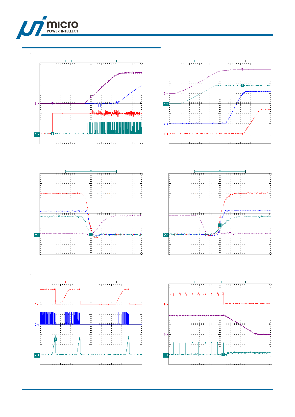
Typical Operation Characteris tics
uP6161
RT/DIS
(0.5V/Div)
UGATE
(5V/Div)
T urn On Waveforms
SV
OUT
(0.5V/Div)
(0.5V/Div)
(10V/Div)
2.5ms/Div
Gate Waveforms
LV
OUT
PHASE
Power On Waveforms
PVCC9
(5V/Div)
5ms/Div
Gate Waveforms
(5V/Div)
VCC12
(5V/Div)
SV
(0.5V/Div)
LV
(0.5V/Div)
UGATE
OUT
OUT
PHASE
(5V/Div)
UGATE-PHASE
(5V/Div)
Over Current Protection
25ns/Div
(0.5V/Div)
PHASE
(10V/Div)
SV
OUT
I
OUT
(10A/Div)
LGATE
(5V/Div)
LGATE
(5V/Div)
PHASE
(5V/Div)
UGATE-PHASE
(5V/Div)
25ns/Div
Trun Off Wavef orms
RT/DIS
(1V/Div)
LDRV
(2V/Div)
PHASE
(10V/Div)
10ms/Div
uPI Semiconductor Corp., http://www.upi-semi.com
Rev. P00, File Name: uP6161-DS-P0001
5us/Div
11
Page 12
Preliminary
Typical Operation Characteris tics
uP6161
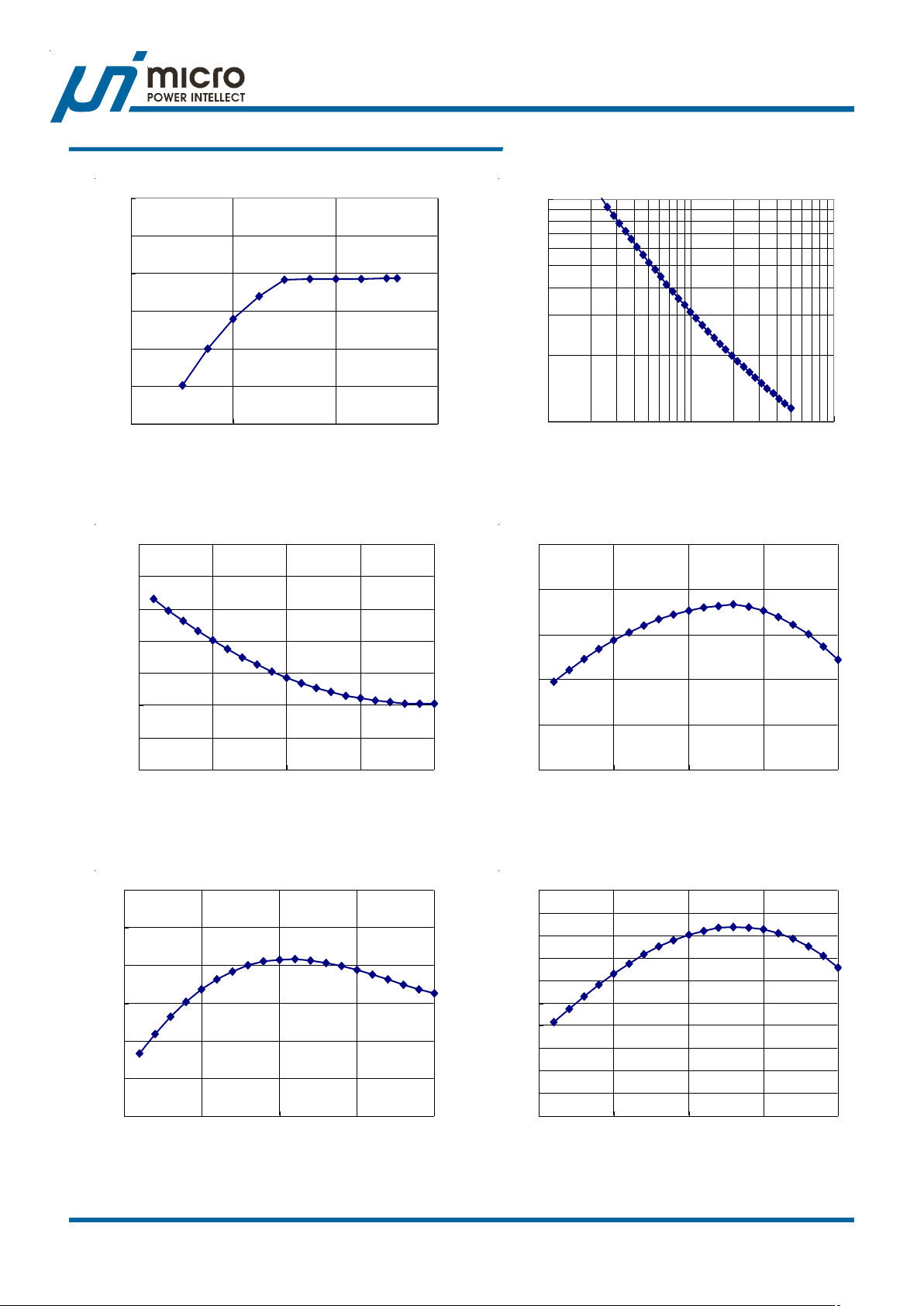
PVCC9 V oltage vs. VCC12 Voltage
10
9.5
9
8.5
8
PVCC9 V oltage (V)
7.5
7
8101214
VCC12 V oltage (V)
PVCC9 Voltage vs. Temperature
9.07
9.06
9.05
9.04
Switching Frequency vs. R
1000
Switching Frequency (kHz)
100
10 100 1000
RRT (kΩ)
DC/DC Output V oltage vs. Temperature
0.5
0.2
-0.1
RT
9.03
9.02
PVCC9 Output V oltage (V)
9.01
9
-50 0 50 100 150
Junction Temperature (OC)
VCC12 = 12V
Switching Frequency vs. Temperature
2
1
0
-1
-2
-3
Switching Frequency Variation (%)
-4
-50 0 50 100 150
Junction Temperature (OC)
-0.4
-0.7
DC/DC Output Voltage Variation (%)
-1
-50 0 50 100 150
Junction Temperature (OC)
LDO Output V oltage vs. Temperature
0.5
0.3
0.1
-0.1
-0.3
-0.5
-0.7
-0.9
-1.1
-1.3
LDO Output Voltage Variation (%)
-1.5
-50 0 50 100 150
Junction Temperature (OC)
uPI Semiconductor Corp., http://www.upi-semi.com
Rev. P00, File Name: uP6161-DS-P0001
12
Page 13

Preliminary
A
pplication I nformation
This page is intentionally left blank a nd will be updated when the silicon data is available.
uP6161
uPI Semiconductor Corp., http://www.upi-semi.com
Rev. P00, File Name: uP6161-DS-P0001
13
Page 14
n
0.76 REF 1.27 REF
6.15 REF
8.00 MIN
Preliminary
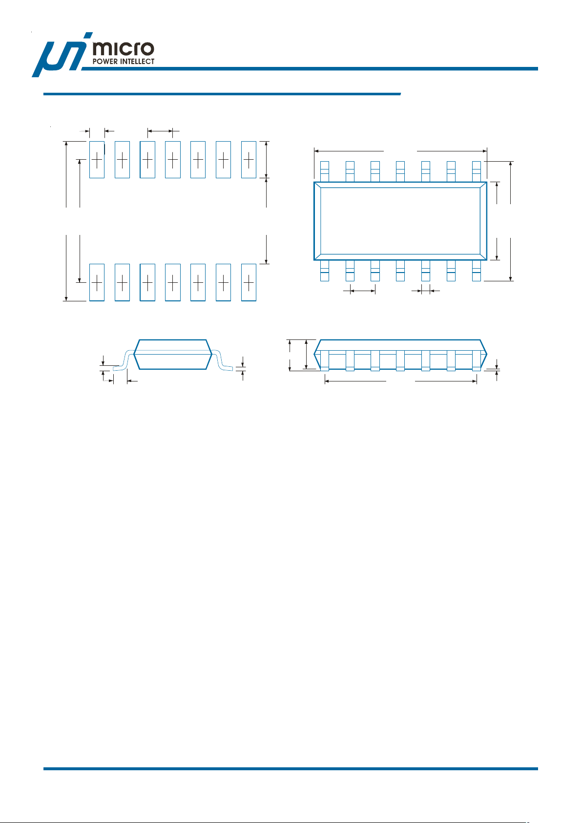
SOP-14 Package
1.85 REF
4.00 MIN
uP6161
Package Informatio
8.50 - 8.75
5.80 - 6.20
3.80 - 4.00
1.27 BSC
0.32 - 0.52
Recommended Solder Pad Layout
1.45 - 1.60
0.20 BSC
0.41 - 0.89
0.18 - 0.25
1.75 MAX
0.10 - 0.25
7.62 BSC
Note
1.Pa ckage Outline Unit Description:
BSC: Basic. Re presents theoretical exa ct dimen sion or dimen sion target
MIN: Minimum dimension specified.
MAX: Maximum dimension specified.
REF: Reference. Represents dimension f or reference use only . This value is not a device specification.
TYP . Typical. Provided a s a general value. This value is not a device spe cification.
2.Dimensions in Millimeters.
3.Drawing not to scale.
4.These dimensions no not include mold flash or protrusions. Mold flash or protrusion s shell not exceed 0.15mm.
uPI Semiconductor Corp., http://www.upi-semi.com
Rev. P00, File Name: uP6161-DS-P0001
14
Page 15
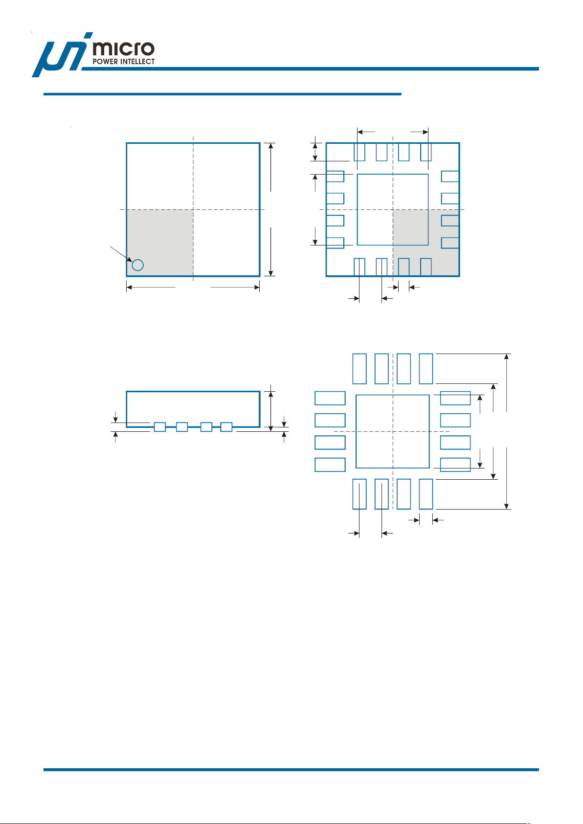
Preliminary
n
QFN3x3 - 16L Package
uP6161
Package Informatio
Pin 1 mark
(Note 6)
2.90 - 3.10
2.90 - 3.10
0.80 - 1.00
0.35 - 0.45
1.50 - 1.75
1.50 - 1.75
9
13
5
1
0.18 - 0.30
0.50 BSC
Bottom View - Exposed Pad
3.45 - 3.55
2.10 - 2.20
1.60 - 1.70
0.20 - REF
0.00 - 0.05
0.20 - 0.30
0.50 BSC
Recommended Solder Pitch and Dimensions
Note
1.Pa ckage Outline Unit Descri ption:
BSC: Basic. Re presents theoretical exa ct di mension or dimen sion target
MIN: Minimum dimension specified.
MAX: Maximum dimension specified.
REF: Reference. Represents dimension f or reference use only . This value is not a device specification.
TYP . Typical. Provided a s a general value. This value is not a device spe cification.
2.Dimensions in Millimeters.
3.Drawing not to scale.
4.These dimension s no not include mold fla sh or protrusions. Mold fla sh or protrusions shell not exceed 0.15mm.
uPI Semiconductor Corp., http://www.upi-semi.com
Rev. P00, File Name: uP6161-DS-P0001
15
 Loading...