

Page 1
uP6109
A
5V/12V Synchronous-Rectif ied
Buck Controller with Ena ble Input
General Description
The uP6109 is a compact synchronous-rectified buck
controller specifically designed to operate from 5V or 12
supply voltage and to deliver high quality output volt age a s
low as 0.8V. This (P)SOP-8 device operates at fixed 300
kHz frequency and provides a n optimal level of integration
to reduce size and cost of the power s upply.
This controller integrates internal MOSFET drivers that
support 12V+12V bootstra pped voltage f or high efficiency
power conversion. The bootstra p diode is built-in to simpli fy
the circuit design a nd minimize external part count.
Other features include internal softstart, undervoltage
protection, overcurrent protection and s hutdown function.
With aforementioned functions, this part provides
customers a compact, high ef ficiency, well-protected and
cost-effective solutions. This part is available in (P)SOP-8
packages.
Ordering Information
rebmuNredrOepyTegakcaPkrameR
8ASA9016Pu8-POS
8USA9016Pu8-POSP
Note: uPI products are compatible with the current IPC/
JEDEC J-ST D-020 and RoHS requirements. They are 100%
matte tin (Sn) plating and suit a ble f or use in SnPb or Pbfree soldering processes.
Features
Operate from 5V or 12V Supply Voltage
3.3V to 12V VIN Input Range
0.8 V
Output Range from V
Simple Single-Loop Control Design
Voltage-Mode PWM Control
Fast T ran sient Respon se
High-Bandwidth Error Amplifier
0% to 80% Duty Cycle
Lossless, Programma ble Overcurrent Protection
Uses Lower MOSFET R
300 kHz Fixed Frequency Oscillator
Internal Soft Start
Integrated Bootstra p Diode
with 1.5% Accuracy
REF
to 80% of V
REF
DS(ON)
IN
pplications
Power Supplies for Microprocessors or
Subsystem Power Supplies
Cable Modems, Set Top Boxes, and xDSL
Modems
Industrial Power Supplies; General Purpose
Supplies
5V or 12V Input DC-DC Regulators
Low Voltage Distributed Power Supplies
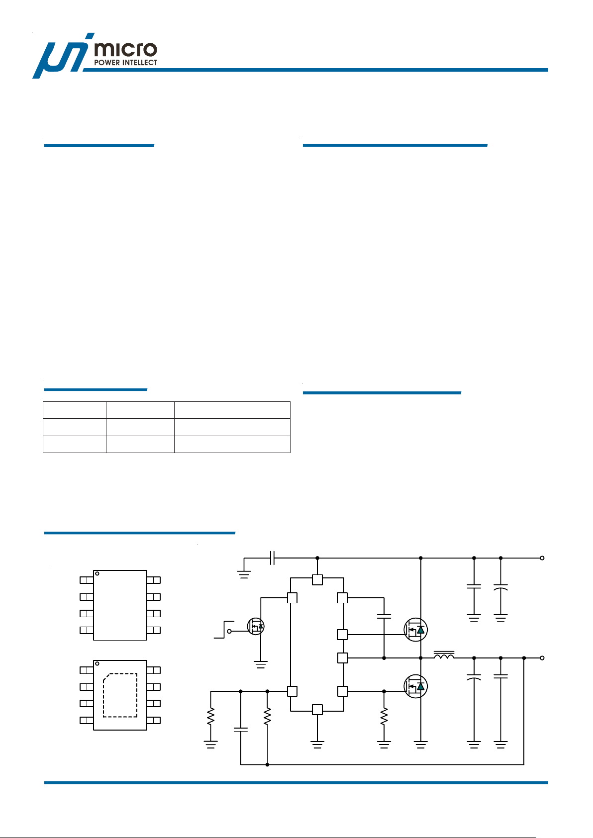
Pin Configuration & Typical Application Circuit
1
UGATE
GND
LGATE
UGATE
GND
LGATE
uPI Semiconductor Corp., http://www.upi-semi.com
Rev. F00, File Name: uP6109-DS-F0000
2
3
45
SOP-8
1
2
GND
3
45
PSOP-8
PHASEBOOT
8
EN
7
FB
6
VCC
PHASEBOOT
8
EN
7
FB
6
VCC
Disable
Enable
Option
EN
FB
V
IN
VCC
5
BOOT
uP6109
3
GND
1
2
8
4
UGATE
PHASE
LGATE
V
OUT
1
7
6
Page 2

.oNemaNniPnoitcnuFniP
n
uP6109
Function al Pin Descriptio
1TOOB
2ETAGU
3DNG
4ETAGL
5CCV
6BF
7NE
ylppuSpartstooB CroticapacpartstoobehttcennoC.revirdetagreppugnitaolfehtrof
ehtnonrutotegrahcehtsedivorpC
CtahterusnE.Fu74.0
TOOB
.tuptuOrevirDetaGreppU derotinomsinipsihT.TEFSOMreppufoetagehtotnipsihttcennoC
.ffodenrut
orGrewoPdnalangiS .nipsihtottcepserhtiwderusaemeraslevelsegatlovllA
.tuptuOrevirDetaGrewoL derotinomsinipsihT.TEFSOMrewolf
htyb
.ffo
.egatloVylppuS ehT.revirdetagrewolehtdna9016PuehtrofylppussaibehtsedivorpnipsihT
.CI
.egatloVkcabdeeF morfredividrotsiserA.reif
siDNGottuptuoeht
.elbanEpihC otrota
,pots
.CIehtrofdnu
.CIehtraendecalpsi
ehthguorhtenalp/dnalsidnuorgehtotnipsihteiT
oetagehtotnipsihttcennoC
.woldlehebotstuptuoETAGLdnaETAGUeht
rofseulavlacipyT.TEFSOMreppu
TOOB
gnilpuocedatahterusnE.nipsihtotegatlovylppusV2.31otV5.4
ilpmarorreehtottupnignitrevniehtsinipsihT
.retrevnocehtfopoolkcabdeeflortnocegatlovehtetasnepmocotnipNE/PMOC
TOOB
roticapacpartstoobehT.tiucricpartstoobamrofotnipESAHPehtdnanipTOOBneewteb
otFu1.0morfegnar
ahTEFSOMreppuehtnehwenimretedotyrtiucricnoitcetorphguorht-toohsevitpadaehtyb
s
.elbaliavanoitcennocecnadepmitsewol
nrutsahTEFSOMrewolehtnehwenimretedotyrtiucricnoitcetorphguorht-toohsevitpadae
lewatcennoC.tiucriclortnoclanretnirofDDV4otdetalugeryllanretnisiegatlovylppus
delpuoced-l
ehtraendecalpsiroticapac
ehthtiwnoitanibmocninipsihtesU.egatlovnoitalugerehttesotdesu
llicsoehtsesuacdnarellortnocehtselbasidV3.0nahtrewolnipsihtgnilluP
8ESAHP
.edoNhctiwSESAHP ehtfoniardehtdnaTEFSOMreppuehtfoecruosehtotnipsihttcennoC
tdna,revirdETAGUehtrofknisehtsadesusinipsihT.TEFSOMrewol
revorofTEFSOMrewolehtssorcapord
oohsevitpada
ewopaninommocsihcihwegatlov
.metsysylppusr
egatlovehtrotinomo
ehtybderotinomoslasinipsihT.noitcetorptnerruc
.ffodenrutsahTEFSOMreppuehtnehwenimretedotyrtiucricnoitcetorphguorht-t
tneisnartevitagenecuderotdednemmocersidnuorgdnanipsihtneewtebedoidykttohcSA
uPI Semiconductor Corp., http://www.upi-semi.com
Rev. F00, File Name: uP6109-DS-F0000
2
Page 3

VCC
5
uP6109
Functional Block Diagram
FB
EN
Internal
Regulator
4VDD
V
PWM
OCP
Gate
Control
Logic
VCC
Soft
Start
SS
6
Error
0.8V
Amplifier
VCC
30K
7
0.3V
Enable
POR
Oscillator
OCP
Comparator
3
GND
1
2
8
4
BOOT
UGATE
PHASE
LGATE
uPI Semiconductor Corp., http://www.upi-semi.com
Rev. F00, File Name: uP6109-DS-F0000
3
Page 4

uP6109
Functional Description
The uP6109 is a compact synchronous-rectified buck
controller specifically designed to operate from 5V or 12
supply voltage and to deliver high quality output volt age a s
low as 0.8V. This (P)SOP-8 device operates at fixed 300
kHz frequency and provides a n optimal level of integration
to reduce size and cost of the power supply.
Supply Voltage
The VCC pin receives a well-decoupled 4.5V to 13.2V
supply voltage to power the uP6109 control circuit, the
lower gate driver and the bootstrap circuit for the higher
gate driver. A minimum 0.1uF ceramic capacitor is
recommended to bypass the supply voltage. Place the
bypassing capacitor physically near the IC.
An internal linear regulator regulates supply voltage into a
4.0V voltage 4VDD for internal control logic circuit. No
external bypa ss capa citor is required for f iltering the 4.0V DD
voltage.
The uP6109 integrates MOSFET gate drives that are
powered from the VCC pin a nd support 12V+12V driving
capa bility. A bootstra p diode is embedded to f acilit ates PCB
design and reduce the total BOM cost. No external
Schottky diode is required. Converters that consist of
uP6109 feature high efficiency without special consideration
on the selection of MOSFETs.
Note: The embedded bootstra p diode is not a Schott ky
diode having a 0.7V forward voltage. External
Schottky diode is highly recommended if the VCC
voltage is expected to be lower than 5.0V. Otherwise
the bootstrap diode may be too low for the device to
work normally.
Power On Reset and Chip Enable
A power on reset (POR) circuitry continuously monitors
the supply voltage at VCC pin. Once the rising POR
threshold is exceeded, the uP6109 sets itself to active
state and is ready to accept chip enable command. The
rising POR threshold is typically 4.2V at VCC rising.
VCC
uP6109
30kohm
EN
0.3V
Disable
Enable
Enable
Figure 1. Enable Implementation of uP6109.
SoftStart
A built-in Soft Start is used to prevent surge current from
power supply input during turn on (referring to the Functional
Block Di agra m). The error a mplifier is a three-input device.
Reference voltage V
or the internal soft start voltage SS
REF
whichever is smaller dominates the behavior of the noninverting input of the error a mplifier . SS internally ra mps up
to 4VDD in 50ms after the softstart cycle is initiated. The
ramp i s created digitally , so there will be 100 small di screte
steps. Accordingly, the output voltage will follow the SS
signal a nd ramp up smoothly to its target level.
The SS signal keeps ra mping up after it exceeds the internal
reference V
over the behavior of error a mpli fier after SS > V
. However , the reference volt age V
REF
REF
REF
takes
. When
the SS signal climb to its ceiling voltage (5V), the uP6109
claims the end of softstart cycle and enable the under
voltage protection of the output voltage.
For internal reference voltage, the ef fective ra mp-up time of
the output voltage is about 3.6ms.
For the uP6109 (300kHz operation frequency), the soft start
is about 2.4ms.
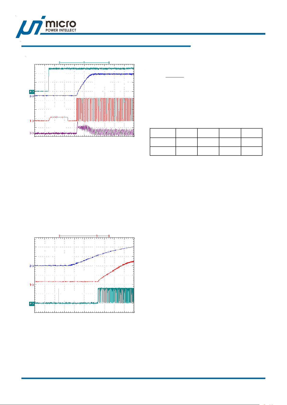
Figure 2 shows a typical start up interval where the EN pin
has been released from a grounded (system shutdown)
state.
The EN pin is internally pulled high to VCC by a 30kΩ
resistor as shown in Figure 1. A signal level NPN or
NMOSFET transistor is adequate to pull this lower than
0.3V to shut down the device. When EN pin is relea sed, it
is pulled high and cla mped to about 1.0V by internal zener
diode.
uPI Semiconductor Corp., http://www.upi-semi.com
Rev. F00, File Name: uP6109-DS-F0000
4
Page 5
V
IN
5V/Div
LGATE
5V/Div
V
OUT
0.5V/Div
uP6109
Functional Description
OCP level can be calculated a ccording t he on-resist a nce
of the lower MOSFET used.
V
I −=
OCP
Connecting a resista nce from LGATE to GND selects t he
appropri ate V
1 is OCP level if a lower MOSFET with 10mΩ R
used.
OCP
R
)ON(DS
a s shown in Table 1. Also s hown in Table
OCP
(A)
DS(ON)
is
I
X
2.5/Div
2ms/Div
Figure 2. Softstart Behavior .
Power Input Detection
The uP6109 detects PHASE voltage for the present of power
input when the UGA TE turns on the f irst time. If the PHASE
voltage does not exceed 3.0V when the UGA TE turn s on,
the uP6109 a sserts that power input in not ready a nd stops
the softstart cycle. However, the internal SS continues
ra mping up to 4V DD. Anot her softstart is initi ated after SS
ra mps up to 4VDD. The hiccup period is about 12ms. Figure
3 shows the start up interval where VIN does not present
initially.
V
IN
5V/Div
T a ble 1. OCP Level Selection
R
(Ω)nepok24k62k01
PCO
V
I
)Vm(573-003-522-051-
PCO
)A(5.73035.2251
PCO
When progra mming the OCP level, t ake into consi deration
the conditions that affect R
of the lower MOSFET,
DS(ON)
including operation junction temperature, gate driving voltage
and distri bution. Consider the R
at maximum operation
DS(ON)
temperature and lowe st gate driving voltage.
Another fa ctor should t aken into con sideration is the ripple
of the inductor current. The current near the valley of the
ripple current is used for OCP, res ulting the averaged OCP
level a little higher tha n the calculated value.
Undervoltage Protection (UVP)
The FB voltage is monitored for undervoltage protection.
The UVP threshold level is typical 0.6V for both standalone and tracking mode. The uP6109 shuts down upon
the detection of UVP and can be reset only by POR or
toggling EN pin.
V
OUT
5V/Div
LGATE
5V/Div
1ms/Div
Figure 3. Softstart where VIN doe s not Present Initially.
Overcurrent Protection (OCP)
The uP6109 detects voltage drop a cross the lower MOSFET
(V
) for overcurrent protection when it is turn on. If V
PHASE
is lower than the user-programmable voltage V
OCP
PHASE
, the
uP6109 asserts OCP and shuts down the converter. The
uPI Semiconductor Corp., http://www.upi-semi.com
Rev. F00, File Name: uP6109-DS-F0000
5
Page 6
uP6109
A
g
n
bsolute Ma x imum Ratin
Supply Input Voltage, VCC (Note 1) ------------------------------------------------------------------------------------------------ -0.3V to +15V
PHASE to GND
DC ------------------------------------------------------------------------------------------------------------------------------------- -5V to 15V
< 200ns ---------------------------------------------------------------------------------------------------------------------------- -5V to 30V
BOOT to PHASE -------------------------------------------------------------------------------------------------------------------------------------- 15V
BOOT to GND
DC ------------------------------------------------------------------------------------------------------------------------- -0.3V to PHASE +15V
< 200ns -------------------------------------------------------------------------------------------------------------------------- -0.3V to 42V
Input, Output or I/O Voltage ---------------------------------------------------------------------------------------------------------- -0.3V to +6V
Storage T emperature Ra nge ------------------------------------------------------------------------------------------------------------- -65OC to +150OC
Junction T emperature ------------------------------------------------------------------------------------------------------------------------------------ 150OC
Lead T emperature (Soldering, 10 sec) ------------------------------------------------------------------------------------------------------------ 260OC
ESD Rating (Note 2)
HBM (Huma n Body Mode) --------------------------------------------------------------------------------------------------------------------- 2kV
MM (Machine Mode) ----------------------------------------------------------------------------------------------------------------------------- 200V
Thermal Informatio
Package Thermal Resistance (Note 3)
SOP-8 θJA----------------------------------------------------------------------------------------------------------------------------------- 160°C/W
PSOP-8 θJA---------------------------------------------------------------------------------------------------------------------------------- 50°C/W
PSOP-8 θJC---------------------------------------------------------------------------------------------------------------------------------- 15°C/W
Power Dissipation, PD @ TA = 25°C
SOP-8 ------------------------------------------------------------------------------------------------------------------------------------------- 0.625W
PSOP-8 ------------------------------------------------------------------------------------------------------------------------------------------------- 2.0W
Recommen de d Op er at i o n Conditi on s
Operating Junction T emperature R ange (Note 4) ------------------------------------------------------------------------ -40°C to +125°C
Operating Ambient Temperature Range -------------------------------------------------------------------------------------- -40°C to +85°C
Supply Input Volt age, V
---------------------------------------------------------------------------------------------------------------- +4.5V to 13.2V
CC
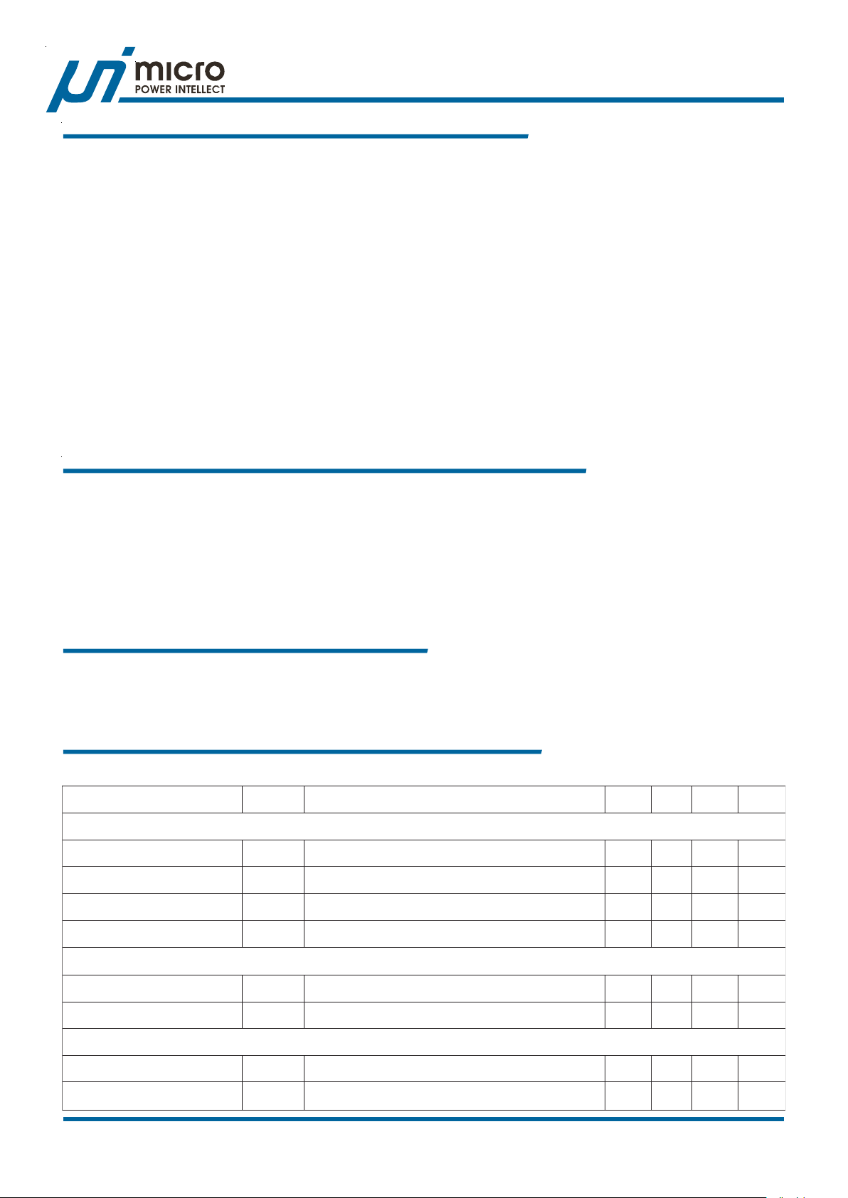
Electrical Characteristics
(VCC = 12V, TA = 25OC, unless otherwise specified)
retemaraPlobmySsnoitidnoCtseTniMpyTxaMstinU
tupnIylppuS
egatloVylppuSV
tnerruCylppuSI
egatloVtupnIrewoPV
CC
CC
tnerruCylppuStnecseiuQI
NI
V
Q_CC
BF
teseRnOrewoP
dlohserhTROPV
siseretsyHROPV
V
HTRCC
SYHCC
gnisir0.42.44.4V
CC
rotallicsO
V;nepOETAGL,ETAGU
CC
gnihctiwS,V21=--4--Am
gnihctiwSoN,V9.0=--3--Am
5.4--2.31V
0.3--2.31V
--2.0--V
ycneuqerFgninnuReerFf
CSO
edutilpmApmaR ΔV
uPI Semiconductor Corp., http://www.upi-semi.com
Rev. F00, File Name: uP6109-DS-F0000
V
CC
V
CSO
CC
V21=552003543zHk
V21=--5.1--V
P-P
6
Page 7
uP6109
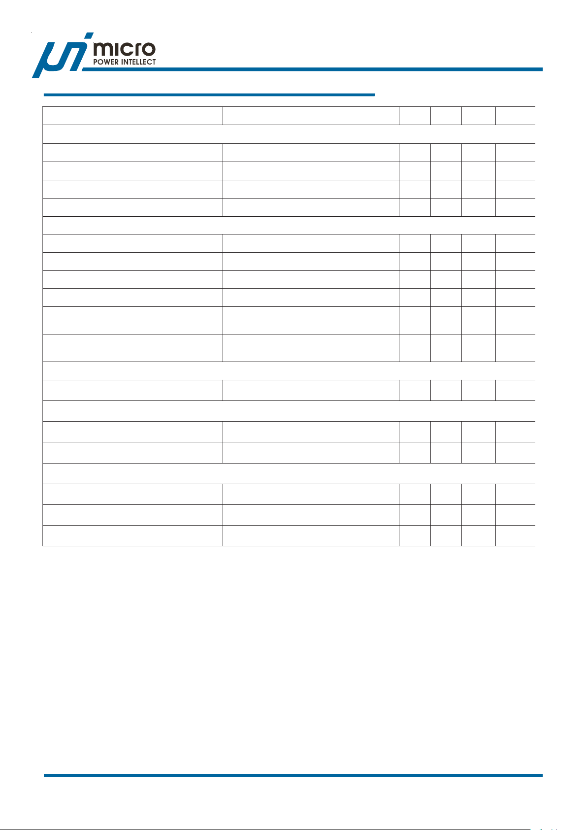
Electrical Characteristics
retemaraPlobmySsnoitidnoCtseTniMpyTxaMstinU
reifilpmArorrE
niaGCDpooLnepOOAngiseDybdeetnarauG5507--Bd
aB-niaGWBGngiseDybdeetnarauG--01--zHM
tcudorPhtdiwdn
etaRwelSRSngiseDybdeetnarauG36--su/V
ecnatcudnocsnarTngiseDybdeetnarauG----7.0Sm
srevirDetaGrellortnoCMWP
V
V
VCCVV
V
CC
V
CC
V-
TOOB
ESAHP
V-
ETAGU
ETAGL
ESAHP
ETAGL
V1.0=--24 Ω
V;V21=
V;V21=
V2.1>)
tnerruCgnicruoSetaGreppUI
RetaGreppU
gnikniSR
)NO(SD
tnerruCgnicruoSetaGrewoLI
RetaGrewoL
gnikniSR
)NO(SD
CRS_GU
KNS_GU
CRS_GL
KNS_GL
gnisiRETAGLotgnillaFESAHP
yaleD
gnisiRETAGUotgnillaFETAGL
yaleD
egatloVecnerefeR
egatloVkcabdeeFlanimoNV
BF
dlohserhTelbanE
dlohserhTelbanEV
dlohserhTelbasiDV
V
HTRNE
HTFNE
NE
V
NE
.gnisir6.0----V
.gnillaf----3.0V
V,V21=
V-
TOOB
V6=--1---A
ETAGU
V1.0=--24Ω
V6=--1---A
ESAHP
ETAGL
VotV2.1<
V(otV2.1<
V2.1>--03--sn
ETAGL
V-
ETAGU
ESAHP
--03--sn
edoMenolAdnatS887.08.0218.0V
noitcetorP
noitcetorPegatloVrednUV
dlohserhTtnerruCrevOV
lavretnItratS-tfoST
PVU_BF
R
ESAHP
SS
nepO--573---Vm
ETAGL
55.06.056.0V
4.26.38.4sm
Note 1. Stresses listed a s the a bove “Absolute Maximum R atings” may cause permanent d amage to the device.
These are for stress ratings. Functional operation of the device at t hese or a ny other conditions beyond those
indicated in the operational sections of the specifications is not implied. Exposure to absolute maximum
rating conditions for extended periods may remain possibility to af fect device relia bility .
Note 2. Devices are ESD sensitive. H andling precaution re commended.
Note 3. θJA is mea sured in the n atural convection at TA = 25°C on a low effective ther mal conductivity test board of
JEDEC 51-3 ther mal mea surement st and ard.
Note 4. The device is not guaranteed to f unction outside its operating conditions.
uPI Semiconductor Corp., http://www.upi-semi.com
Rev. F00, File Name: uP6109-DS-F0000
7
Page 8
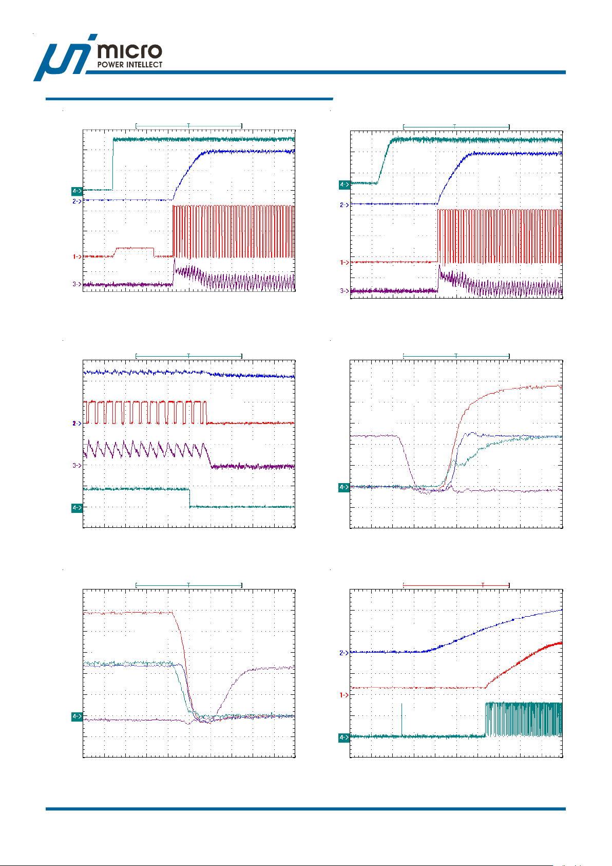
uP6109
Typical Operation Characteristics
V
IN
Power On Waveforms
V
IN
5V/Div
LGATE
5V/Div
I
X
2.5/Div
2ms/Div
=12V, V
= 1.2V, C
OUT
Turn Off Waveforms
V
OUT
0.5V/Div
= 1500uF, No Load
OUT
V
0.5V/Div
LGATE
10V/Div
OUT
Turn On Waveforms
EN
0.5V/Div
LGATE
5V/Div
I
X
2.5A/Div
V
OUT
0.5V/Div
2ms/Div
V
=12V, V
IN
= 1.2V, C
OUT
= 1500uF, No Load
OUT
Switching Wavefor ms: UGA TE Turn On
UGATE
5V/Div
LGATE
5V/Div
PHASE
5V/Div
I
X
10A/Div
EN
1V/Div
10us/Div
V
= 12V , V
IN
= 1.2V , C
OUT
= 1500uF, I
OUT
OUT
= 6A
Switching Wavefor ms: UGA TE Trun Off
UGATE
5V/Div
UGATE - PHASE
5V/Div
PHASE
5V/Div
LGATE
5V/Div
UGATE - PHASE
5V/Div
25ns/Div
VIN = 12V , I
OUT
= 10A
Power Sequencing Operation
V
IN
5V/Div
V
OUT
5V/Div
LGATE
5V/Div
25ns/Div
VIN = 12V , I
OUT
= 10A
uPI Semiconductor Corp., http://www.upi-semi.com
Rev. F00, File Name: uP6109-DS-F0000
V
=12V Ready , V
CC
1ms/Div
= 1.2V, C
OUT
= 1500uF, No Load
OUT
8
Page 9

uP6109
Typical Operation Characteristics
Load T ra n sient Re spon se
I
OUT
10A/Div
V
OUT
5V/Div
10us/Div
V
=12V , V
IN
= 1.2V, C
OUT
OUT
Over Current Protection
V
OUT
0.5V/Div
PHASE
5V/Div
I
X
20A/Div
PHASE
10V/Div
= 1500uF
Over Current Protection
V
OUT
0.5V/Div
PHASE
5V/Div
I
X
20A/Div
5ms/Div, V
= 12V, V
IN
Turn On to Short Circuit
= 1.2V, C
OUT
= 1500uF,
OUT
Line Regulation
0.5
0.4
0.3
0.2
0.1
0
-0.1
-0.2
-0.3
-0.4
Output Voltage Deviation (%)
-0.5
4 6 8 101214
5ms/Div, V
= 12V, V
IN
Output Short to Ground
= 1.2V, C
OUT
= 1500uF,
OUT
Load Regulation
0.3
0.2
0.1
0
-0.1
-0.2
-0.3
-0.4
-0.5
Output Voltage Deviation (%)
-0.6
-0.7
0 5 10 15 20 25 30
Output Current (A)
uPI Semiconductor Corp., http://www.upi-semi.com
Rev. F00, File Name: uP6109-DS-F0000
Input V oltage (V)
Output V oltage vs. Junction Temperature
3
2.5
2
1.5
1
0.5
0
-0.5
-1
-1.5
-2
Output V oltage Varition (%)
-2.5
-3
-50 -25 0 25 50 75 100 125
Junction Temperature (OC)
9
Page 10
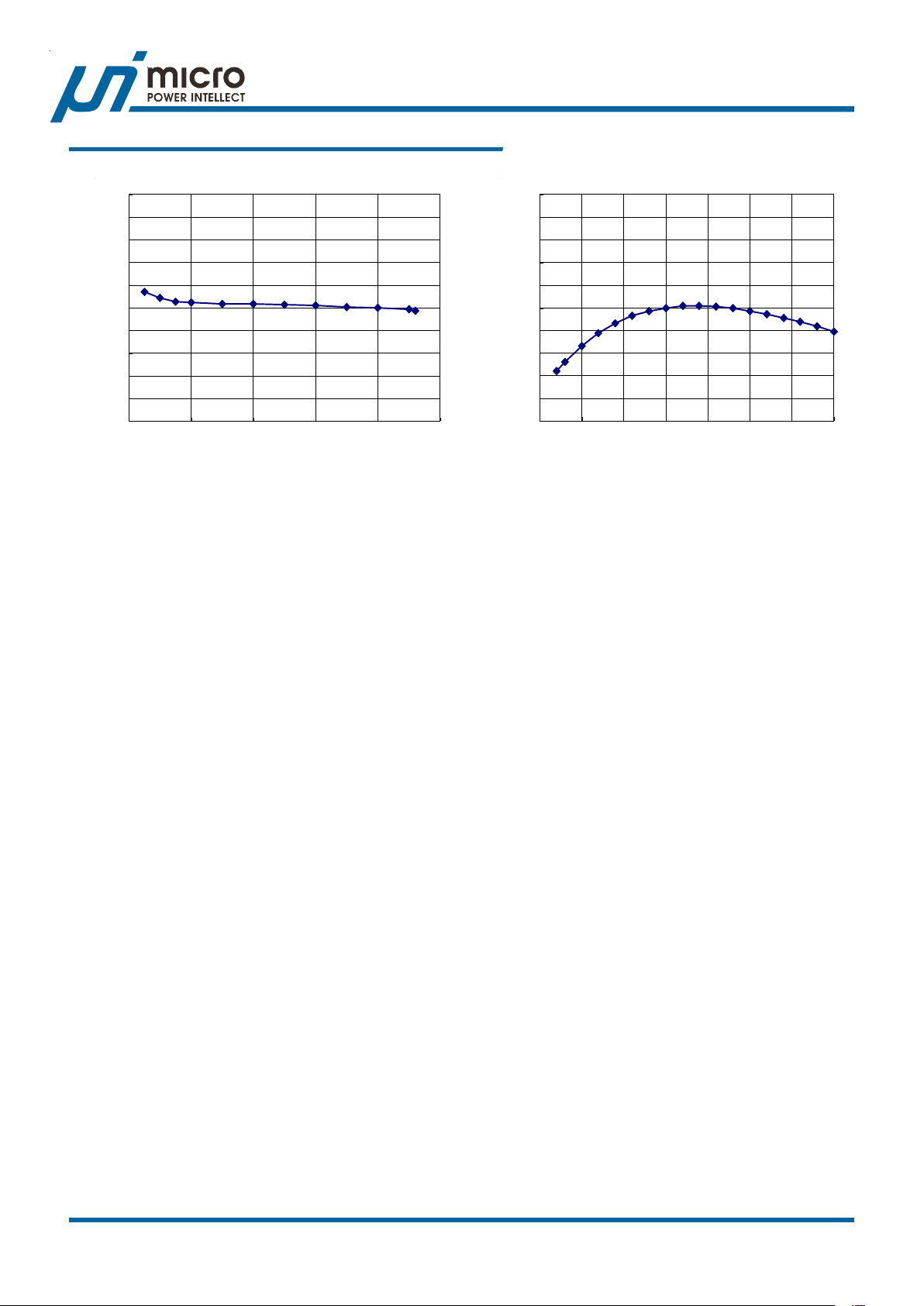
uP6109
Typical Operation Characteristics
Switching Frequency vs. Input Voltage
225
220
215
210
205
200
195
190
185
Switching Frequency (kHz)
180
175
468101214
Input V oltage (V)
Switching Frequency vs. Junction Temperature
225
220
215
210
205
200
195
190
185
Switching Frequency (kHz)
180
175
-50 -25 0 25 50 75 100 125
Junction Temperature (OC)
uPI Semiconductor Corp., http://www.upi-semi.com
Rev. F00, File Name: uP6109-DS-F0000
10
Page 11

uP6109
A
pplication I nformation
Power MOSFET Selection
External component selection is primarily determined by
the maximum load current a nd begins with t he selection of
power MOSFET switches. The uP6109 requires two
external N-channel power MOSFE T s for upper (controlled)
and lower (synchronous) switches. Importa nt para meters
for the power MOSFE T s are the brea kdown voltage V
on-resistance R
maximum current I
, reverse transfer capacitance C
DS(ON)
, gate supply requirements, and
DS(MAX)
(BR)DSS
RSS
ther mal manage ment requirements.
The gate drive voltage is powered by VCC pin that receives
4.5V~13.2V supply voltage. When operating with a 12V
power supply for VCC (or down to a minimum supply
voltage of 8V), a wide variety of NMOSFETs can be used.
Logic-level threshold MOSFET should be used if the input
voltage is expected to drop below 8V. Since the lower
MOSFET i s used as t he current sensing element, particular
attention must be paid to its on-resista nce. Look for R
DS(ON)
ratings at lowest gate driving voltage.
Special cautions should be exercised on the lower switch
exhibiting very low threshold voltage V
. The shoot-
GS(TH)
through protection present aboard the uP6109 may be
circumvented by these MOSFETs if they have large
para sitic impeda nces and/or ca pa cita nces that would inhibit
the gate of the MOSFET from being discharged below its
threshold level before the complementary MOSFET is
turned on. Also avoid MOSFE T s wit h excessive switching
times; the circuitry is expecting tra nsitions to occur in under
50 nsec or so.
In high-current applications, the MOSFET power
dissipation, package selection and heatsink are the
dominant design factors. The power dissipation includes
two loss components; conduction loss and switching loss.
The conduction losses are the largest component of power
dissipation for both the upper and the lower MOSFETs.
These losses are distributed between the two MOSFETs
according to duty cycle. Since t he uP6109 is operating in
continuous conduction mode, the duty cycles for the
MOSFETs is:
D =
UP
V
OUT
V
IN
D
=
LO
;
VV
−
OUTIN
V
IN
The resulting power dissipation in the MOSFETs at
maximum output current are:
2
OUTUP
2
OUTLO
DRIP ××=
LO)ON(DS
fTVI5.0DRIP ××××+××=
OSCSWINOUTUP)ON(DS
where TSW is the combined switch ON a nd OFF time.
Both MOSFETs have I2R losses and the top MOSFET
includes an addition al term f or switching losses, which are
largest at high input voltages. The bottom MOSFET losses
are greatest when the bottom duty cycle is near 100%,
during a short-circuit or at high input voltage. These
equations a ssume linear voltage current tran sitions a nd do
not adequately model power loss due the reverse-recovery
,
of the lower MOSFET’s body diode. Ensure that both
,
MOSFETs are within their maxi mum junction temperature
at high ambient te mperature by calculating the temperature
rise according to package thermal-resistance
specifications. A separate heatsink may be necessary
depending upon MOSFET power, package type, a mbient
temperature and air flow .
The gate-charge losses are dissipated by t he uP6109 and
don’t heat the MOSFETs. However, large gate charge
increases the switching interval, TSW that increases the
MOSFET switching losses. The gate-charge losses are
calculated as :
G
CC
where C
ISS_UP
MOSFET, C
MOSFET, and C
is the input capacitance of the upper
is the input capacitance of the lower
ISS_LO
RSS_UP
is the reverse tran sfer ca pa citance
of the upper MOSFET. Ma ke sure that t he gate-charge loss
will not cause over temperature at uP6109, especially with
large gate cap acita nce a nd high supply voltage.
Output Inductor Selection
Output inductor selection usually is based the
considerations of inductance, rated current, size
requirement, and DC resist ance (DC)
Given t he desired in put a nd output volt ages, t he inductor
value and operating frequency deter mine the ri pple current:
=Δ
I
L
1
×
Lf
OUTOSC
OUT
V
OUT
−××
1(V
)
V
IN
Lower ripple current reduces core losses in the inductor,
ESR losses in the output capacitors and output voltage
ripple. Highest efficiency operation is obtained at low
frequency with small ripple current. H owever, a chieving this
requires a large inductor. There is a tradeoff between
component size, efficiency and operating frequency. A
rea sonable st arting point is to choose a ripple current th at
is about 40% of I
OUT(MAX)
.
There is another tradeoff between output ripple current/
voltage and re sponse ti me to a tra nsient load. Increasing
the value of inducta nce reduces t he output ripple current
and voltage. H owever, t he large inducta nce values reduce
the converter’s respon se time to a load tra nsient.
f)CV)CC(V(VP ××++××=
OSCRSSINLO_ISSUP_ISSCC
uPI Semiconductor Corp., http://www.upi-semi.com
Rev. F00, File Name: uP6109-DS-F0000
11
Page 12

uP6109
A
pplication I nformation
Maximum current ratings of the inductor are generally
specified in two methods: permissible DC current and
saturation current. Per missible DC current is the allowable
DC current that causes 40OC temperature raise. The
saturation current is the allowable current that causes 10%
inductance loss. Make sure that the inductor will not
saturate over the operation conditions including temperature
range, input voltage ra nge, a nd maximum output current.
The size requirements refer to the area and height
requirement for a particular design. For better eff iciency,
choose a low DC resistance inductor. DCR is usually
inversely proportional to size.
Different core materials a nd shapes will change the size/
current and price/current relations hip of an inductor . Toroid
or shielded pot cores in ferrite or permalloy materials are
small and don’t radiate much energy, but generally cost
more tha n powdered iron core inductors with similar electrical
characteristics. The choice of which style inductor to use
often depends more on the price vs. size requirements
and a ny radiated field/EMI requirements.
Input Capacitor Selection
The synchronous-rectified buck converter draws pulsed
current with sharp edge s from the input ca pa citor resulting
in ripples and spikes at the input supply voltage. Use a
mix of input bypass capacitors to control the voltage
overshoot across the MOSFETs. Use small ceramic
capa citors for high frequency decoupling a nd bulk capa citors
to supply the current needed each time upper MOSFET
turns on. Place the small ceramic capacitors physically
close to the MOSFETs and between the drain of upper
MOSET and the source of lower MOSFET to avoid the
stray inductance along t he connection tra ce.
The importa nt parameters for the bulk input ca pacitor are
the voltage rating a nd the RMS current rating. For relia ble
operation, select the bulk ca pa citor with voltage and current
ratings above the maximum input volt age and largest RMS
current required by the circuit. The ca pa citor voltage rating
should be at least 1.25 times greater than the maximum
input voltage and a voltage rating of 1.5 times is a
conservative guideline. The RMS current rating requirement
for the input ca pa citor of a buck converter is calculated a s:
manufacturer’s ripple current ratings are often based on
2000 hours of life. This ma kes it advisable to f urther derate
the capacitor, or choose a capacitor rated at a higher
temperature tha n required. Always con sult the manuf acturer
if there is a ny que stion.
For a through-hole design, several electrolytic ca pacitors
may be needed. For surfa ce mount designs, solid ta ntalum
ca pacitors ca n also be used, but caution must be exercised
with regard to the capacitor surge current rating. These
ca pa citors must be ca pable of h a ndling the surge-current
at power-up. Some ca pacitor series availa ble from reputable
manuf a cturers are surge current tested.
Output Capacitor Selection
An output ca pacitor is required to filter t he output and supply
the load tran sient current. The selection of C
is primarily
OUT
determined by the ESR required to minimize voltage ripple
and load step transients. The output ripple ΔV
OUT
is
a pproximately bounded by:
ESR(IV
+Δ≤Δ
LOUT
1
××
)
Cf8
OUTOSC
Since ΔIL increa ses wit h input voltage, t he output ripple is
highest at maximum input volt age. T ypically, once t he ESR
requirement is satisfied, the capacitance is adequate for
filtering and h as t he necessary RMS current rating. Multi ple
capacitors placed in parallel may be needed to meet the
ESR and RMS current ha ndling requirements. Dry ta ntalum,
special polymer, aluminum electrolytic and ceramic
capacitors are all available in surface mount packages.
Special polymer capacitors offer very low ESR but have
lower ca pa cita nce density t ha n ot her types.
The load transient require ments are a function of the slew
rate (di/dt) and t he magnitude of the tran sient load current.
These requirements are generally met with a mix of
capacitors and careful layout. Modern components and
loads are cap able of producing tra nsient load rates above
1A/ns. High frequency capacitors initially supply the
transient and slow the current load rate seen by the bulk
capacitors. The bulk filter capacitor values are generally
deter mined by the ESR (Effective Serie s Resista nce) and
voltage rating requirements rather t han a ctual ca pa citance
requirements.
OUTINOUT
OUT
)VV(V
, where I
IN(RMS)
II
=
)MAX(OUT)RMS(IN
−
V
IN
This for mula ha s a maximum at VIN = 2V
= I
OUT(RMS)
/2. This simple worst-case condition is
commonly used for design because even significant
deviations do not offer much relief. Note th at the ca pa citor
uPI Semiconductor Corp., http://www.upi-semi.com
Rev. F00, File Name: uP6109-DS-F0000
High frequency decoupling ca pa citors should be placed as
close to the power pins of the load a s physically possible.
Be careful not to add inductance in t he circuit board wiring
that could ca ncel the usefulness of these low inductance
components. Consult with t he manuf acturer of t he load on
12
Page 13

uP6109
A
pplication I nformation
specific decoupling requirements.
Use only specialized low-ESR capacitors intended for
switching-regulator application s for the bulk ca pa citors. The
bulk capacitor’s ESR will determine the output ripple
voltage and t he initial voltage drop after a high slew-rate
transient. An aluminum electrolytic ca pa citor’s ESR value
is related to the case size with lower ESR available in
larger case size s.
However , the Equivalent Series Induct ance (ES L) of these
capacitors increases with case size and can reduce the
usefulness of the capacitor to high slew-rate transient
loading.
Unf ortunately , ESL is not a speci fied para meter . Work with
your capacitor supplier and measure the capacitor’s
impeda nce with frequency to select a suita ble component.
In most cas es, multiple electrolytic ca pa citors of small ca se
size perfor m better th a n a single large ca se capacitor .
Bootstra p Ca pa citor Selection
An external bootstrap capacitor C
BOOT pin supplies the gate drive voltage for the upper
MOSFET. This capacitor is charged through the internal
diode when the PHASE node is low. When the upper
MOSFET turns on, t he PHASE node rises to V
BOOT pin rises to approximately VIN + VCC. The boot
ca pa citor needs to store about 100 times t he gate charge
required by the upper MOSFET. In most a pplications 0.1uF
to 0.47uF , X5R or X7R dielectric ca pa citor is adequate.
PCB Layout Considerations
High speed switching and relatively large pea k currents in
a synchronous-rectified buck converter ma ke the PCB layout
a very importa nt part of design. Fa st current switching from
one device to another in a synchronous-rectified buck
converter causes voltage spikes a cross the interconnecting
impedances and parasitic circuit elements. The voltage
spikes can degrade eff iciency and radiate noise t hat result
in overvoltage stress on devices. Careful component
placement layout a nd printed circuit design mini mizes the
voltage spikes induced in the converter .
Follow the layout guidelines for optimal performance of
uP6109
1 The upper and lower MOSFE T s turn on/off a nd conduct
pulsed current alternatively with high slew rate tra nsition.
Any inductance in t he switched current path generates
a large voltage spike during the switching. The
interconnecting wires indicated by red heavy lines
conduct pulsed current with sharp tra nsient a nd should
be part of a ground or power plane in a printed circuit
board to minimize the voltage spike. Make all the
connection the top layer with wide, copper f illed area s.
connected to the
BOOT
and t h e
IN
2 Place the power components as physically close as
possible.
2.1 Place the input capacitors, especially the highfrequency ceramic de coupling ca pacitors, directly
to the drain of upper MOSFET ad the source of the
lower MOSFET. To reduce the ESR replace the
single input ca pa citor with two parallel units
2.2Place t he output capacitor between the converter
and load.
3 Place t he uP6109 near the upper a nd lower MOSFET s
with pins 1 to 4 facing the power components. Keep
the components connected to pins 4 to 8 close to the
uP6109 and away from the inductor and other noise
sources (noise sensitive components).
4 Use a dedicated grounding plane a nd use via s to ground
all critical components to this layer . The ground pla ne
layer should not have any traces and it should be as
close as possible to the layer with power MOSFETs.
Use an immediate via to connect the components to
ground plane including GND of uP6109 Use several
bigger via s for power components.
5 Apply anot her solid layer a s a power plane a nd cut this
plane into smaller islands of common voltage levels.
The power plane should support the input power and
output power nodes to maintain good voltage filtering
and to keep power losses low . Also, for higher currents,
it is recommended to use a multilayer board to help
with heat sinking power components.
6 The PHASE node is subject to very high dV/dt voltages.
Stray capacitance between this island and the
surrounding circuitry tend to induce current spike a nd
capacitive noise coupling. Keep the sensitive circuit
away from the PHASE node and keep the PCB area
small to limit the ca pa citive coupling. However , the PCB
area should be kept moderate since it also acts as
main heat convection path of the lower MOSFE T.
7 uP6109 sources/sinks impulse current with 2A pea k to
turn on/off the upper and lower MOSFETs. The
connecting trance between the controller and gate/
source of the MOSFET should be wide and short to
minimize the parasitic inductance along the tra ce s.
8 Flood all unused areas on all layers with copper.
Flooding with copper will reduce the temperature rise
of power component.
9 Provide local VCC decoupling between VCC and GND
pins. Locate the ca pa citor, C
to the BOOT and PHASE pins.
a s close as pra ctical
BOOT
uPI Semiconductor Corp., http://www.upi-semi.com
Rev. F00, File Name: uP6109-DS-F0000
13
Page 14
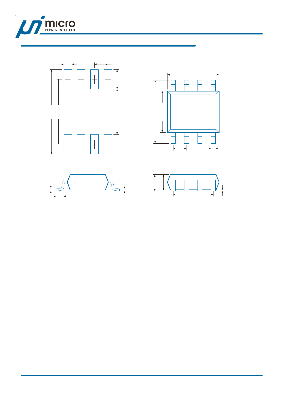
n
SOP - 8 Pack agke
0.76 REF 1.27 REF
1.85 REF
6.15 REF
8.00 MIN
4.00 MIN
5.80 - 6.20
uP6109
Package Informatio
4.80 - 5.00
3.80 - 4.00
1.27 BSC
0.32 - 0.52
Recommended Solder Pad Layout
1.45 - 1.60
0.20 BSC
0.41 - 0.89
0.18 - 0.25
1.75 MAX
0.10 - 0.25
3.81 BSC
Note
1.Package Outline U nit Description:
BSC: Ba sic. Represents t heoretical exa ct di mension or di mension t arget
MIN: Minimum dimension specified.
MAX: Maximum dimension specified.
REF: Reference. Represents di mension for reference use only . This value is not a device speci fication.
TYP . Typical. Provided a s a general value. This value is not a device specification.
2.Dimensions in Millimeters.
3.Drawing not to scale.
4.These dimensions no not include mold flash or protrusions. Mold fla sh or protrusions s hell not exceed 0.15mm.
uPI Semiconductor Corp., http://www.upi-semi.com
Rev. F00, File Name: uP6109-DS-F0000
14
Page 15
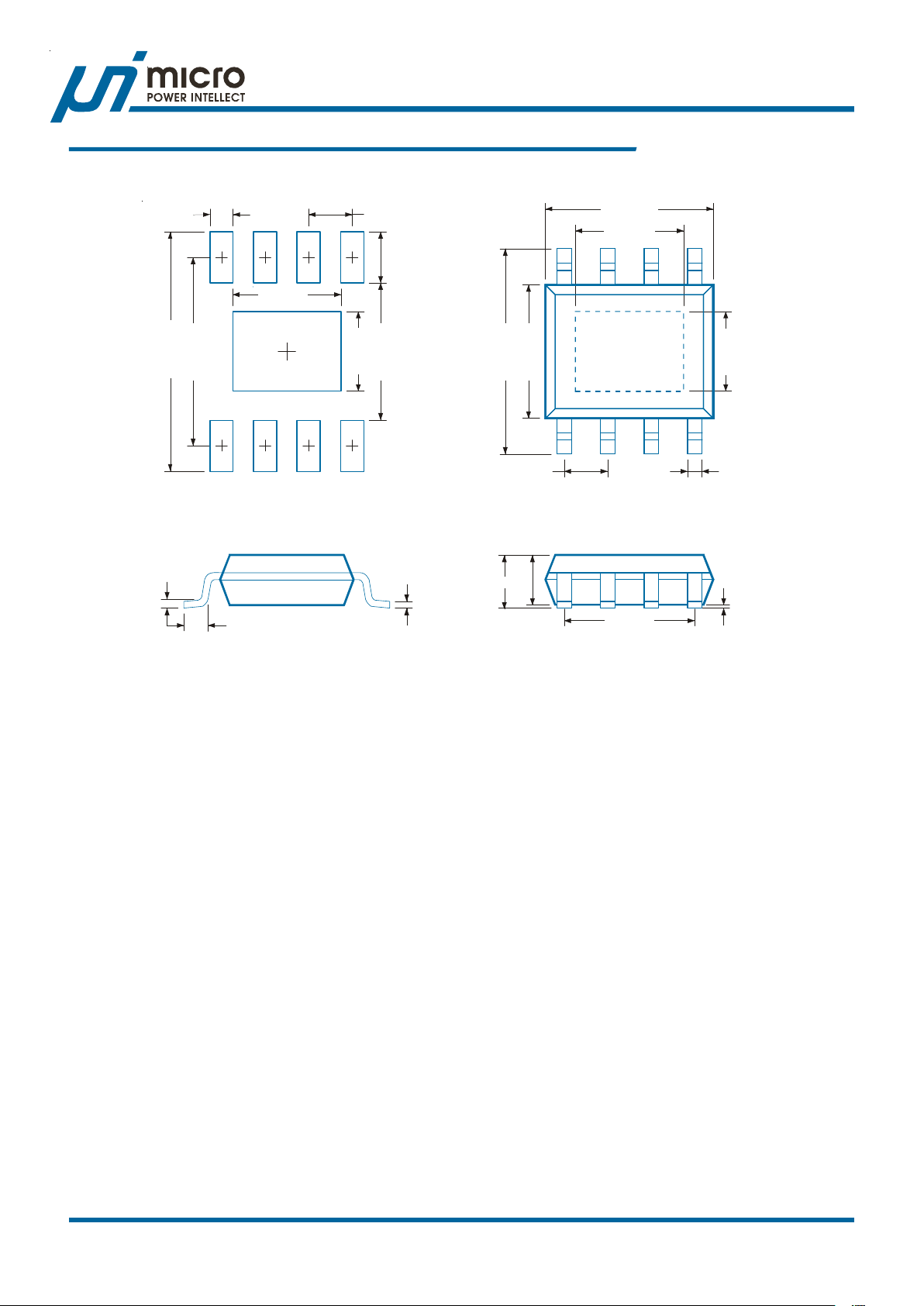
n
PSOP - 8 Packagke
uP6109
Package Informatio
0.70 RE F 1.27 REF
3.00 REF
7.00 REF
5.50 REF
1.50 R EF
2.20 REF
4.00 REF
Recommended Solder Pad Layout
0.20 BSC
0.40 - 0.90
0.18 - 0.25
5.80 - 6.20
1.27 BSC
1.45 - 1.60
1.75 MAX
4.80 - 5.00
3.00 BSC
3.80 - 4.00
3.81 BSC
2.20 BSC
0.32 - 0.52
0.05 - 0.25
Note
1.Package Outline U nit Description:
BSC: Ba sic. Represents t heoretical exa ct di mension or di mension t arget
MIN: Minimum dimension specified.
MAX: Maximum dimension specified.
REF: Reference. Represents dimen sion for reference use only . This value is not a device specif ication.
TYP . Typical. Provided a s a general value. This value is not a device specification.
2.Dimensions in Millimeters.
3.Drawing not to scale.
4.These dimensions no not include mol d fla sh or protrusions. Mol d fla sh or protrusions s hell not exceed 0.15mm.
uPI Semiconductor Corp., http://www.upi-semi.com
Rev. F00, File Name: uP6109-DS-F0000
15
 Loading...