

Page 1
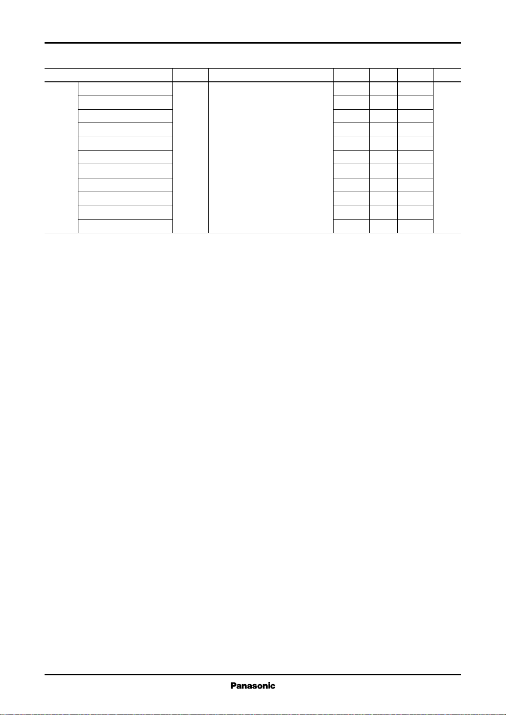
Transistors with built-in Resistor
2.8
+0.2
–0.3
1.5
+0.25
–0.05
0.65±0.15 0.65±0.15
3
1
2
0.950.95
1.9±0.2
0.4
+0.1
–0.05
1.1
+0.2
–0.1
0.8
0.4±0.2
0 to 0.1
0.16
+0.1
–0.06
1.45
0.1 to 0.3
2.9
+0.2
–0.05
B
C
R1
R2
E
UNR2111/2112/2113/2114/2115/2116/2117/2118/2119/2110/
211D/211E/211F/211H/211L/211M/211N/211T/211V/211Z
(UN2111/2112/2113/2114/2115/2116/2117/2118/2119/2110/
211D/211E/211F/211H/211L/211M/211N/211T/211V/211Z)
Silicon PNP epitaxial planer transistor
For digital circuits
Features
■
●
Costs can be reduced through downsizing of the equipment and
reduction of the number of parts.
●
Mini type package, allowing downsizing of the equipment and
automatic insertion through tape packing and magazine packing.
Resistance by Part Number
■
●
UNR211 1 6A 10kΩ 10kΩ
●
UNR2112 6B 22kΩ 22kΩ
●
UNR2113 6C 47kΩ 47kΩ
●
UNR2114 6D 10kΩ 47kΩ
●
UNR2115 6E 10kΩ —
●
UNR2116 6F 4.7kΩ —
●
UNR2117 6H 22kΩ —
●
UNR2118 6I 0.51kΩ 5.1kΩ
●
UNR2119 6K 1kΩ 10kΩ
●
UNR2110 6L 47kΩ —
●
UNR211D 6M 47kΩ 10kΩ
●
UNR211E 6N 47kΩ 22kΩ
●
UNR211F 6O 4.7k Ω 10kΩ
●
UNR211H 6P 2.2kΩ 10kΩ
●
UNR211L 6Q 4.7kΩ 4.7kΩ
●
UNR211M EI 2.2kΩ 47kΩ
●
UNR211N EW 4.7kΩ 47kΩ
●
UNR211T EY 22kΩ 47kΩ
●
UNR211V FC 2.2kΩ 2.2kΩ
●
UNR211Z FE 4.7kΩ 22kΩ
Absolute Maximum Ratings (Ta=25˚C)
■
Parameter Symbol Ratings Unit
Collector to base voltage V
Collector to emitter voltage
Collector current I
Total power dissipation P
Junction temperature T
Storage temperature T
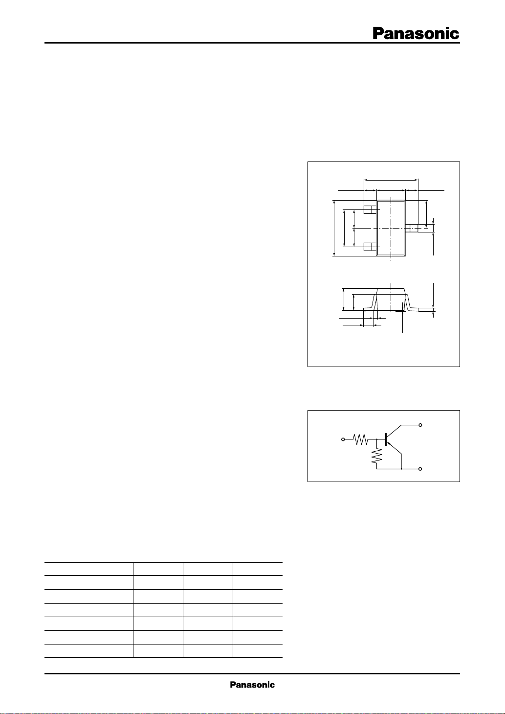
Marking Symbol (R1)(R
CBO
V
CEO
C
T
j
stg
–100 mA
–55 to +150 ˚C
)
2
1:Base
2:Emitter EIAJ:SC-59
3:Collector Mini Type Package
Internal Connection
–50 V
–50 V
200 mW
150 ˚C
Note)The part numbers in the parenthesis show conventional part number.
Unit: mm
1
Page 2

UNR2111/2112/2113/2114/2115/2116/2117/2118/2119/2110/
Transistors with built-in Resistor
Electrical Characteristics (Ta=25˚C)
■
Parameter Symbol Conditions min typ max Unit
I
Collector cutoff current
UNR211 1 – 0.5
UNR2112/2114/211E/211D/211M/211N/211T
UNR2113 – 0.1
Emitter
cutoff
current
UNR2115/2116/2117/2110 – 0.01
UNR211F/211H
UNR2119 –1.5
UNR2118/211L/211V –2.0
UNR211Z – 0.4
Collector to base voltage V
Collector to emitter voltage V
UNR211 1 35
UNR2112/211E 60
UNR2113/2114/211M 80
Forward
current
transfer
ratio
UNR2115*/2116*/2117*/2110*
UNR2119/211F/211D/211H h
UNR2118/211L 20
UNR211N/211T 80 400
UNR211V 6 20
UNR211Z 60 200
Collector to emitter saturation voltage
UNR211V IC = –10mA, IB = –1.5mA – 0.07 – 0.25 V
Output voltage high level V
Output voltage low level VCC = –5V, VB = –2.5V, RL = 1kΩ – 0.2
UNR2113
UNR211D VCC = –5V, VB = –10V, RL = 1kΩ – 0.2
UNR211E VCC = –5V, VB = –6V, RL = 1kΩ – 0.2
Transition frequency f
UNR2111/2114/2115 10
UNR2112/2117/211T 22
Input
resistance
UNR2113/2110/211D/211E 47
UNR2116/211F/21 1L/211N/211Z
UNR2118 0.51
UNR2119 1
UNR211H/211M/211V 2.2
I
I
V
V
R
CBO
CEO
EBO
T
CBO
CEO
FE
CE(sat)
OH
OL
1
211D/211E/211F/211H/211L/211M/211N/211T/211V/211Z
VCB = –50V, IE = 0 – 0.1 µA
VCE = –50V, IB = 0 – 0.5 µA
VEB = –6V, IC = 0
IC = –10mA, IE = 0 –50 V
IC = –2mA, IB = 0 –50 V
160 460
VCE = –10V, IC = –5mA 30
IC = –10mA, IB = – 0.3mA – 0.25 V
VCC = –5V, VB = – 0.5V, RL = 1kΩ –4.9 V
VCC = –5V, VB = –3.5V, RL = 1kΩ – 0.2
VCB = –10V, IE = 1mA, f = 200MHz 80 MHz
(–30%) 4.7 (+30%) kΩ
– 0.2
–1.0
mA
V
* hFE rank classification (UNR2115/2116/2117/2110)
Rank Q R S
h
FE
160 to 260 210 to 340 290 to 460
2
Page 3
UNR2111/2112/2113/2114/2115/2116/2117/2118/2119/2110/
Transistors with built-in Resistor
Electrical Characteristics (continued) (Ta=25˚C)
■
Parameter Symbol Conditions min typ max Unit
UNR2111/2112/2113/211L 0.8 1.0 1.2
UNR2114 0.17 0.21 0.25
UNR2118/2119 0.08 0.1 0.12
UNR211D 4.7
Resistance
ratio
UNR211E 2.14
UNR211F/211T R1/R
UNR211H 0.17 0.22 0.27
UNR211M 0.047
UNR211N 0.1
UNR211V 1.0
UNR211Z 0.21
211D/211E/211F/211H/211L/211M/211N/211T/211V/211Z
2
0.47
3
Page 4

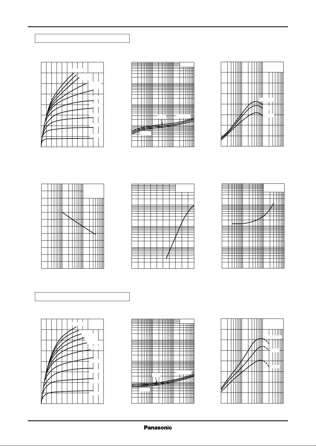
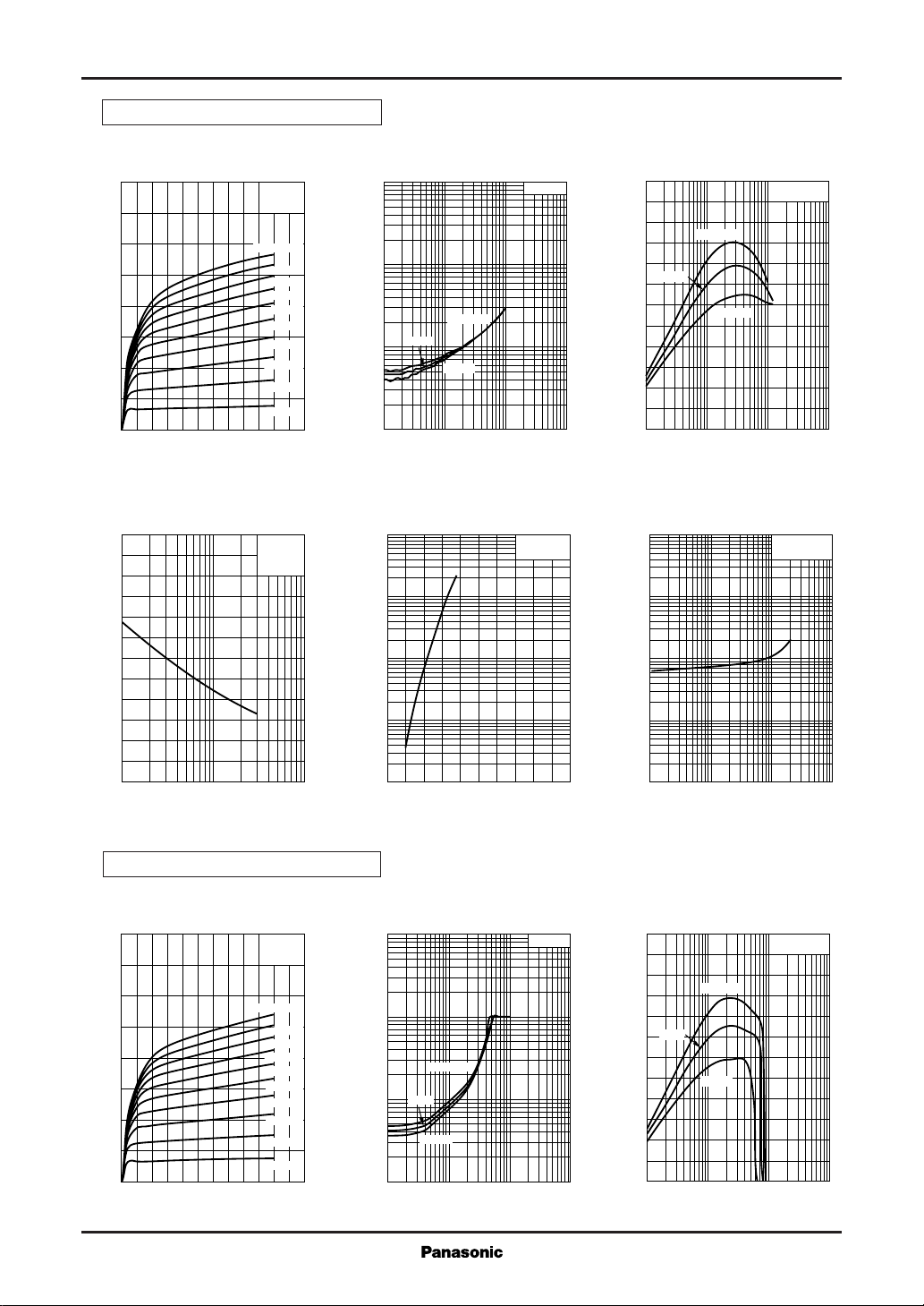
Transistors with built-in Resistor
Common characteristics chart
— Ta
P
T
250
)
200
mW
(
T
150
100
50
Total power dissipation P
0
02040 8060 140120100 160
Ambient temperature Ta (˚C
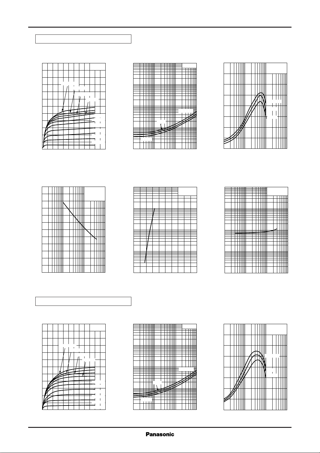
Characteristics charts of UNR2111
)
UNR2111/2112/2113/2114/2115/2116/2117/2118/2119/2110/
211D/211E/211F/211H/211L/211M/211N/211T/211V/211Z
— V
I
C
–160
–140
)
–120
mA
(
C
–100
–80
–60
–40
Collector current I
–20
0
0 –12–2 –10–4 –8–6
Collector to emitter voltage VCE (V
Cob — V
6
)
pF
(
5
ob
4
3
CE
IB=–1.0mA
CB
–0.9mA
f=1MHz
I
E
Ta=25˚C
Ta=25˚C
–0.8mA
–0.7mA
–0.6mA
–0.5mA
–0.4mA
–0.3mA
–0.2mA
–0.1mA
=0
V
— I
CE(sat)
–100
)
V
(
–30
CE(sat)
–10
–3
–1
–0.3
–0.1
–0.03
Collector to emitter saturation voltage V
–0.01
–0.1 –0.3
)
25˚C
–25˚C
–1 –3 –10 –30 –100
Collector current IC (mA
IO — V
–10000
–3000
)
–1000
µA
(
O
–300
–100
C
IC/IB=10
Ta=75˚C
160
FE
120
80
40
Forward current transfer ratio h
0
–1 –3
)
IN
)
V
(
IN
–100
–30
–10
–3
–1
VO=–5V
Ta=25˚C
hFE — I
C
VCE=–10V
–10 –30 –100 –300 –1000
Collector current IC (mA
VIN — I
O
Ta=75˚C
25˚C
–25˚C
)
VO=–0.2V
Ta=25˚C
2
1
Collector output capacitance C
0
–0.1 –0.3
–1 –3 –10 –30 –100
Collector to base voltage VCB (V
4
–30
–10
Output current I
–
3
–1
–0.4
)
Input voltage VIN (V
–1.4–1.2–1.0–0.8–0.6
)
–0.3
Input voltage V
–0.1
–0.03
–0.01
–0.1 –0.3
Output current IO (mA
–1 –3 –10 –30 –100
)
Page 5
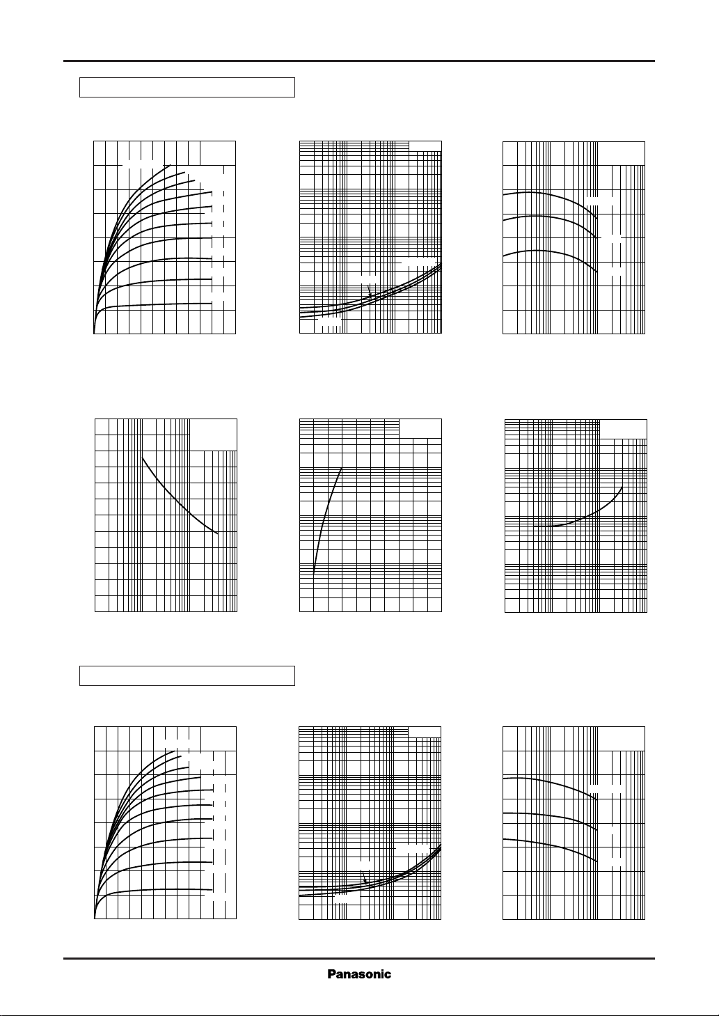
Transistors with built-in Resistor
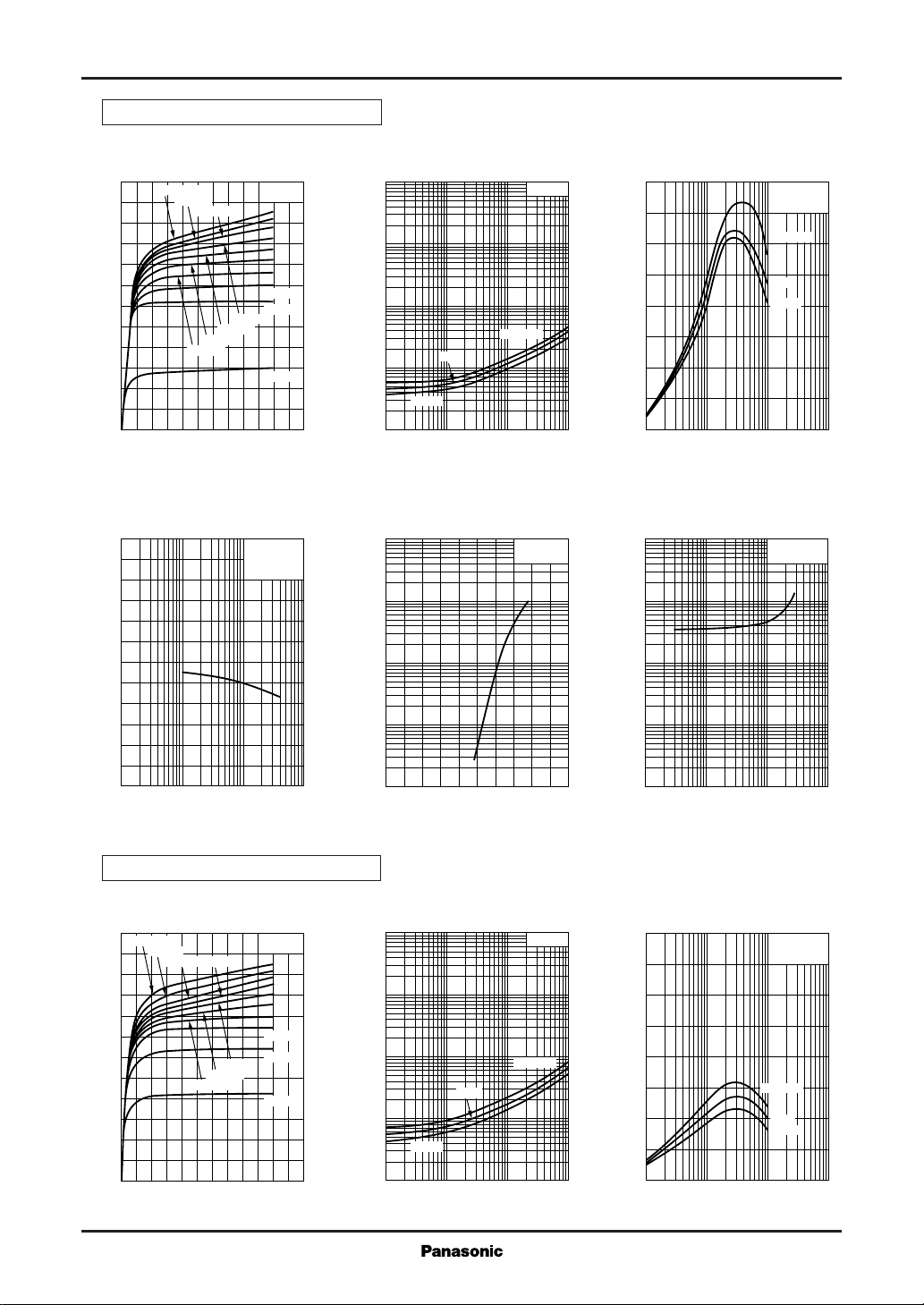
Characteristics charts of UNR2112
UNR2111/2112/2113/2114/2115/2116/2117/2118/2119/2110/
211D/211E/211F/211H/211L/211M/211N/211T/211V/211Z
— V
I
C
–160
–140
)
–120
mA
(
C
–100
–80
–60
–40
Collector current I
–20
0
0 –12–2 –10–4 –8–6
Collector to emitter voltage VCE (V
Cob — V
6
)
pF
(
5
ob
4
3
CE
IB=–1.0mA
–0.9mA
CB
–0.8mA
f=1MHz
I
E
Ta=25˚C
Ta=25˚C
–0.7mA
–0.6mA
–0.5mA
–0.4mA
–0.3mA
–0.2mA
–0.1mA
=0
V
— I
CE(sat)
–100
)
V
(
–30
CE(sat)
–10
–3
–1
–0.3
–0.1
–0.03
Collector to emitter saturation voltage V
–0.01
)
–25˚C
–0.1 –0.3
–1 –3 –10 –30 –100
Collector current IC (mA
IO — V
–10000
–3000
)
–1000
µA
(
O
–300
–100
25˚C
C
IC/IB=10
Ta=75˚C
400
FE
300
200
100
Forward current transfer ratio h
0
–1 –3
)
IN
)
V
(
IN
–100
–30
–10
–3
–1
VO=–5V
Ta=25˚C
hFE — I
C
VCE=–10V
Ta=75˚C
25˚C
–25˚C
–10 –30 –100 –300 –1000
Collector current IC (mA
VIN — I
O
VO=–0.2V
Ta=25˚C
)
2
1
Collector output capacitance C
0
–0.1 –0.3
–1 –3 –10 –30 –100
Collector to base voltage VCB (V
Characteristics charts of UNR2113
— V
I
C
–160
–140
)
–120
mA
(
C
–100
–80
–60
–40
Collector current I
–20
0
0 –12–2 –10–4 –8–6
Collector to emitter voltage VCE (V
CE
IB=–1.0mA
–0.9mA
–0.8mA
–0.7mA
Ta=25˚C
–0.6mA
–0.5mA
–0.4mA
–0.3mA
–0.2mA
–0.1mA
)
–30
–10
Output current I
–3
–1
–0.4
)
–100
)
V
(
CE(sat)
–0.3
–0.1
–0.03
Collector to emitter saturation voltage V
–0.01
Input voltage VIN (V
–30
–10
–3
–1
–25˚C
–0.1 –0.3
V
— I
CE(sat)
25˚C
–1 –3 –10 –30 –100
Collector current IC (mA
–1.4–1.2–1.0–0.8–0.6
)
C
IC/IB=10
Ta=75˚C
)
–0.3
Input voltage V
–0.1
–0.03
–0.01
–0.1 –0.3
–1 –3 –10 –30 –100
Output current IO (mA
hFE — I
400
FE
300
200
100
C
VCE=–10V
Forward current transfer ratio h
0
–1 –3
–10 –30 –100 –300 –1000
Collector current IC (mA
)
Ta=75˚C
25˚C
–25˚C
)
5
Page 6

Transistors with built-in Resistor
UNR2111/2112/2113/2114/2115/2116/2117/2118/2119/2110/
211D/211E/211F/211H/211L/211M/211N/211T/211V/211Z
)
pF
(
Cob — V
6
5
ob
4
3
2
1
CB
f=1MHz
I
=0
E
Ta=25˚C
Collector output capacitance C
0
–0.1 –0.3
–1 –3 –10 –30 –100
Collector to base voltage VCB (V
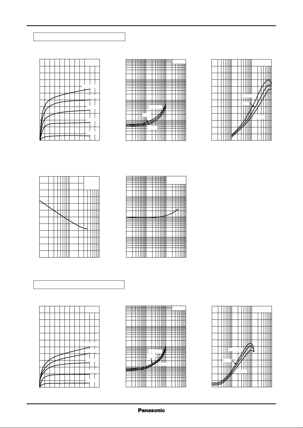
Characteristics charts of UNR2114
— V
I
C
CE
–160
–140
)
–120
mA
(
C
–100
–80
–60
–40
Collector current I
–20
0
IB=–1.0mA
0 –12–2 –10–4 –8–6
Collector to emitter voltage VCE (V
–0.9mA
–0.8mA
Ta=25˚C
–0.7mA
–0.6mA
–0.5mA
–0.4mA
–0.3mA
–0.2mA
–0.1mA
)
IO — V
IN
–10000
–3000
)
–1000
µA
(
O
–300
–100
–30
–10
Output current I
–3
–1
–0.4
)
–100
)
V
(
CE(sat)
–0.03
Collector to emitter saturation voltage V
–0.01
Input voltage VIN (V
–30
–10
–3
–1
–0.3
–0.1
–25˚C
–0.1 –0.3
V
CE(sat)
25˚C
–1 –3 –10 –30 –100
Collector current IC (mA
— I
VO=–5V
Ta=25˚C
C
Ta=75˚C
–1.4–1.2–1.0–0.8–0.6
)
IC/IB=10
)
–100
–30
)
–10
V
(
IN
–3
–1
–0.3
Input voltage V
–0.1
–0.03
–0.01
–0.1 –0.3
400
FE
300
200
100
Forward current transfer ratio h
0
–1 –3
VIN — I
O
VO=–0.2V
Ta=25˚C
–1 –3 –10 –30 –100
Output current IO (mA
hFE — I
C
VCE=–10V
Ta=75˚C
25˚C
–25˚C
–10 –30 –100 –300 –1000
Collector current IC (mA
)
)
)
pF
(
Cob — V
6
5
ob
4
3
2
1
CB
Collector output capacitance C
0
–0.1 –0.3
–1 –3 –10 –30 –100
Collector to base voltage VCB (V
6
f=1MHz
=0
I
E
Ta=25˚C
IO — V
IN
–10000
–3000
)
–1000
µA
(
O
–300
–100
–30
–10
Output current I
–3
–1
–0.4
)
Input voltage VIN (V
VO=–5V
Ta=25˚C
)
–1.4–1.2–1.0–0.8–0.6
–1000
–300
)
–100
V
(
IN
–30
–10
–3
Input voltage V
–1
–0.3
–0.1
–0.1 –0.3
VIN — I
O
VO=–0.2V
Ta=25˚C
–1 –3 –10 –30 –100
Output current IO (mA
)
Page 7
Transistors with built-in Resistor
Characteristics charts of UNR2115
UNR2111/2112/2113/2114/2115/2116/2117/2118/2119/2110/
211D/211E/211F/211H/211L/211M/211N/211T/211V/211Z
— V
I
C
CE
–160
–140
)
–120
mA
(
C
–100
–80
–60
–40
Collector current I
–20
IB=–1.0mA
0
0 –12–2 –10–4 –8–6
–0.9mA
–0.8mA
Collector to emitter voltage VCE (V
Cob — V
6
)
pF
(
5
ob
4
3
CB
f=1MHz
I
E
Ta=25˚C
Ta=25˚C
–0.7mA
–0.6mA
–0.5mA
–0.4mA
–0.3mA
–0.2mA
–0.1mA
=0
V
— I
CE(sat)
–100
)
V
(
–30
CE(sat)
–10
–3
–1
–0.3
–0.1
–0.03
Collector to emitter saturation voltage V
)
–25˚C
–0.01
–0.1 –0.3
Collector current IC (mA
25˚C
–1 –3 –10 –30 –100
IO — V
–10000
–3000
)
–1000
µA
(
O
–300
–100
C
Ta=75˚C
IC/IB=10
400
FE
300
200
100
hFE — I
C
VCE=–10V
Ta=75˚C
25˚C
–25˚C
Forward current transfer ratio h
0
–1 –3
)
IN
)
V
(
IN
–100
–30
–10
–3
–1
VO=–5V
Ta=25˚C
–10 –30 –100 –300 –1000
Collector current IC (mA
VIN — I
O
VO=–0.2V
Ta=25˚C
)
2
1
Collector output capacitance C
0
–0.1 –0.3
–1 –3 –10 –30 –100
Collector to base voltage VCB (V
Characteristics charts of UNR2116
— V
I
C
–160
–140
)
–120
mA
(
C
–100
–80
–60
–40
Collector current I
–20
0
0 –12–2 –10–4 –8–6
Collector to emitter voltage VCE (V
CE
IB=–1.0mA
–0.9mA
–0.8mA
Ta=25˚C
–0.7mA
–0.6mA
–0.5mA
–0.4mA
–0.3mA
–0.2mA
–0.1mA
)
–30
–10
Output current I
–3
–1
–0.4
)
–100
)
V
(
CE(sat)
–0.3
–0.1
–0.03
Collector to emitter saturation voltage V
–0.01
Input voltage VIN (V
–30
–10
–3
–1
–0.1 –0.3
V
— I
CE(sat)
25˚C
–25˚C
–1 –3 –10 –30 –100
Collector current IC (mA
–1.4–1.2–1.0–0.8–0.6
)
C
IC/IB=10
Ta=75˚C
)
–0.3
Input voltage V
–0.1
–0.03
–0.01
–0.1 –0.3
–1 –3 –10 –30 –100
Output current IO (mA
hFE — I
400
FE
300
200
100
C
VCE=–10V
Ta=75˚C
25˚C
–25˚C
Forward current transfer ratio h
0
–1 –3
–10 –30 –100 –300 –1000
Collector current IC (mA
)
)
7
Page 8

Transistors with built-in Resistor
UNR2111/2112/2113/2114/2115/2116/2117/2118/2119/2110/
211D/211E/211F/211H/211L/211M/211N/211T/211V/211Z
Cob — V
6
)
pF
(
5
ob
4
3
2
1
CB
f=1MHz
I
=0
E
Ta=25˚C
Collector output capacitance C
0
–0.1 –0.3
–1 –3 –10 –30 –100
Collector to base voltage VCB (V
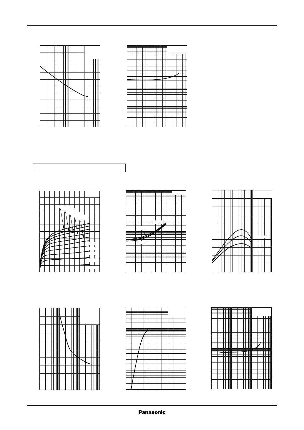
Characteristics charts of UNR2117
— V
I
C
CE
–120
–100
)
mA
(
C
–80
–60
IB=–1.0mA
–0.9mA
–0.8mA
–0.7mA
–0.6mA
–0.5mA
–0.4mA
Ta=25˚C
IO — V
IN
–10000
–3000
)
–1000
µA
(
O
–300
–100
–30
–10
Output current I
–3
–1
–0.4
)
–100
)
V
(
CE(sat)
Input voltage VIN (V
–30
–10
–3
–1
V
CE(sat)
— I
C
VO=–5V
Ta=25˚C
)
IC/IB=10
Ta=75˚C
–1.4–1.2–1.0–0.8–0.6
–100
–30
)
–10
V
(
IN
–3
–1
–0.3
Input voltage V
–0.1
–0.03
–0.01
–0.1 –0.3
400
FE
300
200
VIN — I
O
VO=–0.2V
Ta=25˚C
–1 –3 –10 –30 –100
Output current IO (mA
hFE — I
C
VCE=–10V
Ta=75˚C
)
–40
Collector current I
–20
0
0 –12–2 –10–4 –8–6
Collector to emitter voltage VCE (V
)
pF
(
Cob — V
6
5
ob
4
3
2
1
CB
Collector output capacitance C
0
–0.1 –0.3
–1 –3 –10 –30 –100
Collector to base voltage VCB (V
–0.3mA
–0.2mA
–0.1mA
f=1MHz
I
=0
E
Ta=25˚C
–0.3
–0.1
–0.03
Collector to emitter saturation voltage V
–0.01
–0.1 –0.3
)
Collector current IC (mA
–10000
–3000
)
–1000
µA
(
O
–300
–100
–30
–10
Output current I
–3
–1
–0.4
)
25˚C
–25˚C
–1 –3 –10 –30 –100
IO — V
IN
VO=–5V
Ta=25˚C
Input voltage VIN (V
25˚C
100
–25˚C
Forward current transfer ratio h
0
–1 –3
)
–100
–30
)
–10
V
(
IN
–3
–1
–0.3
Input voltage V
–0.1
–0.03
–1.4–1.2–1.0–0.8–0.6
–0.01
–0.1 –0.3
)
–10 –30 –100 –300 –1000
Collector current IC (mA
VIN — I
O
VO=–0.2V
Ta=25˚C
–1 –3 –10 –30 –100
Output current IO (mA
)
)
8
Page 9
Transistors with built-in Resistor
Characteristics charts of UNR2118
UNR2111/2112/2113/2114/2115/2116/2117/2118/2119/2110/
211D/211E/211F/211H/211L/211M/211N/211T/211V/211Z
— V
I
C
–240
–200
)
mA
(
–160
C
–120
–80
Collector current I
–40
0
0 –12–2 –10–4 –8–6
IB=–1.0mA
Collector to emitter voltage VCE (V
Cob — V
6
)
pF
(
5
ob
4
3
CE
–0.9mA
–0.8mA
CB
Ta=25˚C
–0.7mA
–0.6mA
–0.5mA
–0.4mA
–0.3mA
–0.2mA
–0.1mA
f=1MHz
I
=0
E
Ta=25˚C
V
— I
CE(sat)
–100
)
V
(
–30
CE(sat)
–10
–3
–1
–0.3
–0.1
–0.03
Collector to emitter saturation voltage V
)
–25˚C
–0.01
–0.1 –0.3
–1 –3 –10 –30 –100
Collector current IC (mA
IO — V
–10000
–3000
)
–1000
µA
(
O
–300
–100
25˚C
C
IC/IB=10
Ta=75˚C
160
FE
120
80
40
Forward current transfer ratio h
0
–1 –3
)
IN
)
V
(
IN
–100
–30
–10
–3
–1
VO=–5V
Ta=25˚C
hFE — I
C
VCE=–10V
Ta=75˚C
25˚C
–25˚C
–10 –30 –100 –300 –1000
Collector current IC (mA
VIN — I
O
VO=–0.2V
Ta=25˚C
)
2
1
Collector output capacitance C
0
–0.1 –0.3
–1 –3 –10 –30 –100
Collector to base voltage VCB (V
Characteristics charts of UNR2119
— V
I
C
–0.9mA
–0.8mA
CE
–0.7mA
Ta=25˚C
–0.6mA
–0.5mA
–0.4mA
–0.3mA
–0.2mA
–0.1mA
)
–240
–200
)
mA
(
–160
C
–120
–80
Collector current I
–40
0
IB=–1.0mA
0 –12–2 –10–4 –8–6
Collector to emitter voltage VCE (V
–30
–10
Output current I
–3
–1
)
–0.4
Input voltage VIN (V
V
— I
–100
)
V
(
–30
CE(sat)
–10
–3
–1
–0.3
–0.1
–0.03
Collector to emitter saturation voltage V
–0.01
–0.1 –0.3
CE(sat)
25˚C
–25˚C
–1 –3 –10 –30 –100
Collector current IC (mA
–1.4–1.2–1.0–0.8–0.6
)
C
IC/IB=10
Ta=75˚C
)
–0.3
Input voltage V
–0.1
–0.03
–0.01
–0.1 –0.3
–1 –3 –10 –30 –100
Output current IO (mA
hFE — I
160
FE
120
80
40
C
VCE=–10V
Ta=75˚C
25˚C
–25˚C
Forward current transfer ratio h
0
–1 –3
–10 –30 –100 –300 –1000
Collector current IC (mA
)
)
9
Page 10

Transistors with built-in Resistor
UNR2111/2112/2113/2114/2115/2116/2117/2118/2119/2110/
211D/211E/211F/211H/211L/211M/211N/211T/211V/211Z
)
pF
(
ob
Cob — V
6
5
4
3
2
1
CB
f=1MHz
I
=0
E
Ta=25˚C
Collector output capacitance C
0
–0.1 –0.3
–1 –3 –10 –30 –100
Collector to base voltage VCB (V
Characteristics charts of UNR2110
— V
I
C
CE
–120
IB=–1.0mA
–0.9mA
–100
)
mA
(
–80
C
–60
–40
Collector current I
–20
–0.8mA
–0.7mA
0
0 –12–2 –10–4 –8–6
Collector to emitter voltage VCE (V
–0.6mA
–0.5mA
–0.4mA
Ta=25˚C
–0.3mA
–0.2mA
–0.1mA
)
IO — V
IN
–10000
–3000
)
–1000
µA
(
O
–300
–100
–30
–10
Output current I
–3
–1
–0.4
)
–100
)
V
(
CE(sat)
–0.3
–0.1
–0.03
Collector to emitter saturation voltage V
–0.01
Input voltage VIN (V
–30
–10
–3
–1
–25˚C
–0.1 –0.3
V
CE(sat)
25˚C
–1 –3 –10 –30 –100
Collector current IC (mA
— I
VO=–5V
Ta=25˚C
C
Ta=75˚C
–1.4–1.2–1.0–0.8–0.6
)
IC/IB=10
)
–100
–30
)
–10
V
(
IN
–3
–1
–0.3
Input voltage V
–0.1
–0.03
–0.01
–0.1 –0.3
400
FE
300
200
100
Forward current transfer ratio h
0
–1 –3
VIN — I
O
VO=–0.2V
Ta=25˚C
–1 –3 –10 –30 –100
Output current IO (mA
hFE — I
C
VCE=–10V
Ta=75˚C
25˚C
–25˚C
–10 –30 –100 –300 –1000
Collector current IC (mA
)
)
)
pF
(
Cob — V
6
5
ob
4
3
2
1
CB
Collector output capacitance C
0
–0.1 –0.3
–1 –3 –10 –30 –100
Collector to base voltage VCB (V
10
f=1MHz
=0
I
E
Ta=25˚C
IO — V
IN
–10000
–3000
)
–1000
µA
(
O
–300
–100
–30
–10
Output current I
–3
–1
–0.4
)
Input voltage VIN (V
VO=–5V
Ta=25˚C
)
–1.4–1.2–1.0–0.8–0.6
–100
–30
)
–10
V
(
IN
–3
–1
–0.3
Input voltage V
–0.1
–0.03
–0.01
–0.1 –0.3
VIN — I
O
VO=–0.2V
Ta=25˚C
–1 –3 –10 –30 –100
Output current IO (mA
)
Page 11
Transistors with built-in Resistor
Characteristics charts of UNR211D
UNR2111/2112/2113/2114/2115/2116/2117/2118/2119/2110/
211D/211E/211F/211H/211L/211M/211N/211T/211V/211Z
— V
I
C
–60
–50
)
mA
(
–40
C
–30
–20
Collector current I
–10
IB=–1.0mA
–0.9mA
–0.4mA
0
0 –12–2 –10–4 –8–6
–0.8mA
Collector to emitter voltage VCE (V
Cob — V
6
)
pF
(
5
ob
4
3
–0.6mA
–0.5mA
CE
–0.7mA
CB
Ta=25˚C
–0.3mA
–0.2mA
–0.1mA
f=1MHz
I
=0
E
Ta=25˚C
V
— I
CE(sat)
–100
)
V
(
–30
CE(sat)
–10
–3
–1
–0.3
–0.1
–0.03
Collector to emitter saturation voltage V
–0.01
–0.1 –0.3
)
25˚C
–25˚C
–1 –3 –10 –30 –100
Collector current IC (mA
IO — V
–10000
–3000
)
–1000
µA
(
O
–300
–100
Ta=75˚C
IN
C
IC/IB=10
VO=–5V
Ta=25˚C
160
FE
120
80
40
Forward current transfer ratio h
0
–1 –3
)
–100
–30
)
–10
V
(
IN
–3
–1
hFE — I
C
VCE=–10V
Ta=75˚C
25˚C
–25˚C
–10 –30 –100 –300 –1000
Collector current IC (mA
VIN — I
O
VO=–0.2V
Ta=25˚C
)
2
1
Collector output capacitance C
0
–0.1 –0.3
–1 –3 –10 –30 –100
Collector to base voltage VCB (V
Characteristics charts of UNR211E
— V
I
C
–0.5mA
–0.4mA
CE
–0.6mA
Ta=25˚C
–0.3mA
–0.2mA
–0.1mA
)
–60
IB=–1.0mA
–0.9mA
–50
)
mA
(
–40
C
–30
–20
Collector current I
–10
0
–0.8mA –0.7mA
0 –12–2 –10–4 –8–6
Collector to emitter voltage VCE (V
–30
–10
Output current I
–3
–1
–1.5
)
–100
)
V
(
CE(sat)
–0.03
Collector to emitter saturation voltage V
–0.01
Input voltage VIN (V
–30
–10
–3
–1
–0.3
–0.1
–25˚C
–0.1 –0.3
V
— I
CE(sat)
25˚C
–1 –3 –10 –30 –100
Collector current IC (mA
–4.0–3.5–3.0–2.5–2.0
)
C
IC/IB=10
Ta=75˚C
)
–0.3
Input voltage V
–0.1
–0.03
–0.01
–0.1 –0.3
–1 –3 –10 –30 –100
Output current IO (mA
hFE — I
400
FE
300
200
100
C
Ta=75˚C
VCE=–10V
25˚C
–25˚C
Forward current transfer ratio h
0
–1 –3
–10 –30 –100 –300 –1000
Collector current IC (mA
)
)
11
Page 12

Transistors with built-in Resistor
UNR2111/2112/2113/2114/2115/2116/2117/2118/2119/2110/
211D/211E/211F/211H/211L/211M/211N/211T/211V/211Z
)
pF
(
Cob — V
6
5
ob
4
3
2
1
CB
f=1MHz
I
=0
E
Ta=25˚C
Collector output capacitance C
0
–0.1 –0.3
–1 –3 –10 –30 –100
Collector to base voltage VCB (V
Characteristics charts of UNR211F
— V
I
C
CE
–240
–200
)
mA
(
–160
C
–120
–80
Collector current I
–40
IB=–1.0mA
–0.9mA
0
0 –12–2 –10–4 –8–6
Collector to emitter voltage VCE (V
–0.8mA
–0.7mA
–0.6mA
Ta=25˚C
–0.5mA
–0.4mA
–0.3mA
–0.2mA
–0.1mA
)
IO — V
IN
–10000
–3000
)
–1000
µA
(
O
–300
–100
–30
–10
Output current I
–3
–1
–1.5
)
–100
)
V
(
CE(sat)
–0.3
–0.1
–0.03
Collector to emitter saturation voltage V
–0.01
Input voltage VIN (V
–30
–10
–3
–1
–25˚C
–0.1 –0.3
V
CE(sat)
25˚C
–1 –3 –10 –30 –100
Collector current IC (mA
— I
VO=–5V
Ta=25˚C
C
Ta=75˚C
–4.0–3.5–3.0–2.5–2.0
)
IC/IB=10
)
–100
–30
)
–10
V
(
IN
–3
–1
–0.3
Input voltage V
–0.1
–0.03
–0.01
–0.1 –0.3
160
FE
120
80
40
Forward current transfer ratio h
0
–1 –3
VIN — I
O
VO=–0.2V
Ta=25˚C
–1 –3 –10 –30 –100
Output current IO (mA
hFE — I
C
VCE=–10V
Ta=75˚C
25˚C
–25˚C
–10 –30 –100 –300 –1000
Collector current IC (mA
)
)
)
pF
(
Cob — V
6
5
ob
4
3
2
1
CB
Collector output capacitance C
0
–0.1 –0.3
–1 –3 –10 –30 –100
Collector to base voltage VCB (V
12
f=1MHz
=0
I
E
Ta=25˚C
IO — V
IN
–10000
–3000
)
–1000
µA
(
O
–300
–100
–30
–10
Output current I
–3
–1
–0.4
)
Input voltage VIN (V
VO=–5V
Ta=25˚C
)
–1.4–1.2–1.0–0.8–0.6
–100
–30
)
–10
V
(
IN
–3
–1
–0.3
Input voltage V
–0.1
–0.03
–0.01
–0.1 –0.3
VIN — I
O
VO=–0.2V
Ta=25˚C
–1 –3 –10 –30 –100
Output current IO (mA
)
Page 13
Transistors with built-in Resistor
Characteristics charts of UNR211H
UNR2111/2112/2113/2114/2115/2116/2117/2118/2119/2110/
211D/211E/211F/211H/211L/211M/211N/211T/211V/211Z
— V
I
C
–120
–100
)
mA
(
–80
C
–60
–40
Collector current I
–20
0
0 –12–2 –10–4 –8–6
Collector to emitter voltage VCE (V
Cob — V
6
)
pF
(
5
ob
4
3
CE
CB
Ta=25˚C
IB=–0.5mA
–0.4mA
–0.3mA
–0.2mA
–0.1mA
f=1MHz
I
=0
E
Ta=25˚C
V
— I
CE(sat)
–100
)
V
(
CE(sat)
–10
–1
–0.1
Collector to emitter saturation voltage V
–0.01
–1 –3
)
25˚C
–25˚C
–10 –30 –100 –300 –1000
Collector current IC (mA
VIN — I
–100
)
–10
V
(
IN
–1
Ta=75˚C
C
O
IC/IB=10
VO=–0.2V
Ta=25˚C
240
FE
200
160
120
80
40
Forward current transfer ratio h
0
–0.1 –0.3
)
hFE — I
C
VCE=–10V
Ta=75˚C
25˚C
–25˚C
–1 –3 –10 –30 –100
Collector current IC (mA
)
2
1
Collector output capacitance C
0
–3 –10 –30 –100
–1
Collector to base voltage VCB (V
Characteristics charts of UNR211L
— V
I
C
–240
–200
)
mA
(
–160
C
–120
–80
Collector current I
–40
0
0 –12–2 –10–4 –8–6
Collector to emitter voltage VCE (V
CE
Ta=25˚C
IB=–1.0mA
–0.8mA
–0.6mA
–0.4mA
–0.2mA
)
Input voltage V
–0.1
–0.01
–0.1 –0.3
)
–100
)
V
(
–30
CE(sat)
–10
–3
–1
–0.3
–0.1
–0.03
Collector to emitter saturation voltage V
–0.01
–1 –3
–1 –3 –10 –30 –100
Output current IO (mA
V
— I
CE(sat)
25˚C
–10 –30 –100 –300 –1000
C
IC/IB=10
Ta=75˚C
–25˚C
Collector current IC (mA
)
hFE — I
240
FE
200
160
120
80
40
Forward current transfer ratio h
0
–1 –3
)
Ta=75˚C
25˚C
Collector current IC (mA
C
VCE=–10V
–25˚C
–10 –30 –100 –300 –1000
)
13
Page 14
Transistors with built-in Resistor
UNR2111/2112/2113/2114/2115/2116/2117/2118/2119/2110/
211D/211E/211F/211H/211L/211M/211N/211T/211V/211Z
)
pF
(
Cob — V
6
5
ob
4
3
2
1
CB
f=1MHz
I
=0
E
Ta=25˚C
Collector output capacitance C
0
–3 –10 –30 –100
–1
Collector to base voltage VCB (V
Characteristics charts of UNR211M
— V
I
C
CE
240
200
)
mA
(
160
C
120
80
Collector current I
40
0
0 –12–2 –10–4 –8–6
IB=–1.0mA
–0.9mA
Collector to emitter voltage VCE (V
–0.8mA
–0.7mA
Ta=25˚C
–0.6mA
–0.5mA
–0.4mA
–0.3mA
–0.2mA
–0.1mA
)
VIN — I
–100
)
–10
V
(
IN
–1
Input voltage V
–0.1
–0.01
–0.1 –0.3
)
)
V
(
CE(sat)
–0.03
–0.01
–0.003
Collector to emitter saturation voltage V
–0.001
Output current IO (mA
V
CE(sat)
–10
–3
–1
–0.3
–1 –3
25˚C
–25˚C
–10 –30 –100 –300 –1000
–0.1
Collector current IC (mA
O
VO=–0.2V
Ta=25˚C
–1 –3 –10 –30 –100
)
— I
C
IC/IB=10
Ta=75˚C
)
hFE — I
C
500
FE
400
300
200
100
VCE=–10V
Ta=75˚C
25˚C
–25˚C
Forward current transfer ratio h
0
–1 –3
–10 –30 –100 –300 –1000
Collector current IC (mA
)
)
pF
(
Cob — V
10
8
ob
6
4
2
CB
Collector output capacitance C
0
–0.1 –0.3
–1 –3 –10 –30 –100
Collector to base voltage VCB (V
14
f=1MHz
I
=0
E
Ta=25˚C
)
–4
10
)
–3
10
µA
(
O
–2
10
–1
10
Output current I
1
–0.4
Input voltage VIN (V
IO — V
IN
VO=–5V
Ta=25˚C
–1.4–1.2–1.0–0.8–0.6
–100
–30
)
–10
V
(
IN
–3
–1
–0.3
Input voltage V
–0.1
–0.03
–0.01
–0.1 –0.3
)
VIN — I
O
VO=–0.2V
Ta=25˚C
–1 –3 –10 –30 –100
Output current IO (mA
)
Page 15
Transistors with built-in Resistor
Characteristics charts of UNR211N
UNR2111/2112/2113/2114/2115/2116/2117/2118/2119/2110/
211D/211E/211F/211H/211L/211M/211N/211T/211V/211Z
— V
I
C
–200
–175
)
–150
mA
(
C
–125
–100
–75
–50
Collector current I
–25
0
0 –12–2 –10–4 –8–6
Collector to emitter voltage VCE (V
Cob — V
6
)
pF
(
5
ob
4
3
CE
CB
Ta=25˚C
IB=–1.0mA
–0.9mA
–0.8mA
–0.7mA
–0.6mA
–0.5mA
–0.4mA
–0.3mA
–0.2mA
–0.1mA
f=1MHz
=0
I
E
Ta=25˚C
V
— I
CE(sat)
–10
)
V
(
CE(sat)
–1
Ta=75˚C
25˚C
–0.1
–25˚C
Collector to emitter saturation voltage V
–0.01
–1
)
–10 –100 –1000
Collector current IC (mA
IO — V
–10000
)
–1000
µA
(
O
–100
C
IC/IB=10
300
FE
250
200
150
100
50
Forward current transfer ratio h
0
–1
)
IN
)
V
(
IN
–100
–10
–1
VO=–5V
Ta=25˚C
hFE — I
C
VCE=–10V
Ta=75˚C
25˚C
–25˚C
–10 –100 –1000
Collector current IC (mA
VIN — I
O
VO=–0.2V
Ta=25˚C
)
2
1
Collector output capacitance C
0
–1
–10 –100
Collector to base voltage VCB (V
Characteristics charts of UNR211T
— V
I
C
CE
–200
–175
)
–150
mA
(
C
–125
–100
–75
–50
Collector current I
–25
0
0 –12–2 –10–4 –8–6
Collector to emitter voltage VCE (V
Ta=25˚C
IB=–1.0mA
–0.9mA
–0.8mA
–0.7mA
–0.6mA
–0.5mA
–0.4mA
–0.3mA
–0.2mA
–0.1mA
)
–10
Output current I
–1
–0.4
)
)
V
(
CE(sat)
Collector to emitter saturation voltage V
–0.01
Input voltage VIN (V
–10
–1
–0.1
25˚C
–1
V
— I
CE(sat)
Ta=75˚C
–25˚C
–10 –100 –1000
C
Collector current IC (mA
–1.4–1.2–1.0–0.8–0.6
)
IC/IB=10
)
Input voltage V
–0.1
–0.01
–0.1
–1 –10 –100
Output current IO (mA
hFE — I
C
300
FE
250
200
150
100
50
Forward current transfer ratio h
0
–1
Ta=75˚C
25˚C
–25˚C
–10 –100 –1000
VCE=–10V
Collector current IC (mA
)
)
15
Page 16

Transistors with built-in Resistor
UNR2111/2112/2113/2114/2115/2116/2117/2118/2119/2110/
211D/211E/211F/211H/211L/211M/211N/211T/211V/211Z
IO — V
IN
–10000
)
–1000
µA
(
O
–100
–10
Output current I
–1
–0.4
Input voltage VIN (V
VO=–5V
Ta=25˚C
)
Characteristics charts of UNR211V
— V
I
C
CE
–12
–10
)
mA
(
–8
C
–6
–4
Collector current I
–2
0
0 –12–2 –10–4 –8–6
Collector to emitter voltage VCE (V
Ta=25˚C
IB=–1.0mA
–0.9mA
–0.8mA
–0.7mA
–0.6mA
–0.5mA
–0.4mA
–0.3mA
–0.2mA
–0.1mA
)
VIN — I
–100
)
–10
V
(
IN
–1
Input voltage V
–0.1
–1.4–1.2–1–0.8–0.6
–0.01
–0.1
Output current IO (mA
V
–10
)
V
(
CE(sat)
–1
–0.1
Collector to emitter saturation voltage V
–0.01
–1
25˚C
–10 –100 –1000
Collector current IC (mA
O
VO=–0.2V
Ta=25˚C
–1 –10 –100
)
— I
CE(sat)
C
IC/IB=10
Ta=75˚C
–25˚C
)
hFE — I
C
12
FE
Forward current transfer ratio h
Ta=75˚C
10
8
6
4
2
0
–1
–25˚C
VCE=–10V
25˚C
–10 –100
Collector current IC (mA
)
–10000
)
–1000
µA
(
O
–100
–10
Output current I
–1
–0.4
Input voltage VIN (V
16
IO — V
IN
VO=–5V
Ta=25˚C
)
VIN — I
O
–100
)
–10
V
(
IN
–1
Input voltage V
–0.1
–1.4–1.2–1–0.8–0.6
–0.01
–0.1
–1 –10 –100
Output current IO (mA
VO=–0.2V
Ta=25˚C
)
Page 17

Transistors with built-in Resistor
Characteristics charts of UNR211Z
UNR2111/2112/2113/2114/2115/2116/2117/2118/2119/2110/
211D/211E/211F/211H/211L/211M/211N/211T/211V/211Z
— V
I
C
–200
–175
)
–150
mA
(
C
–125
–100
–75
–50
Collector current I
–25
0
0 –12–2 –10–4 –8–6
Collector to emitter voltage VCE (V
Cob — V
6
)
pF
(
5
ob
4
3
CE
CB
Ta=25˚C
IB=–1.0mA
–0.9mA
–0.8mA
–0.7mA
–0.6mA
–0.5mA
–0.4mA
–0.3mA
–0.2mA
–0.1mA
f=1MHz
=0
I
E
Ta=25˚C
V
— I
CE(sat)
–10
)
V
(
CE(sat)
–1
Ta=75˚C
–0.1
25˚C
–25˚C
Collector to emitter saturation voltage V
–0.01
–1
)
–10 –100 –1000
Collector current IC (mA
IO — V
–10000
)
–1000
µA
(
O
–100
C
IC/IB=10
300
FE
250
200
150
100
50
Forward current transfer ratio h
0
–1
)
IN
)
(
V
IN
–100
–10
–1
VO=–5V
Ta=25˚C
hFE — I
C
VCE=–10V
Ta=75˚C
25˚C
–25˚C
–10 –100 –1000
Collector current IC (mA
VIN — I
O
VO=–0.2V
Ta=25˚C
)
2
1
Collector output capacitance C
0
–1
–10 –100
Collector to base voltage VCB (V
–10
Output current I
–1
–0.4
)
Input voltage VIN (V
–1.4–1.2–1–0.8–0.6
)
Input voltage V
–0.1
–0.01
–0.1
Output current IO (mA
–1 –10 –100
)
17
Page 18

Request for your special attention and precautions in using the technical information
and semiconductors described in this material
(1) An export permit needs to be obtained from the competent authorities of the Japanese Govern-
ment if any of the products or technologies described in this material and controlled under the
"Foreign Exchange and Foreign Trade Law" is to be exported or taken out of Japan.
(2) The technical information described in this material is limited to showing representative character-
istics and applied circuit examples of the products. It does not constitute the warranting of industrial
property, the granting of relative rights, or the granting of any license.
(3) The products described in this material are intended to be used for standard applications or gen-
eral electronic equipment (such as office equipment, communications equipment, measuring instruments and household appliances).
Consult our sales staff in advance for information on the following applications:
• Special applications (such as for airplanes, aerospace, automobiles, traffic control equipment,
combustion equipment, life support systems and safety devices) in which exceptional quality and
reliability are required, or if the failure or malfunction of the products may directly jeopardize life or
harm the human body.
• Any applications other than the standard applications intended.
(4) The products and product specifications described in this material are subject to change without
notice for reasons of modification and/or improvement. At the final stage of your design, purchasing, or use of the products, therefore, ask for the most up-to-date Product Standards in advance to
make sure that the latest specifications satisfy your requirements.
(5) When designing your equipment, comply with the guaranteed values, in particular those of maxi-
mum rating, the range of operating power supply voltage and heat radiation characteristics. Otherwise, we will not be liable for any defect which may arise later in your equipment.
Even when the products are used within the guaranteed values, redundant design is recommended,
so that such equipment may not violate relevant laws or regulations because of the function of our
products.
(6) When using products for which dry packing is required, observe the conditions (including shelf life
and after-unpacking standby time) agreed upon when specification sheets are individually exchanged.
(7) No part of this material may be reprinted or reproduced by any means without written permission
from our company.
Please read the following notes before using the datasheets
A. These materials are intended as a reference to assist customers with the selection of Panasonic
semiconductor products best suited to their applications.
Due to modification or other reasons, any information contained in this material, such as available
product types, technical data, and so on, is subject to change without notice.
Customers are advised to contact our semiconductor sales office and obtain the latest information
before starting precise technical research and/or purchasing activities.
B. Panasonic is endeavoring to continually improve the quality and reliability of these materials but
there is always the possibility that further rectifications will be required in the future. Therefore,
Panasonic will not assume any liability for any damages arising from any errors etc. that may appear in this material.
C. These materials are solely intended for a customer's individual use.
Therefore, without the prior written approval of Panasonic, any other use such as reproducing,
selling, or distributing this material to a third party, via the Internet or in any other way, is prohibited.
2001 MAR
 Loading...