

Page 1

DATA SH EET
Product specification
Supersedes data of October 1991
File under Integrated circuits, IC03
October 1992
INTEGRATED CIRCUITS
UMA1014
Low-power frequency synthesizer
for mobile radio communications
Page 2
October 1992 2
Philips Semiconductors Product specification
Low-power frequency synthesizer for
mobile radio communications
UMA1014
FEATURES
• Single chip synthesizer; compatible with Philips cellular
radio chipset
• Fully programmable RF divider
• I2C interface for two-line serial bus
• On-chip crystal oscillator/TCXO buffer from 3 to 16 MHz
• 16 reference division ratios allowing 5 to 100 kHz
channel spacing
• 1/8 crystal frequency output
• On-chip out-of-lock indication
• Two extra VCO control outputs
• Latched synthesizer alarm output
• Status register including out-of-lock indication and
power failure
• Power-down mode.
APPLICATIONS
• Cellular mobile radio (NMT, AMPS, TACS)
• Private mobile radio (PMR)
• Cordless telephones.
GENERAL DESCRIPTION
The UMA1014 is a low-power universal synthesizer which
has been designed for use in channelized radio
communication. The IC is manufactured in bipolar
technology and is designed to operate at 5 to 100 kHz
channel spacing with an RF input from 50 to 1100 MHz.
The channel is programmed via a standard I
2
C-bus. A
low-power sensitive RF divider is incorporated together
with a dead-zone eliminated, 3-state phase comparator.
The low-noise charge pump delivers 1 mA or 1/2 mA
output current to enable a better compromise between fast
switching and loop bandwidth. A power-down circuit
enables the synthesizer to be set to idle mode.
QUICK REFERENCE DATA
ORDERING INFORMATION
SYMBOL PARAMETER MIN. TYP. MAX. UNIT
V
CC
, V
CP
supply voltage range 4.5 5.0 5.5 V
I
CC
+ I
CP
supply current − 13 − mA
I
CCpd
ICC in power-down − 2.5 − mA
f
ref
phase comparator reference frequency 5 − 100 kHz
f
RF
RF input frequency 50 − 1100 MHz
T
amb
operating ambient temperature range −40 − 85 °C
TYPE NUMBER
PACKAGE
NAME DESCRIPTION VERSION
UMA1014T SO16 plastic small outline package; 16 leads; body width 3.9 mm SOT109-1
Page 3
October 1992 3
Philips Semiconductors Product specification
Low-power frequency synthesizer for
mobile radio communications
UMA1014
BLOCK DIAGRAM
Fig.1 Block diagram.
handbook, full pagewidth
1
2
8
11
12
15 9 10 7 13
MAIN
CONTROL
3-BITS
VCO buffer switch output B
VCO buffer switch output A
serial data input/output
serial clock input
18-BITS 4-BITS 1-BIT 1-BIT
MAIN
DIVIDER
REFERENCE
DIVIDER
PHASE
COMPARATOR
CHARGE
PUMP
OUT-OF-
LOCK
31/32
BUFFER/
OSCILLATOR
UMA1014
internally
connected
+5 V charge
pump supply
1/8 crystal
frequency
output
ground+5 V supply
4 6 16 14 3
5
charge
pump
output
oscillator input
RF input
oscillator output
hardware
power-down
slave address
select input A
synthesizer
alarm
output
MRA396 - 1
Page 4

October 1992 4
Philips Semiconductors Product specification
Low-power frequency synthesizer for
mobile radio communications
UMA1014
PINNING
SYMBOL PIN DESCRIPTION
OSCIN 1 oscillator or TCXO input
OSCOUT 2 oscillator output
V
CP
3 5 V charge pump supply
V
CC
4 5 V supply
PCD 5 charge pump output
GND 6 ground
VCOA 7 VCO buffer switch output A
(including out-of-lock)
RF 8 RF input
SCL 9 serial clock input
SDA 10 serial data input/output
HPD 11 hardware power-down (active LOW)
SAA 12 slave address select input A
VCOB 13 VCO buffer switch output B
i.c. 14 internally connected
SYA 15 synthesizer alarm output
FX8 16 1/8 crystal frequency output
Fig.2 Pin configuration.
handbook, halfpage
1
3
215
16
14
13
12
11
10
9
5
6
7
8
4
UMA1014
OSCIN
V
OSCOUT
PCD
GND
VCOA
RF
V
CP
CC
FX8
SYA
i.c.
VCOB
SDA
HPD
SAA
SCL
MRA397 - 1
Page 5

October 1992 5
Philips Semiconductors Product specification
Low-power frequency synthesizer for
mobile radio communications
UMA1014
FUNCTIONAL DESCRIPTION
The UMA1014 is a low-power frequency synthesizer for
radio communication which operates in the
50 to 1100 MHz range. The device includes an
oscillator/buffer circuit, a reference divider, an RF divider,
a 3-state phase comparator, a charge pump and a main
control circuit to transfer the serial data into the four
internal 8-bit registers. The VCC supply feeds the logic part,
the VCP supply feeds the charge-pump only. Both supplies
are +5 V (±10%). The power-down facility puts the
synthesizer in the idle mode (all current supplies are
switched off except in the control part). This allows any I
2
C
transfer and all information in the registers is retained thus
enabling fast power-up.
Main divider
The main divider is a pulse swallow type counter which is
fully programmable. After a sensitive input amplifier
(50 mV, −13 dBm), the RF signal is applied to a 31/32
duo-modulus counter. The output is then used as the clock
for the 5-bit swallow counter R = (MD4 to MD0) and the
13-bit main counter N = (MD17 to MD5). The ratio is
transferred via the I
2
C-bus to the registers B, C and D, and
then buffered in an 18-bit latch. The ratio in the divider
chain is updated with the new information when the least
significant bit is received (i.e. D0). This update is
synchronized to the output of the divider in order to limit the
phase error during small jumps of the synthesized
frequency.
The main divider can be programmed to any value
between 2048 and 262143 (i.e. 218−1). If ratio X, below
2048, is sent to the divider, the ratio (X + 2048) will be
programmed. When it is required to switch between
adjacent channels it is possible to program register D only,
thus allowing shorter I2C programming time.
Oscillator
The oscillator is a common collector Colpitts type with
external capacitive feedback. The oscillator has very small
temperature drift and high voltage supply rejection. A
TCXO or other type of clock can be used to drive the
oscillator by connecting the source (preferably
AC-coupled) to pin 1 and leaving pin 2 open-circuit. The
oscillator acts as a buffer in this mode and requires no
additional external components. The signal from the clock
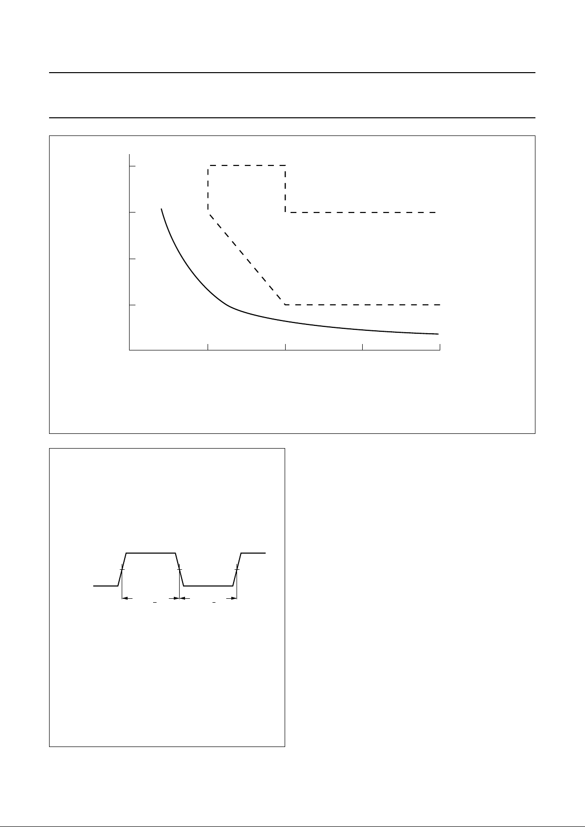
source should have a minimum space width of 31 ns.
Reference divider
The reference divider is semi-programmable with 16
division ratios which can be selected via the I
2
C-bus. The
programming uses four bits of the register A (A3 to A0) as
listed in Table 2. These ratios allow the use of a large
number of crystal frequencies from 3 MHz up to 16 MHz.
All main channel spacings can be obtained with a single
crystal/TXCO frequency of 9.6 MHz.
Phase comparator
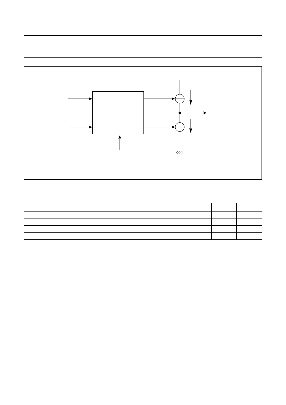
A diagram of the phase comparator and charge pump is
illustrated in Fig.3.
The phase comparator is both a phase and frequency
detector. The detector comprises dual flip-flops together
with logic circuitry to eliminate the dead-zone. When a
phase error is detected the UP or DOWN signal goes
HIGH. This switches on the corresponding current
generator which produces a source or sink current for the
loop filter. When no phase error is detected PCD goes high
impedance. The final tuning voltage for the VCO is
provided by the loop filter. The charge pump current is
programmable via the I
2
C-bus. When IPCD (bit 5) is set to
logic 1 the charge pump delivers 1 mA; when IPCD is set
to logic 0 the charge pump delivers 0.5 mA.
The phase comparator has a phase inverter logic input
(PHI). This allows the use of inverted or non-inverted loop
filter configurations. It is thus possible to use a passive
loop filter which offers higher performances without an
operational amplifier. The function of the phase
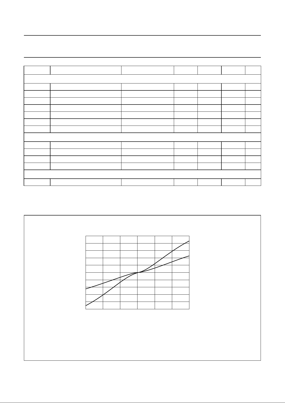
comparator is given in Table 3 and a typical transfer curve
is illustrated in Fig.4.
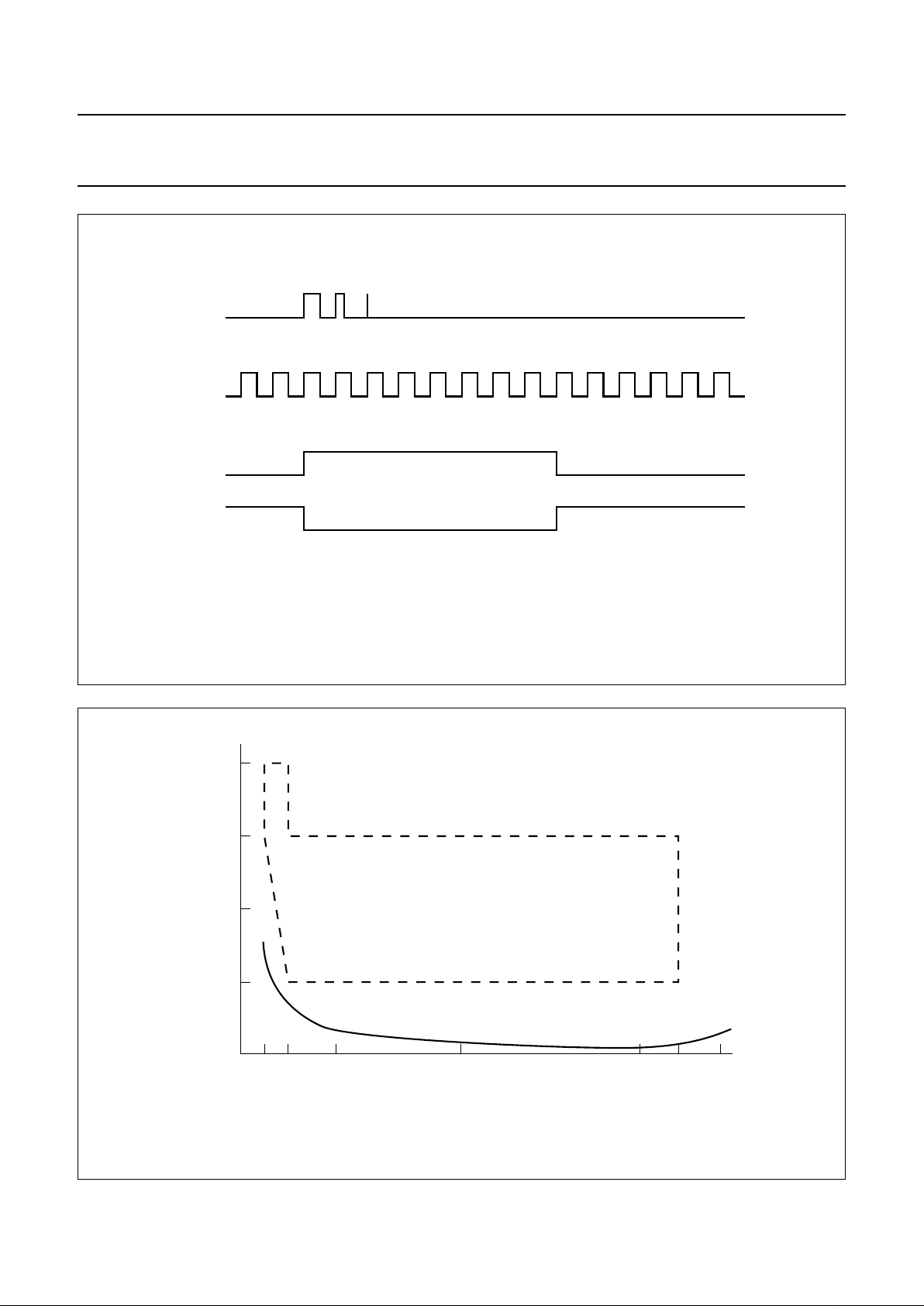
Out-of-lock detector
An out-of-lock detector using the UP and DOWN signals
from the phase comparator is included on-chip. The pin
VCOA is an open collector output which is forced LOW
during an out-of-lock condition. The same information is
also available via the I
2
C-bus in the status register (bit
OOL). When the phase error (measured at the phase
comparator) is greater than approximately 200 ns, an
out-of-lock condition is immediately flagged. The flag is
only released after 6 reference cycles when the phase
error is less than 200 ns.
Page 6
October 1992 6
Philips Semiconductors Product specification
Low-power frequency synthesizer for
mobile radio communications
UMA1014
Table 1 Division ratio in the main divider
Table 2 Reference divider programming
Table 3 Operation of the phase comparator
MAIN COUNTER: N SWALLOW COUNTER: R
MD17 MD16 MD15 ... MD8 MD7 ... MD5 MD4 ... MD0
B1 B0 C7 ... C0 D7 ... D5 D4 ... D0
MSB LSB
A3(RD3) A2(RD2) A1(RD1) A0(RD0)
REFERENCE DIVISION
RATIO
CHANNEL SPACING FOR 9.6 MHz AT
OSCIN
0000 128 75 kHz
0001 160 60 kHz
0010 192 50 kHz
0011 240 40 kHz
0100 256 37.5 kHz
0101 320 30 kHz
0110 384 25 kHz
0111 480 20 kHz
1000 512 18.75 kHz
1001 640 15 kHz
1010 768 12.5 kHz
1011 960 10 kHz
1100 1024 9.375 kHz
1101 1280 7.5 kHz
1110 1536 6.25 kHz
1111 1920 5 kHz
PHI = 0 (PASSIVE LOOP FILTER) PHI = 1 (ACTIVE LOOP FILTER)
f
ref
< f
var
f
ref
> f
var
f
ref
= f
var
f
ref
< f
var
f
ref
> f
var
f
ref
= f
var
UP010100
DOWN 100010
I
pcd
−1 mA 1 mA <±5 nA 1 mA −1 mA <±5 nA
Page 7
October 1992 7
Philips Semiconductors Product specification
Low-power frequency synthesizer for
mobile radio communications
UMA1014
MAIN CONTROL
The control part consists mainly of the I2C-bus control
interface and a set of four registers A, B, C and D. The
serial input data (SDA) is converted into 8-bit parallel
words and stored in the appropriate registers. The data
transmission to the synthesizer is executed in the burst
mode with the following format:
//slave addr./subaddr./data1/data2/.../datan//; n up to 4
Data byte 1 is written in the register indicated by the
subaddress. An auto-increment circuit, if enabled
(AVI = 1), then provides the correct addressing for the
ensuing data bytes. Since the length of the data burst is
not fixed, it is possible to program only one register or the
whole set. The registers are structured in such a way so
that the burst, for normal operation, is kept as short as
possible. The bits that are only programmed during the
set-up (reference division ratio, power-down, phase
inversion and current on PCD) are stored in registers A
and B.
In the slave address six bits are fixed, the remaining two
bits depend on the application.
Table 4 Slave address
110001
SAA R/W
SAA is the slave address. When SAA goes HIGH then
SAA = 0, when SAA goes LOW then SAA = 1. This allows
the use of two UMA1014s on the same bus but using a
different address. R/W should be set to logic 0 when
writing to the synthesizer or set to logic 1 when reading the
status register.
The subaddress includes the register pointer, and sets the
two flags related to the auto-increment (AVI) and the alarm
disable (DI).
Table 5 Subaddress
X X X DI AVI X SB1 SB0
Where:
X = not used
DI (Disable Interrupt):
DI = 1 disables the alarm on SYA
DI = 0 enables the alarm.
AVI (Auto Value Increment):
AVI = 1 enables the automatic increment
AVI = 0 disables the auto-increment.
SB1/SB0 are the pointers of the register where DATA1 will
be written (see Table 6).
When the auto-increment is disabled (AVI = 0), the
subaddress pointer will maintain the same value during the
I2C-bus transfer. All the data bytes will then be written
consecutively in the register pointed by the subaddress.
Table 6 Pointer of the registers
SB1 SB0 REGISTER POINTED
00 A
01 B
10 C
11 D
Page 8
October 1992 8
Philips Semiconductors Product specification
Low-power frequency synthesizer for
mobile radio communications
UMA1014
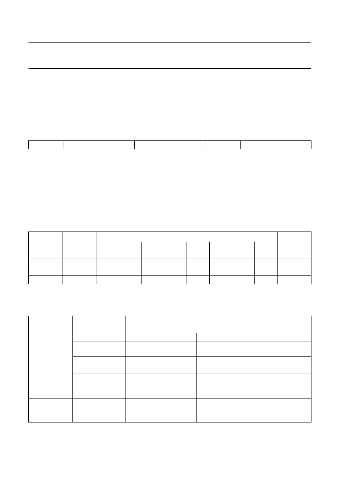
Status register and synthesizer alarm
When an out-of-lock condition or a power dip occurs,
SYA, which is an open collector output, is forced LOW
and latched. The pin SYA will be released after the status
register is read via the I2C-bus.
The status register contains the following information:
Table 7 Status register
Where:
OOL = momentary out-of-lock
LOOL = latched out-of-lock
LPD = latched power dip
DI = disable interrupt (of the last write cycle).
The I
2
C-bus protocol to read this internal register is a single byte without subaddressing:
//slave address (R/W = 1)/status register (read)//
Table 8 Bit allocation
Where X = not used
Table 9 Register allocation
0 0 0 OOL 0 LOOL LPD DI
REGISTER POINTER BIT ALLOCATION PRESET
76543210
A 00 PD X IPCD X RD3 RD2 RD1 RD0 00001110
B 01 1 0 1 PHI VCOB VCOA MD17 MD16 10100101
C 10 MD15 MD14 MD13 MD12 MD11 MD10 MD9 MD8 00111000
D 11 MD7 MD6 MD5 MD4 MD3 MD2 MD1 MD0 10000000
REGISTER
NAME
BIT NAME FUNCTION
PRESET
VALUE
A PD power down PD = 0 normal operation 0
IPCD programmable charge
pump current
IPCD = 1=1mA;
IPCD = 0 = 0.5 mA
0
RD3...RD0 reference ratio see Table 2 1110; r = 1536
B PHI phase inverter PHI = 0 passive loop filter 0
VCOA VCO switch A set pin 7 1
VCOB VCO switch B set pin 13 0
MD17, MD16 bits 17 and 16 MSB of main divider ratio 01
C MD15 to MD8 bits 15 to 8 main divider ratio 00111000
D MD7 to MD0 bits 7 to 0 main divider ratio 10000000;
r = 80000
Page 9
October 1992 9
Philips Semiconductors Product specification
Low-power frequency synthesizer for
mobile radio communications
UMA1014
LIMITING VALUES
In accordance with the Absolute Maximum System (IEC 134).
HANDLING
Every pin referenced to ground withstands ESD (HMB) tests in accordance with MIL-STD-883C method 3015 class 2.
Inputs and outputs are protected against electrostatic discharges in normal handling. However, to be totally safe, it is
desirable to take normal precautions appropriate to handling Integrated Circuits.
SYMBOL PARAMETER MIN. MAX. UNIT
V
CC
supply voltage range −0.3 7.0 V
V
i
voltage range to ground (all pins) 0 V
CC
V
T
stg
IC storage temperature range −55 +125 °C
T
amb
operating ambient temperature range −40 +85 °C
Fig.3 Phase comparator block diagram.
handbook, full pagewidth
PHASE
COMPARATOR
DOWN
UP
f
var
f
ref
PHI
on/off
on/off
V
CP
1 mA
(source)
1 mA
(sink)
PCD
MRA399
Page 10
October 1992 10
Philips Semiconductors Product specification
Low-power frequency synthesizer for
mobile radio communications
UMA1014
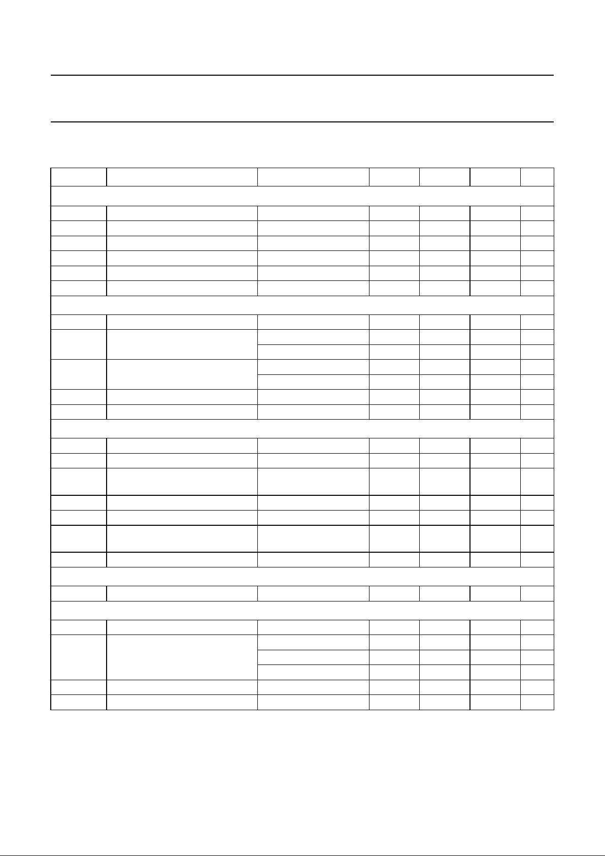
CHARACTERISTICS
T
amb
= 25 °C; VCC = 4.5 to 5.5 V; unless otherwise specified.
SYMBOL PARAMETER CONDITIONS MIN. TYP. MAX. UNIT
Supply (pins V
CC
and VCP)
V
CC
supply voltage range 4.5 − 5.5 V
I
CC
supply current − 11.5 13.5 mA
I
CCpd
supply current power-down − 2.5 3.3 mA
V
CP
charge pump supply voltage 4.5 − 5.5 V
I
CP
charge pump supply current IPCD = 0.5 mA − 1.4 1.8 mA
I
CPpd
charge pump supply current power-down − 0.01 − mA
RF dividers (pin RF)
f
RF
frequency range 50 − 1100 MHz
V
RF(rms)
input voltage level (RMS value) 50 to 100 MHz 150 − 200 mV
100 to 1100 MHz 50 − 150 mV
R
I
input resistance at 1 GHz − 200 −Ω
at 100 MHz − 600 −Ω
C
I
input capacitance note 1 − 2.0 − pF
R
RF
division ratios 2048 − 262143 −
Oscillator and reference divider (pins OSCIN and OSCOUT)
f
OSC
oscillator frequency range 3 − 16 MHz
V
OSC(RMS)
input level sine wave (RMS value) 0.15 − VCC/2.8 V
V
OSC(p-p)
input level square wave
(peak-to-peak value)
0.45 − V
CC
V
t
OSC_mk
input mark width see Fig.8 10 −−ns
t
OSC_sp
input space width 31 −−ns
Z
OSC
output impedance at pin
OSCOUT
−−2kΩ
R
ref
reference division ratio see Table 1 128 − 1920
1/8 crystal frequency (open collector output) (pin FX8)
I
OL
LOW level output current VOL≥ 0.6 V 1.0 −−mA
Phase comparator (pin PCD)
f
PCD
frequency range 5 − 100 kHz
I
PCD
output current V
PCD
= 2.5 V
bit IPCD = 1 0.9 1.2 1.4 mA
bit IPCD = 0 0.45 0.6 0.75 mA
I
PCDL
output leakage current −5 ±1+5nA
V
PCD
output voltage 0.4 − VCP−0.5 V
Page 11
October 1992 11
Philips Semiconductors Product specification
Low-power frequency synthesizer for
mobile radio communications
UMA1014
Notes
1. CI is in parallel with RI.
2. Pin VCOA is forced to logic 0 during out-of-lock condition.
Serial clock and serial data input (pins SCL and SDA)
f
CLK
clock frequency 0 − 100 kHz
V
IH
HIGH level input voltage 3 −−V
V
IL
LOW level input voltage −−1.5 V
I
IH
HIGH level input current − 310µA
I
IL
LOW level input current −10 −5 −µA
C
I
input capacitance −−10 pF
I
sink
SDA sink current VOL = 0.4 V 3 −−mA
Slave address select input (pin SAA) and Hardware power-down input (pin HPDN)
V
IH
HIGH level input voltage 3 −−V
V
IL
LOW level input voltage −−0.4 V
I
IH
HIGH level input current −−0.1 µA
I
IL
LOW level input current −10 −−µA
VCO output switches (pins VCOA and VCOB) and synthesizer alarm (pin SYA); note2
I
OL
LOW level sink current VOL≥ 0.4 V 400 −−µA
SYMBOL PARAMETER CONDITIONS MIN. TYP. MAX. UNIT
Fig.4 Gain of phase detector and charge pump.
The current I
PCD
is averaged over a reference period of 24 µs.
2.0
1.0
0
-1.0
-2.0
-20 0 20
I = 1 mA
PCD
I = 0.5 mA
PCD
phase difference (t = ns)
I
(µA)
MRA400
Page 12
October 1992 12
Philips Semiconductors Product specification
Low-power frequency synthesizer for
mobile radio communications
UMA1014
Fig.5 Out-of-lock function.
UP or DOWN
REF
OOL
VCOA
MRA401
Fig.6 RF input high frequency sensitivity.
200
100
50 100 200 500
1000
1100
1200
guaranteed area
of operation
RF input
(mV RMS)
f (MHz)
RF
typical RF
sensitivity
(T = 25 C)
amb
o
MRA402 - 1
0
Page 13
October 1992 13
Philips Semiconductors Product specification
Low-power frequency synthesizer for
mobile radio communications
UMA1014
Fig.7 RF input low frequency sensitivity.
guaranteed area
of operation
50
RF input
(mV RMS)
0
100
50
200
typical RF
sensitivity
(T = 25 C)
amb
o
f (MHz)
RF
MRA403 - 1
200
150
100
150
Fig.8 Oscillator input timing.
handbook, halfpage
OSCIN
t
OSC mk
OSC sp
t
MLA436 - 1
Page 14
October 1992 14
Philips Semiconductors Product specification
Low-power frequency synthesizer for
mobile radio communications
UMA1014
APPLICATION INFORMATION
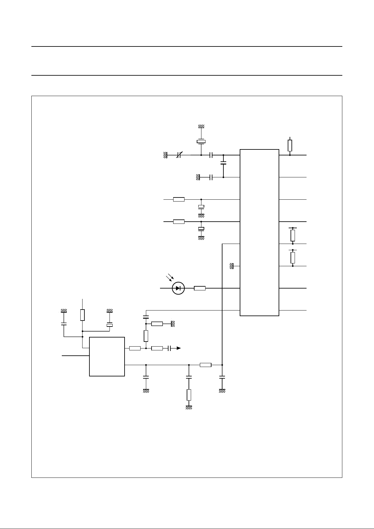
Fig.9 Typical cellular mobile radio application.
ETACS application for:
VCO sensitivity = 11 MHz/V.
Channel spacing = 12.5 kHz.
+
+
+
C12
68 pF
C13
120 pF
G1
9.6 MHz
C8
2-20 pF
C11
39 pF
C9
47 Fµ
R7
68Ω
R8
12Ω
C10
47 Fµ
V
CP
V
CC
1
2
3
4
5
6
8
7
16
15
14
13
12
11
9
10
V
CC
R10
10 k
Ω
V
CC
V
CC
10 kΩ
10 kΩ
SDA
SCL
V
CC
low
current
LED
R9
3.9 kΩ
V3
V
CC
100 nF
R3
12Ω
C5
47 Fµ
modulation
input
VOLTAGE
CONTROLLED
OSCILLATOR
870 to 910
MHz
C6
1 nF
R11
56Ω
R5
18Ω
C17
1 nF
R6
18 Ω
R4
18
Ω
C1
33 nF
C3
180 nF
C2
2.2 nF
R1
18 kΩ
R2
10 kΩ
control voltage
RF output
UMA 1014
MRA404 - 1
Page 15
October 1992 15
Philips Semiconductors Product specification
Low-power frequency synthesizer for
mobile radio communications
UMA1014
PACKAGE OUTLINE
X
w M
θ
A
A
1
A
2
b
p
D
H
E
L
p
Q
detail X
E
Z
e
c
L
v M
A
(A )
3
A
8
9
1
16
y
pin 1 index
UNIT
A
max.
A1A2A
3
b
p
cD
(1)E(1) (1)
eHELLpQZywv θ
REFERENCES
OUTLINE
VERSION
EUROPEAN
PROJECTION
ISSUE DATE
IEC JEDEC EIAJ
mm
inches
1.75
0.25
0.10
1.45
1.25
0.25
0.49
0.36
0.25
0.19
10.0
9.8
4.0
3.8
1.27
6.2
5.8
0.7
0.6
0.7
0.3
8
0
o
o
0.25 0.1
DIMENSIONS (inch dimensions are derived from the original mm dimensions)
Note
1. Plastic or metal protrusions of 0.15 mm maximum per side are not included.
1.0
0.4
SOT109-1
95-01-23
97-05-22
076E07S MS-012AC
0.069
0.010
0.004
0.057
0.049
0.01
0.019
0.014
0.0100
0.0075
0.39
0.38
0.16
0.15
0.050
1.05
0.041
0.244
0.228
0.028
0.020
0.028
0.012
0.01
0.25
0.01 0.004
0.039
0.016
0 2.5 5 mm
scale
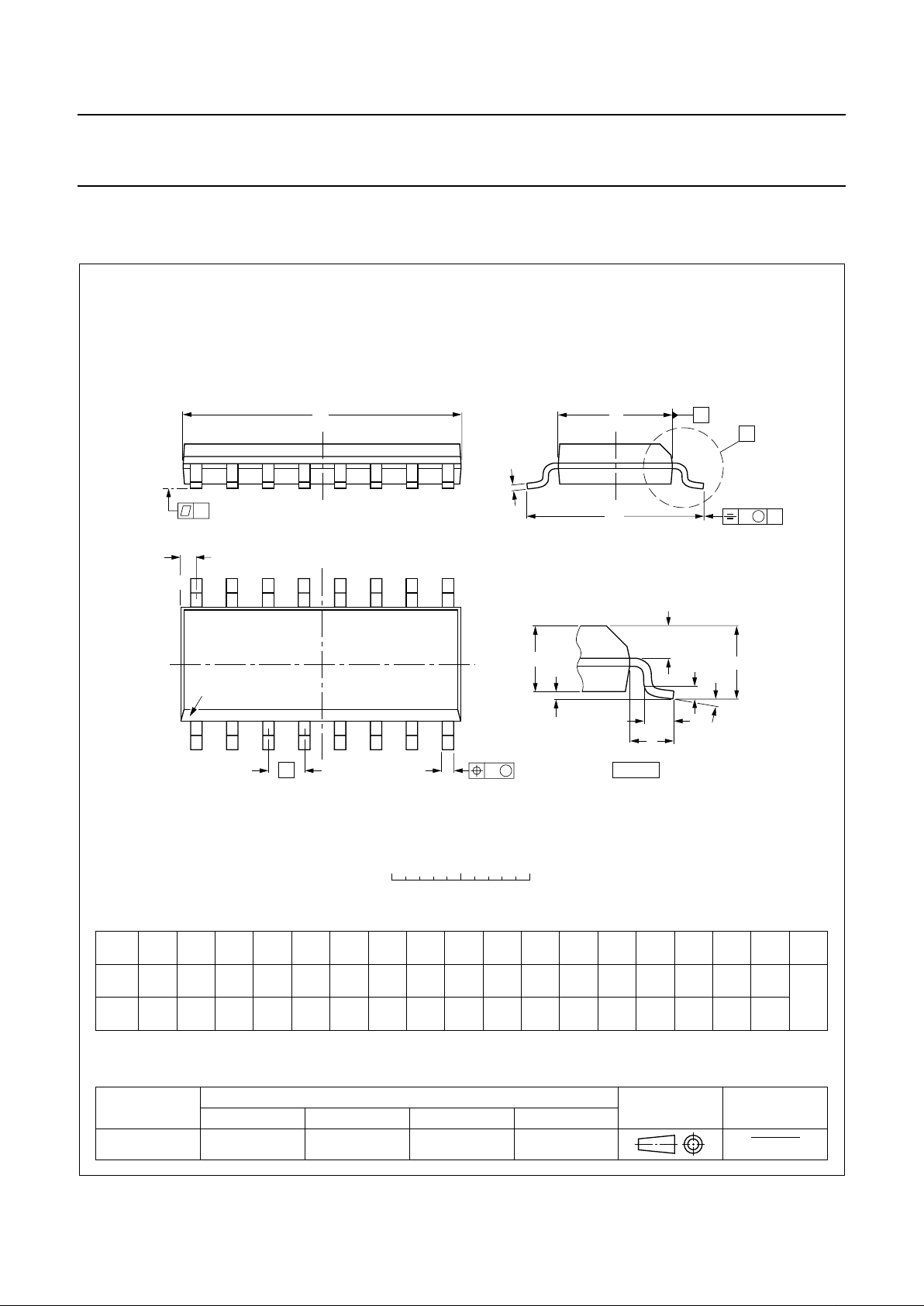
SO16: plastic small outline package; 16 leads; body width 3.9 mm
SOT109-1
Page 16

October 1992 16
Philips Semiconductors Product specification
Low-power frequency synthesizer for
mobile radio communications
UMA1014
SOLDERING
Introduction
There is no soldering method that is ideal for all IC
packages. Wave soldering is often preferred when
through-hole and surface mounted components are mixed
on one printed-circuit board. However, wave soldering is
not always suitable for surface mounted ICs, or for
printed-circuits with high population densities. In these
situations reflow soldering is often used.
This text gives a very brief insight to a complex technology.
A more in-depth account of soldering ICs can be found in
our
“IC Package Databook”
(order code 9398 652 90011).
Reflow soldering
Reflow soldering techniques are suitable for all SO
packages.
Reflow soldering requires solder paste (a suspension of
fine solder particles, flux and binding agent) to be applied
to the printed-circuit board by screen printing, stencilling or
pressure-syringe dispensing before package placement.
Several techniques exist for reflowing; for example,
thermal conduction by heated belt. Dwell times vary
between 50 and 300 seconds depending on heating
method. Typical reflow temperatures range from
215 to 250 °C.
Preheating is necessary to dry the paste and evaporate
the binding agent. Preheating duration: 45 minutes at
45 °C.
Wave soldering
Wave soldering techniques can be used for all SO
packages if the following conditions are observed:
• A double-wave (a turbulent wave with high upward
pressure followed by a smooth laminar wave) soldering
technique should be used.
• The longitudinal axis of the package footprint must be
parallel to the solder flow.
• The package footprint must incorporate solder thieves at
the downstream end.
During placement and before soldering, the package must
be fixed with a droplet of adhesive. The adhesive can be
applied by screen printing, pin transfer or syringe
dispensing. The package can be soldered after the
adhesive is cured.
Maximum permissible solder temperature is 260 °C, and
maximum duration of package immersion in solder is
10 seconds, if cooled to less than 150 °C within
6 seconds. Typical dwell time is 4 seconds at 250 °C.
A mildly-activated flux will eliminate the need for removal
of corrosive residues in most applications.
Repairing soldered joints
Fix the component by first soldering two diagonallyopposite end leads. Use only a low voltage soldering iron
(less than 24 V) applied to the flat part of the lead. Contact
time must be limited to 10 seconds at up to 300 °C. When
using a dedicated tool, all other leads can be soldered in
one operation within 2 to 5 seconds between
270 and 320 °C.
DEFINITIONS
Data sheet status
Objective specification This data sheet contains target or goal specifications for product development
Preliminary specification This data sheet contains preliminary data; supplementary data may be published later.
Product specification This data sheet contains final product specifications.
Limiting values
Limiting values given are in accordance with the Absolute Maximum Rating System (IEC 134). Stress above one or
more of the limiting values may cause permanent damage to the device. These are stress ratings only and operation
of the device at these or at any other conditions above those given in the Characteristics sections of this specification
is not implied. Exposure to limiting values for extended periods may affect device reliability.
Application information
Where application information is given, it is advisory and does not from part of the specification.
Page 17

October 1992 17
Philips Semiconductors Product specification
Low-power frequency synthesizer for
mobile radio communications
UMA1014
LIFE SUPPORT APPLICATIONS
These products are not designed for use in life support appliances, devices, or systems where malfunction of these
products can reasonably be expected to result in personal injury. Philips customers using or selling these products for
use in such applications do so at their own risk and agree to fully indemnify Philips for any damages resulting from such
improper use or sale.
PURCHASE OF PHILIPS I
2
C COMPONENTS
Purchase of Philips I
2
C components conveys a license under the Philips’ I2C patent to use the
components in the I2C system provided the system conforms to the I2C specification defined by
Philips. This specification can be ordered using the code 9398 393 40011.
 Loading...