

Datasheet UM3758-180AM, UM3758-180A, UM3758-120AM, UM3758-120A, UM3758-108BM Datasheet (UMC)
...Page 1
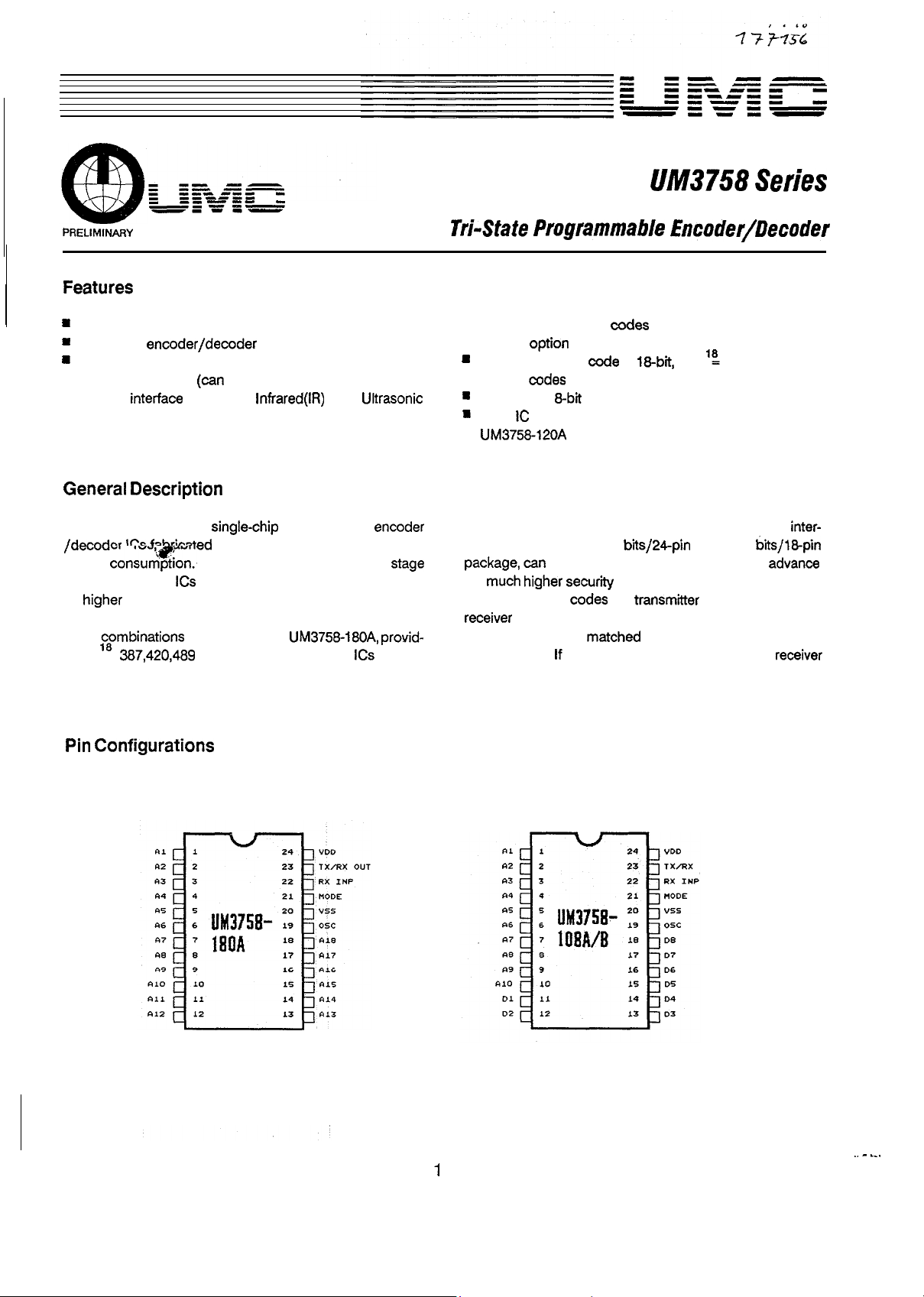
Single-Chip CMOS construction
Single-Chip
Wide operating voltage range : VDO = 3 to 12 Volts
. Built-in RC oscillator
n Easy interface with RF, Infrared(lR) and Ultrasonic
transmission media
n Tri-state(0, 1, open) address codes, some of address
selected by jump wire
use 5 % resistor)
The UM3758 series are
fabricated in CMOS structure for low
power
encoder/decoder
for higher security.
Most
ing 3 =
series provide 4 to 8 data bits for controlling.
They are enhanced for new
to provide many more combinations
are achieved by
combinations. Some
programmable encoder
provid-
of this
codes used as data
by mask
Internal address code is
different ccdes at most
Decoder has 8-bit latch data
Series
n
According to the following information, The
nal address biis, 18
for
the address
the successive two matched address codes will generate
a low pulse. If there were any data bits, the
will latch these data bis at the corresponding pins
for controlling.
for various applications
pin outcompatibleto UM3750
be assigned by customer in
higher
and confidentialii. Whenever
of transmitter transmits, the
or as internal addresses
ie 3
387,428, 489
and 12
Page 2
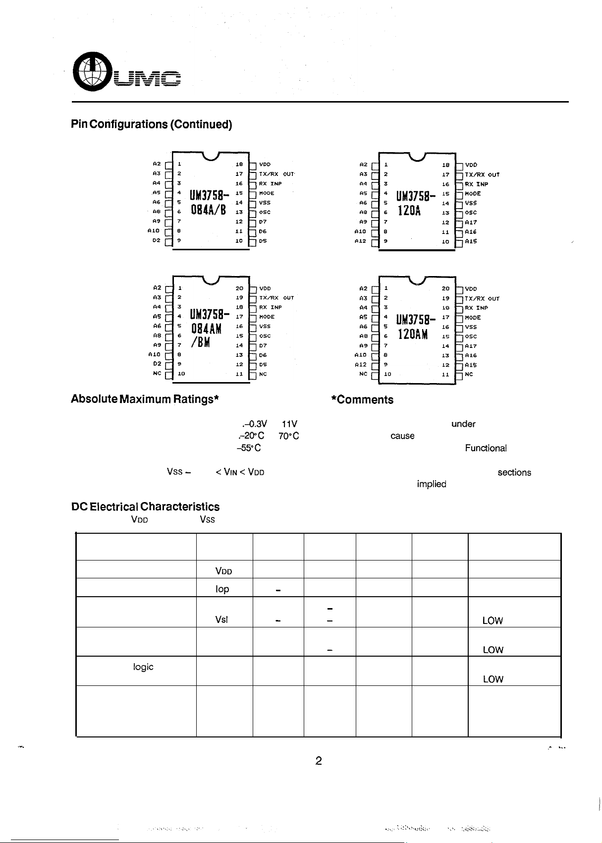
UM3758 Series
Power Supply Voltage . . . . . . . . . .-0.3V to
Operating Temperature . . . . . . . .
Storage Temperature (Tstg) . . . . .
to
to 150°C
Apply Voltage on any Pin . . . . . . . . . . . . . .
(TA = 25°C ,
Parameter
Operating voltage
0.3
= 9 Volts ,
+ 0.3
= OV unless otherwise specified)
Symbol
Min.
3.0
Operating current
Schmitt Trigger input
Vsh
6
level
Other pins input
level
Output pin logic
level
Vih
Vil
Voh
Vol
8.5
0
8.5
0
DATA output current
HIGH level
LOW level
lohd
lold
9
9
Stresses above those listed under “Absolute Maximum
Ratings’ may
permanent darnage to the device.
These are stress ratings only. Functional Operation of
this device at these or any other conditions above
those indicated in the operational sections of this
specification is not implied and exposure to absolute
TYP.
Max.
12
1.2
2
9
0.5
9
1
Unit
V
mA
V
V
V
v
V
v
Conditions
HIGH
HIGH
HIGH
VDD = 12V
mA
mA
Voh = 6V
Vol = 6V
Page 3
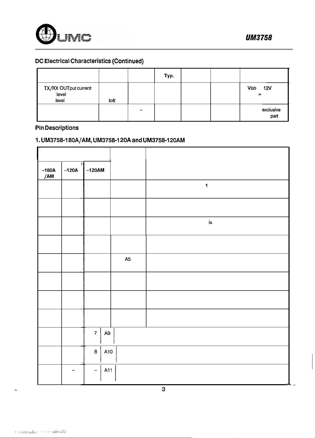
Series
Parameter Symbol Min.
HIGH level
LOW level
Operating frequency
loht
F
UM3758 UM3758
1
2
Pin Number
1
UM37584
UM3758
1
35
Designation
Al
A2
15
Max.
160
Unit ,
mA
mA
KHz
Descripti.on
Address select line
and open
Address select line 2 is tri-state indicated as 0, 1
and open
is tri-state indicated as 0, 1
Conditions
=
Voh
6V
Vol
= 6V
+ 15%
of external
3
4
5
6
10
11
2
3
4
5
7
8
9
6
7
8
2
3 A4
4 A5
5
6
A3
A6
A7
A8
and open
and open
and open
Address select line 3 is tri-state indicated as 0, 1
and open
Address
and open
Address
and open
Address select line
and open
Address
and open
Address
and open
Address select line 9 is tri-state indicated as 0, 1
Address select line 10 is tri-state indicated as 0, 1
Address select line 11 is tri-state indicated as 0, 1
select
select
select
select
line
line
line
line 8
4 is
5 is
6 is
7
is
is
tri-state
tri-state
tri-state
tri-state
tri-state
indicated as
indicated as
indicated as
indicated as
indicated
as
0,
0,
0,
0,
0,
1
1
1
1
1
Page 4
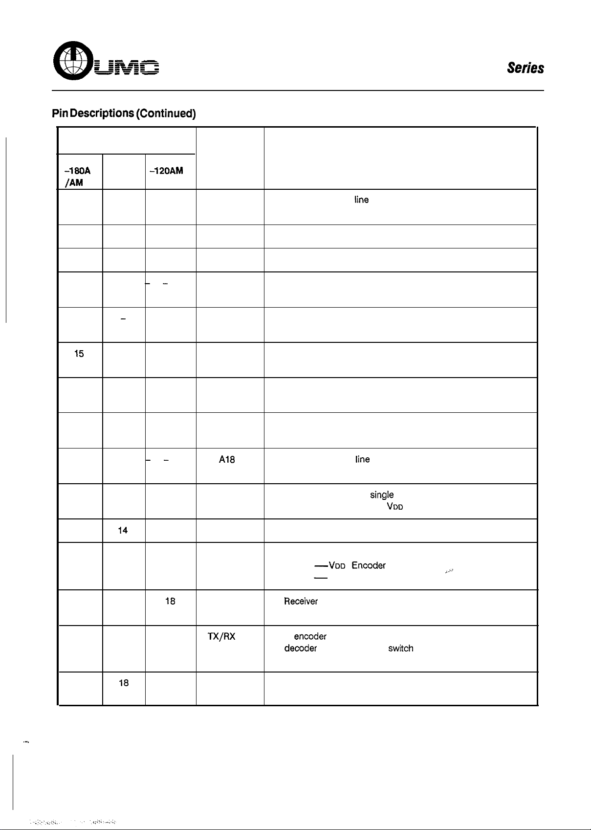
UM3758
Pin Number
UM3758 UM3758 UM3758
-12OA
12
9
9
10
11
13
14
12
13
16
10
11
Designation
Al2
NC
NC
Al3
Al4
Al5
Al6
Description
Address select line 12 is tri-state indicated as 0, 1
and open
No connection
Noconnection
Address select line 13 is tri-state indicated as 0, 1
and open
Address select line 14 is tri-state indicated as 0, 1
and open
Address select line 15 is tri-state indicated as 0, 1
and open
Address select line 16 is tri-state indicated as 0, 1
and open
17 12
16
19
13
20
21
22
23
15
16
17
24
14
15
17
19
20
Al7
osc
vss
MODE
RXINP
VDD
Address select line 17 is tri-state indicated as 0, 1
and open
Address select line 16 is tri-state indicated as 0, 1
and open
R.C. input pin for
connected from this pin to
pin oscillator. A resistor is
and a capacitor to Vss
The ground pin for UM3756
This pin is used to select transmit or receive mode
MODE
MODE
: Encoder mode
Vss : Decoder mode
input pin. Receives waveform from the detect
circuit
In encoder mode, this pin will transmit waveform; in
is OK
The positive power supply of UM3756
4
Page 5
UM3758 Series
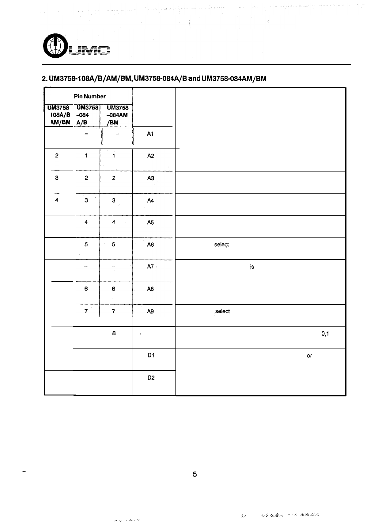
UM3758=108A/B/AM/BM, UM3758-084A/B
Designation
1
5
6
UM3758-084AM/BM
Description
Address select line 1 is tri-state indicated as 0, 1
and open
Address select line 2 is tri-state indicated as 0, 1
and open
Address select line 3 is tri-state indicated as 0, 1
and open
Address select line 4 is tri-state indicated as 0, 1
and open
Address select line 5 is tri-state indicated as 0, 1
and open
Address select line 6 is triistate indicated as 0, 1
and open
10
11
12
7
a
9
a
9
9
Al0
Address select line 7 is tri-state indicated as 0, 1
and open
Address select line 8 is tri-state indicated as 0, 1
and open
Address
and open
Address select line 10 is tri-state indicated as
and open
Data output pin 1, states are either HIGH (1 or open)
or LOW (0)
Data output pin 2, states are either HIGH (1 or open)
or LOW (0)
line 9 is tri-state indicated as 0, 1
.
Page 6
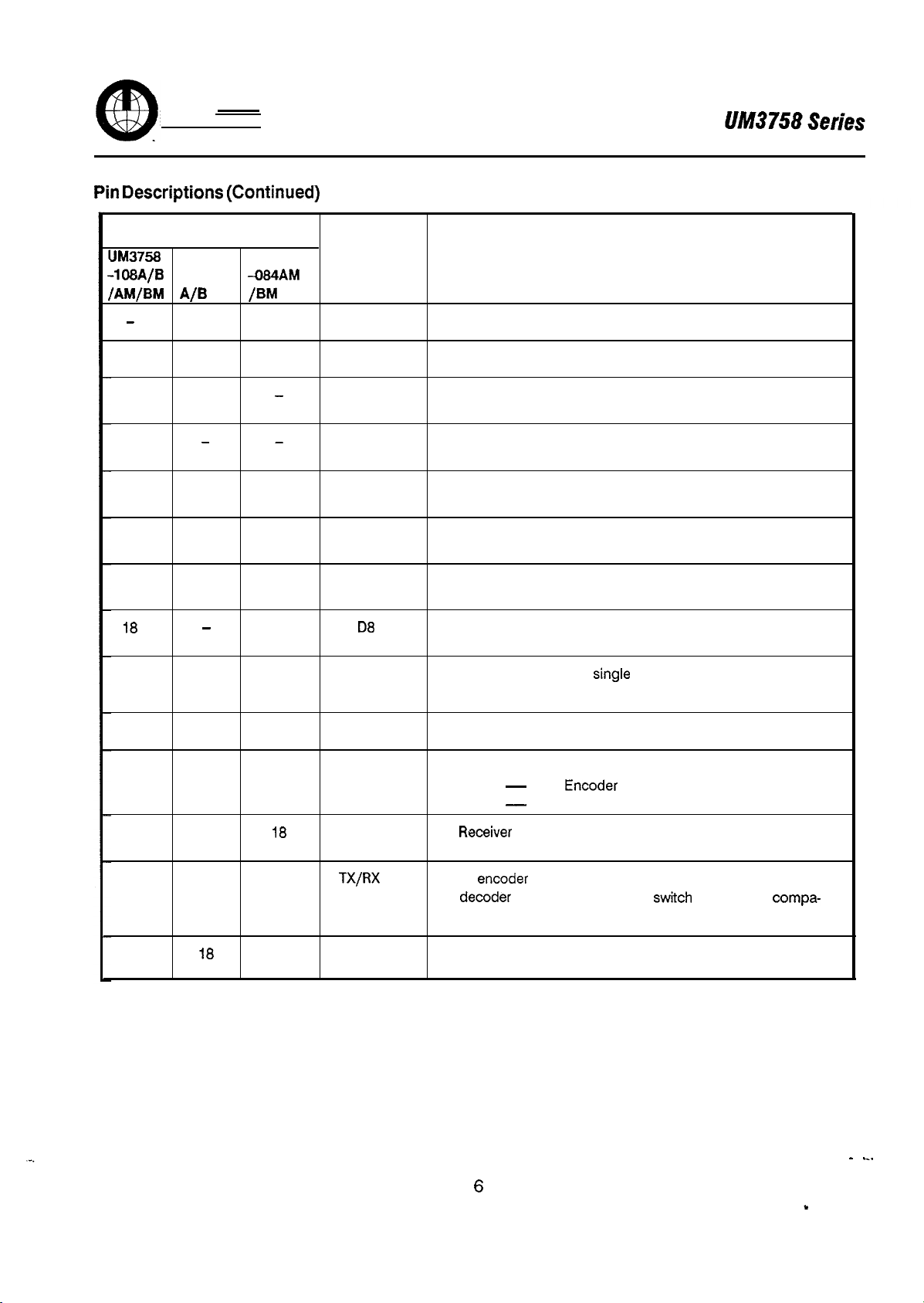
Pin Number
UM3758 UM3758
13
14
15
16
17
19
10
11
12
13
10
11
12
13
14
15
Designation
NC
NC
D3
D4
D5
D6
D7
osc
Description
Noconnection
No connection
Data output pin 3, states are either HIGH (1 or open)
or LOW (0)
Data output pin 4, states are either HIGH (1 or open)
or LOW (0)
Data output pin 5, states are either HIGH (1 or open)
or LOW (0)
Data output pin 6, states are either HIGH (1 or open)
or LOW (0)
Data output pin 7, states are either HIGH (1 or open)
or LOW (0)
Data output pin 6, states are either HIGH (1 or open)
or LOW (0)
R.C. input pin for
connected from this pin to VDO and a capacitor to Vss
pin oscillator. A resistor is
20
21
22 16
23
24
15
17
14
16
17
19
20
vss
MODE
RXINP
OUT
VDD
The ground pin for UM3756
This pin is used to select transmit or receive modes
MODE
MODE
circuit
In encoder mode, this pin will transmit waveform; in
rison is OK
The positive power supply of UM3756
VDO : Encoder mode
Vss : Decoder mode
input pin. Receives waveform from the detect
to LOW if compa-
Page 7

-
em----
UM3758
General
The operating mode of the UM3756 series is controlled
by the MODE pin. When the ‘MODE’ pin is connected to
VDO the circuit will automatically switch to encoder
mode, then ‘TX/RX OUT’ pin
‘RX
pin act as an idle pin. When ‘MODE’ pin is
as data out pin and
connected to Vss the circuit will switch to decoder
mode, then ‘TX/RX OUT” pin will switch to LOW if
comparison is
and
otherwise this pin will keep HIGH,
receives waveform from detect circuit.
Mode
The encoder mode is selected by connecting “MODE
pin to
The transmit sequence is initiated by the power
nection and continuously transmits till power down.
Part
Number
Address
Bits
Address
Combinations
(see Fig.
consecutive long
A logic zero is encoded as two
a logic one as two con-
secutive short pulses and an open as a long pulse
followed by a short pulse.
is encoded into logic
is the
as the address pulse (see Fig.
the state of data pin is either one or
is one when connected to
transmitted data bit
or one and the data pulse
ie.,
The data
or open and
when
connected to Vss.
The UM3756160A samples the 18 bit tri-state address
and encodes this parallel address data for trans-
mitting. These 16 address pins may
three states (0, 1, open) allowing 3
possible combinations then
UM3758120A provides
in either of
address and allows 3 = 531,441 possible
binations.
The UM37561
and
provide address
and data bits, as described in Table 1.
Data
Bits
Data
Combinations
10
a 6,561
59,049
4
256
16
Table 1
Decoder Mode
The decoder mode is selected by connecting “MODE” pin
to vss.
The decoder receives the serial data from the detect
circuit and outputs the comparison result or data, if
(ex. UM375&106A/B) are assumed to be address bi.
If the address bits
the address bits from
detect circuit, the next eight data bits are stored
and
to the last valid data stored. When the
it is valid. The received data may inolude two types
without data and with data.
must
again, and if it does, the data bits are
against the previous stored data biis. If
For decoder without data
such as
and
the two words (eight bits data
of data
the data is transferred to the output data pins
received; if two successive address words
address bis of
switch to LOW and
the “TX/RX OUT” pin will
successive unmatched address
the
words will cause ‘TX/RX OUT” pin to return to HIGH
(see Fig. 3-l).
For decoder with data IC, such as UM375&106A/B and
D2 to
pins will
switches to HIGH; for
will
(see Fig. 3-2). Although the address bits
state (0, 1,
either one or
If the decoder is momentary type, the data
the data till the ‘TX/RX OUT’ pin
decoder, the data pins
the data
the next valid data appears
open), the data information must be
An open state will be decoded as
tri-
a logic one. The above table (Table 1) also describes ___
..
examined bit by bi as received. The first 10 bits
these (decoder with data).
Page 8

------
--
Tri-State Encoded Pulses
UM3758
Fig.
10.- t
Decoder Mode (without data) :
10.
Fig. 2
Fig.
3 -1
Page 9

UM3758
Decoder Mode (with data) :
OUT
UM3758 Operation Flowchart (without data bit)
RDDRESS
Fig. 3 -2
WITCH
Page 10

---
-m-m-
----d
UM3758 Series
UM3758 Operation
(with data bit)
* Note :
Type
For MOMENTARY Type
* Address MISMATCH INCLUDES
Keep current data
All Data fall to LOW
NO SIGNAL IN
Page 11

UM3758 Series
U
24
PF
23
U
(A)
Use Three-Contact Pushbutton
Note: ETD
ETD
8-Pin Tri-State DIP switch made by EXCEL CELL ELECTRONIC CO., LTD. IN TAIWAN R.O.C.
lC-Pin Tri-State DIP switch made by EXCEL CELL ELECTRONIC CO., LTD. IN TAIWAN R.O.C.
Q
Page 12

Application Circuits (Continued)
(B) Use Normal Two-Contact Pushbutton
1 Appiication Circuit with Data Bit High to Low
UM3758 Series
c
PF
,
(B)
2 Application Circuit with Data Bit Lowto High
AS
LON
SN1
1
12
:
UHICE
Page 13
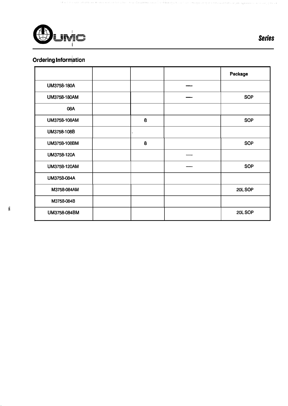
UM3758
Part No. Addresses
18
18
UM37581 08A
10
10
10
10
12
12
U
U
8
8
8
Data
0
0
8
8
0
0
4
4 LATCHED
4
4
Data Output Type
IATCHED
IATCHED
MOMENTARY
MOMENTARY
LATCHED
MOMENTARY
MOMENTARY
24L DIP
24L BOP
24L DIP
24L
24L DIP
24L
18L DIP
20L
18LDIP
18LDIP
SOP
13
Page 14

UM3758 Series
Symbol
A
B
Dimensions in
0.210 Max. 5.33
0.010 Min. 0.25 Min.
0.018
-0.002
Dimensions in mm
3.94
0.46 +O.lO
unit :
-0.05
0.010 +
-0.002
E
Note:
1. The max value of dlmenson D includes end flash
2. The dimenslon
3. The dimension S
4. All dimensions are based
1 250TYP
0.655~0035
0.090 Max
doesn’t include
end flash.
14
British
1.52
0.25
fins.
-0.05
-0.05
2.54r0.25
16 64+0.69
2.29 Max.
Page 15

UM3758 Series
Symbol
A
Dimensions in
0.110 Max.
Dimensions in mm
2.79 Max.
unit :
D
F
HE
S
Y
Note:
The max value of dimension
2. The dimension E doesn’t include
3. The dimension el
reference only.
4. The dimension S includes end flash.
5. All dimensions are based on British
0 295+0.010
0.050
0.006
0.370 NOM
036+0.008
0.055
0.006
0.040 Max.
0.006 Max.
for PC Board surface mount pad
7.49
0.25
9.40 NOM
10.31
0.91
1.02 Max.
0.15 Max.
includes end flash.
Page 16

UM3758 Series
Plane
Plane
Dimensions in
0.175 Max.
0.010 Min. 0.25 Min.
0
Dimensions in mm
4.45 Max.
E
0.018 +
0.002
-0.002
0.002
0.9OOTYP
010 2.54
L
0.345 + 0.035
S
Note:
1. The max vaiue of dimensloq
2. The dimenslon Et doesn’t Include
3. The dimension
4. All dimensions are based on British
0.055 Max.
includes end flash.
16
0.46
-0.05
1.52
-0.05
0.25
includes end flash.
7.62
3.30i0.25
1.40 Max.
0.25
0.25
0.05
Page 17

UM3758
DETAIL F
unit :
SEE DETAIL F
Symbol
A
Al
A2
b
D
Dimensions in
0.106 Max
0.004 Min
0.092
+
0.004
0.016
0.002
0.010
0.002
0.504 TYP (0.524 Max)
0.055
0.008
0.042 Max
0.006 Max.
Dimensions in mm
2.69 Max
0.10 Min
0.41
-0.05
0.25
-0.05
12.80 TYP (13.31
1.40 *0.20
1.07 Max
0.15 Max
1
Note:
1. The max value of dimension D includes end flash.
2. The dimensions E doesn’t include
3. The
reference oniy.
4. The
5. All dimensions are based on British
el is for PC Board surface mount pad
S includes end flash
fins.
Page 18

UM3758 Series
The information appearing in this publication is believed to be accurate. Integrated circuits sold by UMC
are covered by the warranty and patent indemnification provisions stipulated in the terms of sale only.
UMC makes no warranty, expressed, statutory, implied or by description regarding the information in this
publication or regarding the freedom of the described chip from patent infringement. Furthermore, UMC
makes no warranty of merchantability or fitness for any purpose. UMC reserves the right to halt
tion or alter specifications and
verify that the data sheets and other information in this publication are current before placing
orders.
require extended temperature range, unusual environmental requirements, or high reliability applications,
e.g.
without additional processing by UMC for such applications.
in this document are for reference purposes only.
UMC has no sales or Service functions in the U.S.A. and therefore does not intend to sell its products
in this market.
at any time without
Accordingly, the reader is cautioned
are specifically not recommended
Also, please note that Application Circuits
 Loading...