

Page 1
ULN2003,04APG/AFWG
TOSHIBA Bipolar Digital Integrated Circuit Silicon Monolithic
ULN2003APG,ULN2003AFWG,ULN2004APG,ULN2004AFWG
(Manufactured by Toshiba Malaysia)
7ch Darlington Sink Driver
The ULN2003APG/AFWG Series are high−voltage, high−current
darlington drivers comprised of seven NPN darlington pairs.
All units feature integral clamp diodes for switching inductive
loads.
Applications include relay, hammer, lamp and display (LED)
drivers.
The suffix (G) appended to the part number represents a Lead
(Pb)-Free product.
Features
Output current (single output): 500 mA max
High sustaining voltage output: 50 V min
Output clamp diodes
Inputs compatible with various types of logic
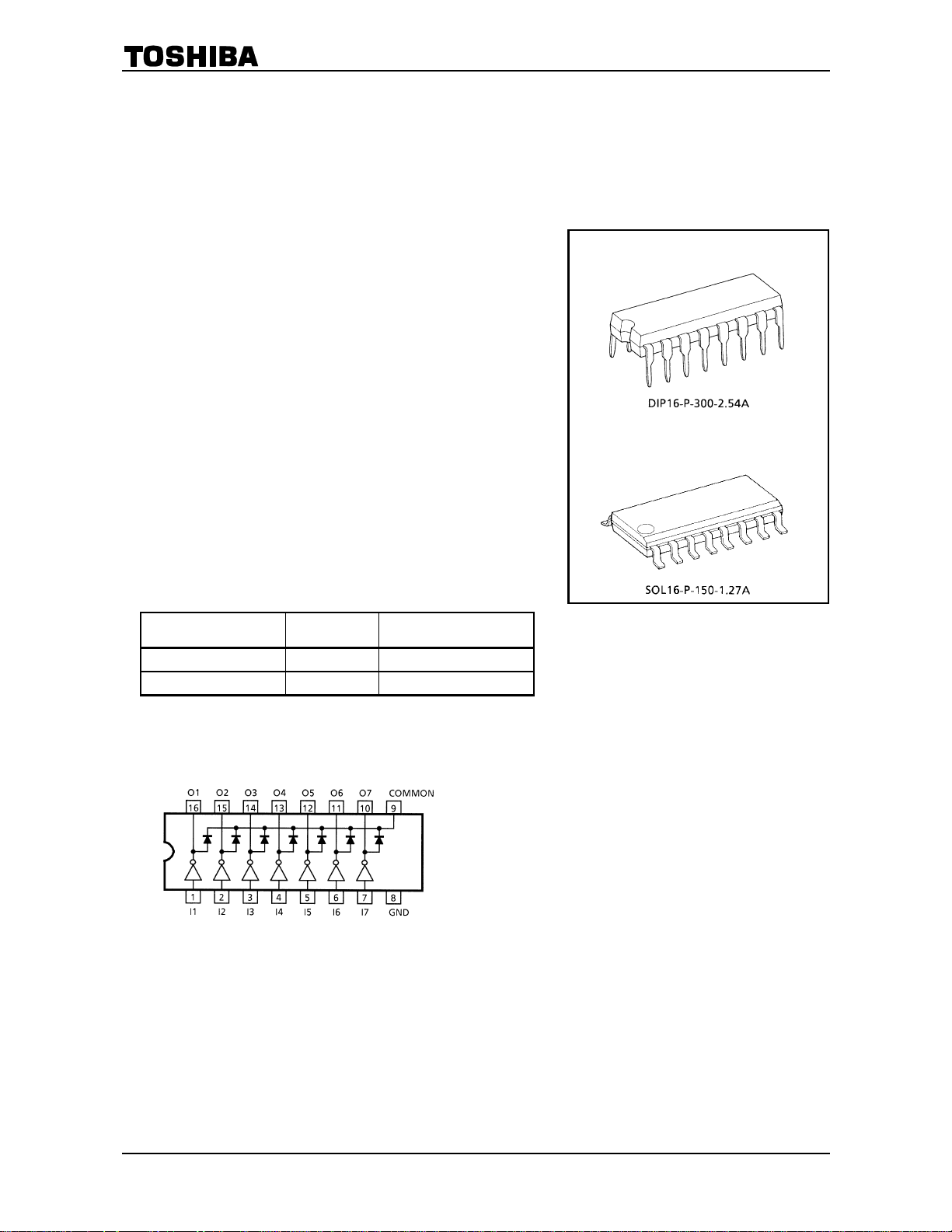
Package Type-APG: DIP-16pin
Package Type-AFWG: SOL-16pin
Type
ULN2003APG/AFWG 2.7 kΩ TTL, 5 V CMOS
ULN2004APG/AFWG 10.5 kΩ 6~15 V PMOS, CMOS
Pin Connection
(top view)
Input Base
Resistor
Designation
ULN2003APG
ULN2004APG
ULN2003AFWG
ULN2004AFWG
Weight
DIP16−P-300-2.54A : 1.11 g (typ.)
SOL16−P-150-1.27A : 0.15 g (typ.)
1
2006-06-14
Page 2
ULN2003,04APG/AFWG
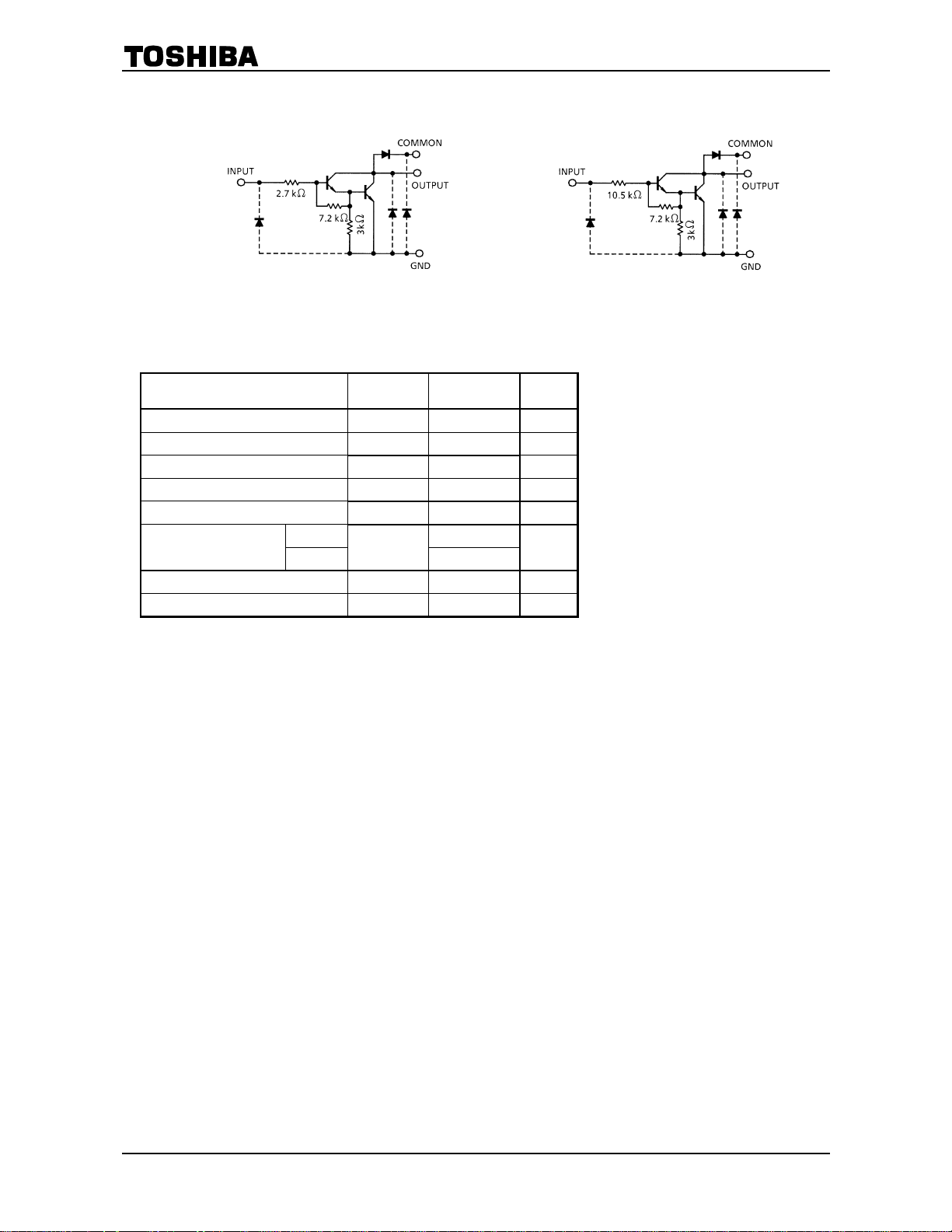
Schematics
(each driver)
ULN2003APG/AFWG ULN2004APG/AFWG
Note: The input and output parasitic diodes cannot be used as clamp diodes.
Absolute Maximum Ratings
Characteristic Symbol Rating Unit
Output sustaining voltage V
Output current I
Input voltage V
Clamp diode reverse voltage V
Clamp diode forward current I
Power dissipation
Operating temperature T
Storage temperature T
APG 1.47
AFWG
(Ta = 25°C)
CE (SUS)
OUT
IN
R
F
P
D
opr
stg
0.5~50 V
−
500 mA/ch
0.5~30 V
−
50 V
500 mA
1.25 (Note)
−40~85 °C
55~150 °C
−
W
Note: On PCB (Test Board: JEDEC 2s2p)
2
2006-06-14
Page 3
ULN2003,04APG/AFWG
Recommended Operati ng Co ndi tions
Characteristic Symbol Test Condition Min Typ. Max Unit
Output sustaining voltage V
APG
Output current
AFWG
Input voltage V
Input voltage
(output on)
Input voltage
(output off)
Clamp diode reverse voltage V
Clamp diode forward current IF
Power dissipation
ULN2003A 2.8 ⎯ 24
ULN2004A
ULN2003A 0 ⎯ 0.7
ULN2004A
APG Ta
AFWG
V
V
Note: On PCB (Test Board: JEDEC 2s2p)
CE (SUS)
I
OUT
IN
IN (ON)
IN (OFF)
R
PD
(Ta = −40 to 85°C)
0 ⎯ 50 V
T
= 25 ms
pw
7 Circuits
Ta = 85°C
T
= 120°C
j
0
I
= 400 mA
OUT
h
= 800
FE
0 ⎯ 1.0
⎯ ⎯ 50 V
85°C
=
Ta = 85°C (Note)
Duty = 10% 0 ⎯ 350
Duty = 50% 0 ⎯ 100
Duty = 10% 0
Duty = 50% 0
300
⎯
90
⎯
24 V
⎯
6.2 ⎯ 24
⎯
⎯
⎯
350 mA
⎯
0.76
⎯
0.65
⎯
mA/ch
V
V
W
3
2006-06-14
Page 4
ULN2003,04APG/AFWG
Electrical Characteristics
Characteristic Symbol
Output leakage current I
Collector−emitter saturation voltage V
DC Current transfer ratio h
Input current
(output on)
Input current (output off) I
ULN2003A VIN = 2.4 V, I
ULN2004A
(Ta = 25°C unless otherwise noted)
Test
Circuit
1
CEX
2
CE (sat)
FE
I
IN (ON)
IN (OFF)
2 VCE = 2 V, I
3
4 I
ULN2003A
Input voltage
(output on)
V
IN (ON)
5
ULN2004A
Clamp diode reverse current IR 6
Clamp diode forward voltage V
Input capacitance C
Turn−on delay t
Turn−off delay t
IN
ON
OFF
F
7 IF = 350 mA ⎯ ⎯ 2.0 V
⎯ ⎯ 15 ⎯ pF
8
8
Test Condition Min Typ. Max Unit
VCE = 50 V, Ta = 25°C ⎯ ⎯ 50
= 50 V, Ta = 85°C ⎯ ⎯ 100
V
CE
I
= 350 mA, IIN = 500 µA ⎯ 1.3 1.6
OUT
I
= 200 mA, IIN = 350 µA
OUT
I
= 100 mA, IIN = 250 µA
OUT
= 350 mA 1000
OUT
= 350 mA ⎯ 0.4 0.7
OUT
V
= 9.5 V, I
IN
= 500 µA, Ta = 85°C 50 65 ⎯ µA
OUT
V
= 2 V
CE
h
= 800
FE
= 350 mA ⎯ 0.8 1.2
OUT
I
= 350 mA ⎯ ⎯ 2.6
OUT
I
= 200 mA ⎯ ⎯ 2.0
OUT
I
= 350 mA
OUT
= 200 mA
I
OUT
VR = 50 V, Ta = 25°C
V
= 50 V, Ta = 85°C ⎯ ⎯ 100
R
V
= 50 V, RL = 125 Ω
OUT
C
= 15 pF
L
V
= 50 V, RL = 125 Ω
OUT
C
= 15 pF
L
1.1 1.3
⎯
0.9 1.1
⎯
⎯
⎯
4.7
⎯
4.4
⎯
50
⎯
⎯
⎯
⎯
⎯ 0.1 ⎯
0.2 ⎯
⎯
A
µ
V
mA
V
µA
µs
4
2006-06-14
Page 5

Te st Cir cuit
ULN2003,04APG/AFWG
1. I
CEX
4. I
IN (OFF)
7. VF
2. V
CE (sat), hFE
5. V
IN (ON)
3. I
IN (ON)
6. IR
5
2006-06-14
Page 6
ULN2003,04APG/AFWG
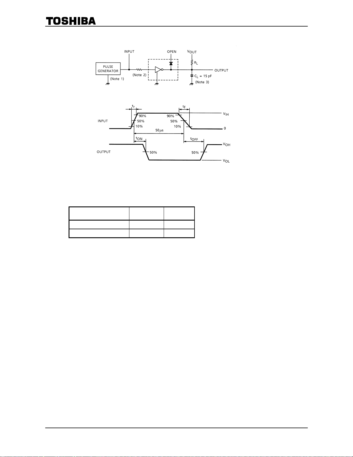
8. tON, t
Note 1: Pulse width 50 µs, duty cycle 10%
Note 2: See below
Input Condition
OFF
Output impedance 50 Ω, t
≤ 5 ns, tf ≤ 10 ns
r
Type Number R1 VIH
ULN2003A 0 3 V
ULN2004A 0 8 V
Note 3: CL includes probe and jig capacitance.
Precautions for Using
This IC does not include built-in protection circuits for excess current or overvoltage.
If this IC is subjected to excess current or overvoltage, it may be destroyed.
Hence, the utmost care must be taken when systems which incorporate this IC are designed.
Utmost care is necessary in the design of the output line, COMMON and GND line since IC may be destroyed
due to short−circuit between outputs, air contamination fault, or fault by improper grounding.
6
2006-06-14
Page 7
ULN2003,04APG/AFWG
7
2006-06-14
Page 8
ULN2003,04APG/AFWG
2.00
1.75
(W)
(1)
1.50
D
(2)
1.25
1.00
0.75
P
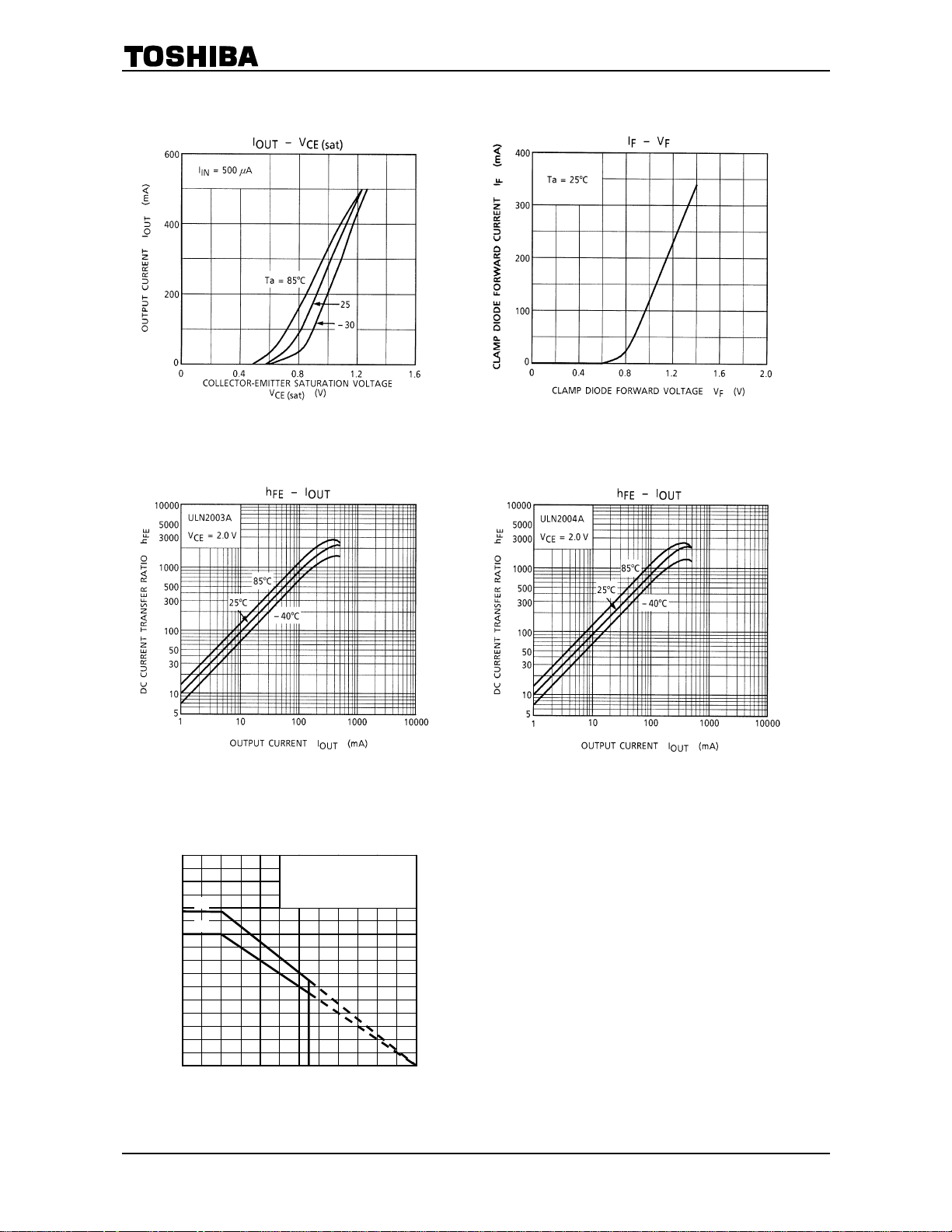
– Ta
D
(1) Type-APG free air
(2) Type-AFWG on PCB
(Test Board: JEDEC 2s2p)
0.50
Power dissipation P
0.25
0
0
25 100 125 75
Ambient temperature Ta (°C)
15050
8
2006-06-14
Page 9
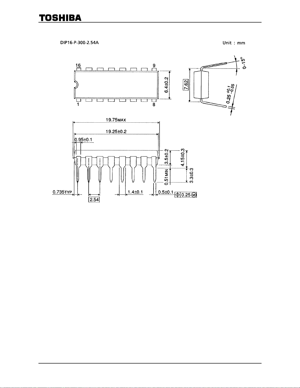
Package Dimensions
ULN2003,04APG/AFWG
Weight: 1.11 g (typ.)
9
2006-06-14
Page 10
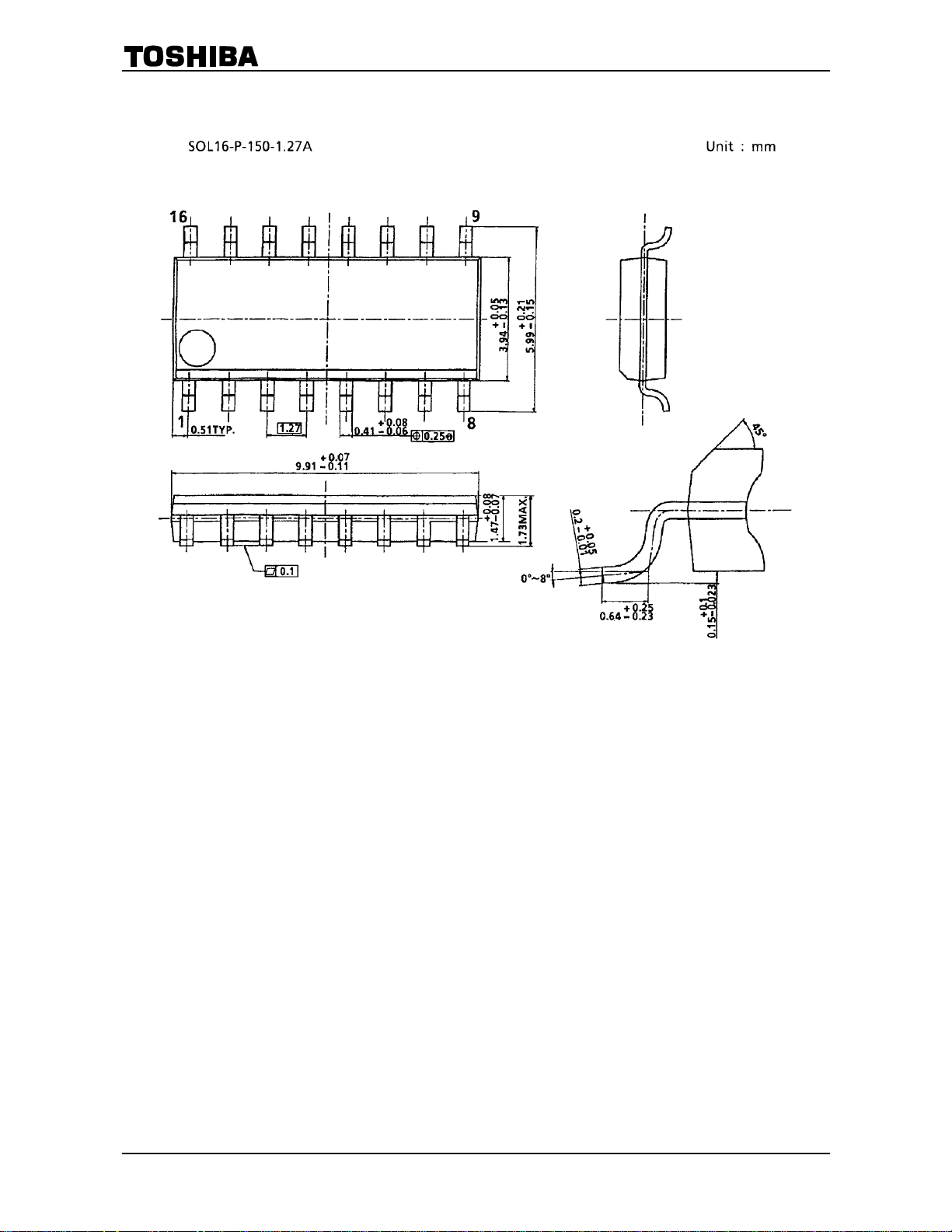
Package Dimensions
ULN2003,04APG/AFWG
Weight: 0.15 g (typ.)
10
2006-06-14
Page 11

Notes on Contents
1. Equivalent Circuits
The equivalent circuit diagrams may be simplified or some parts of them may be omitted for explanatory
purposes.
2. Test Circuits
Components in the test circuits are used only to obtain and confirm the device characteristics. These
components and circuits are not guaranteed to prevent malfunction or failure from occurring in the
application equipment.
IC Usage Considerations
Notes on Handling of ICs
(1) The absolute maximum ratings of a semiconductor device are a set of ratings that must not be
exceeded, even for a moment. Do not exceed any of these ratings.
Exceeding the rating(s) may cause the device breakdown, damage or deterioration, and may result
injury by explosion or combustion.
(2) Use an appropriate power supply fuse to ensure that a large current does not continuously flow in
case of over current and/or IC failure. The IC will fully break down when used under conditions that
exceed its absolute maximum ratings, when the wiring is routed improperly or when an abnormal
pulse noise occurs from the wiring or load, causing a large current to continuously flow and the
breakdown can lead smoke or ignition. To minimize the effects of the flow of a large current in case of
breakdown, appropriate settings, such as fuse capacity, fusing time and insertion circuit location, are
required.
(3) If your design includes an inductive load such as a motor coil, incorporate a protection circuit into the
design to prevent device malfunction or breakdown caused by the current resulting from the inrush
current at power ON or the negative current resulting from the back electromotive force at power OFF.
IC breakdown may cause injury, smoke or ignition.
Use a stable power supply with ICs with built-in protection functions. If the power supply is unstable,
the protection function may not operate, causing IC breakdown. IC breakdown may cause injury,
smoke or ignition.
(4) Do not insert devices in the wrong orientation or incorrectly.
Make sure that the positive and negative terminals of power supplies are connected properly.
Otherwise, the current or power consumption may exceed the absolute maximum rating, and
exceeding the rating(s) may cause the device breakdown, damage or deterioration, and may result
injury by explosion or combustion.
In addition, do not use any device that is applied the current with inserting in the wrong orientation
or incorrectly even just one time.
(5) Carefully select external components (such as inputs and negative feedback capacitors) and load
components (such as speakers), for example, power amp and regulator.
If there is a large amount of leakage current such as input or negative feedback condenser, the IC
output DC voltage will increase. If this output voltage is connected to a speaker with low input
withstand voltage, overcurrent or IC failure can cause smoke or ignition. (The over current can cause
smoke or ignition from the IC itself.) In particular, please pay attention when using a Bridge Tied
Load (BTL) connection type IC that inputs output DC voltage to a speaker directly.
ULN2003,04APG/AFWG
11
2006-06-14
Page 12

Points to Remember on Handling of ICs
(1) Heat Radiation Design
In using an IC with large current flow such as power amp, regulator or driver, please design the
device so that heat is appropriately radiated, not to exceed the specified junction temperature (Tj) at
any time and condition. These ICs generate heat even during normal use. An inadequate IC heat
radiation design can lead to decrease in IC life, deterioration of IC characteristics or IC breakdown. In
addition, please design the device taking into considerate the effect of IC heat radiation with
peripheral components.
(2) Back-EMF
When a motor rotates in the reverse direction, stops or slows down abruptly, a current flow back to
the motor’s power supply due to the effect of back-EMF. If the current sink capability of the power
supply is small, the device’s motor power supply and output pins might be exposed to conditions
beyond absolute maximum ratings. To avoid this problem, take the effect of back-EMF into
consideration in system design.
ULN2003,04APG/AFWG
12
2006-06-14
Page 13
About solderability, following conditions were confirmed
•
Solderability
(1) Use of Sn-37Pb solder Bath
· solder bath temperature = 230°C
· dipping time = 5 seconds
· the number of times = once
· use of R-type flux
(2) Use of Sn-3.0Ag-0.5Cu solder Bath
· solder bath temperature = 245°C
· dipping time = 5 seconds
· the number of times = once
· use of R-type flux
ULN2003,04APG/AFWG
RESTRICTIONS ON PRODUCT USE
• The information contained herein is subject to change without notice. 021023_D
• TOSHIBA is continually working to improve the quality and reliability of its products. Nevertheless, semiconductor
devices in general can malfunction or fail due to their inherent electrical sensitivity and vulnerability to physical
stress. It is the responsibility of the buyer, when utilizing TOSHIBA products, to comply with the standards of
safety in making a safe design for the entire system, and to avoid situations in which a malfunction or failure of
such TOSHIBA products could cause loss of human life, bodily injury or damage to property.
In developing your designs, please ensure that TOSHIBA products are used within specified operating ranges as
set forth in the most recent TOSHIBA products specifications. Also, please keep in mind the precautions and
conditions set forth in the “Handling Guide for Semiconductor Devices,” or “TOSHIBA Semiconductor Reliability
Handbook” etc.
• The TOSHIBA products listed in this document are intended for usage in general electronics applications
(computer, personal equipment, office equipment, measuring equipment, industrial robotics, domestic appliances,
etc.). These TOSHIBA products are neither intended nor warranted for usage in equipment that requires
extraordinarily high quality and/or reliability or a malfunction or failure of which may cause loss of human life or
bodily injury (“Unintended Usage”). Unintended Usage include atomic energy control instruments, airplane or
spaceship instruments, transportation instruments, traffic signal instruments, combustion c ontrol instruments,
medical instruments, all types of safety devices, etc. Unintended Usage of TOSHIBA products listed in this
document shall be made at the customer’s own risk.
• The products described in this document shall not be used or embedded to any downstream products of which
manufacture, use and/or sale are prohibited under any applicable laws and regulations.
• The information contained herein is presented only as a guide for the applications of our products. No
responsibility is assumed by TOSHIBA for any infringements of patents or other rights of the third parties which
may result from its use. No license is granted by implication or otherwise under any patent or patent rights of
TOSHIBA or others.
021023_A
021023_B
060106_Q
021023_C
060116EBA
• The products described in this document are subject to the foreign exchange and foreign trade laws. 021023_E
13
2006-06-14
 Loading...