

Page 1
5140
PROTECTED POWERHALL
®
SENSOR:
LAMP/SOLENOID DRIVER
5140
Data Sheet
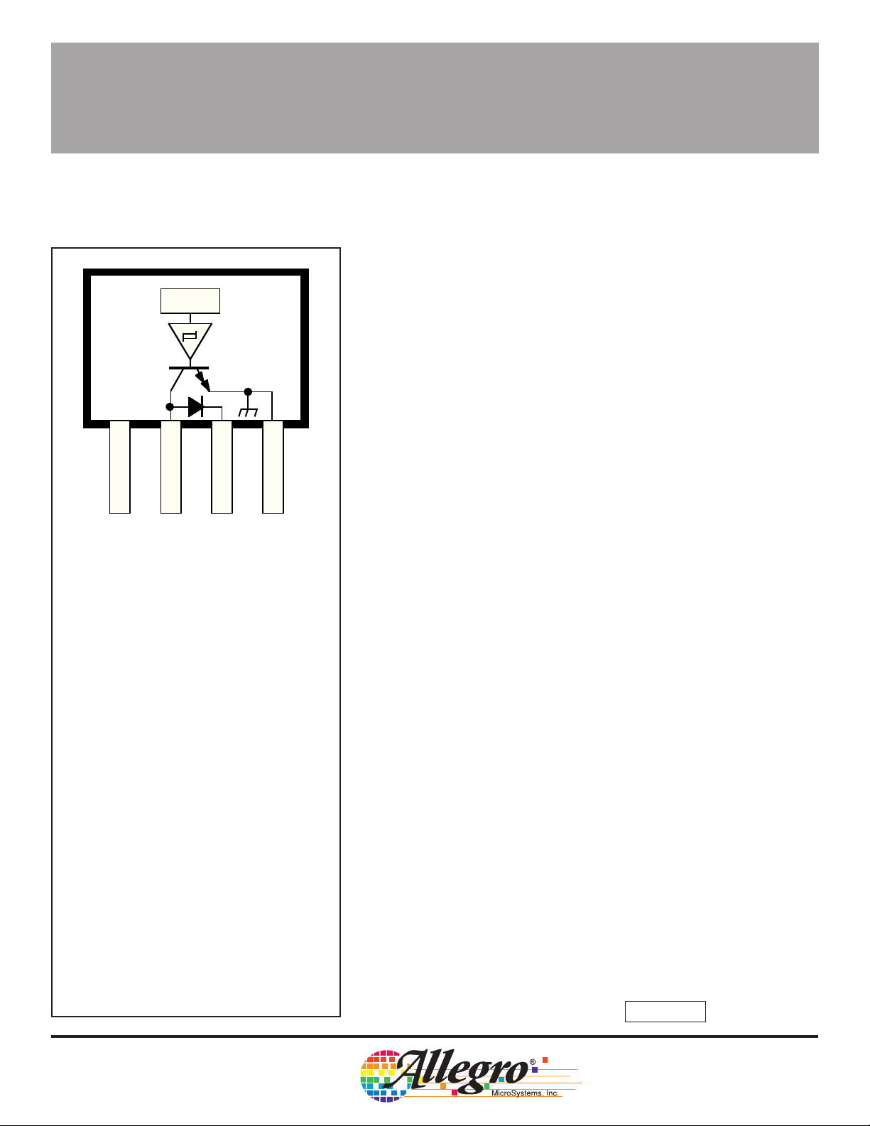
27695*
X
V
CC
1
Pinning is shown viewed from branded side.
234
SUPPLY
OUTPUT
DIODE
GROUND
Dwg. PH-001
ABSOLUTE MAXIMUM RATINGS
at T
= +25°C
A
PROTECTED POWERHALL
®
SENSOR
— LAMP/SOLENOID DRIVER
The UGQ5140K unipolar Hall effect switch is a monolithic
integrated circuit designed for magnetic actuation of low-power
incandescent lamps or inductive loads such as relays or solenoids.
Included on chip is a Darlington power output that is capable of continuously sinking in excess of 300 mA. Internal protection circuitry
limits surge (lamp turn-ON) or fault currents to approximately 900 mA.
A sensitive magnetic threshold allows the device to be used in conjunction with inexpensive magnets or in applications that require
relatively large operating distances.
Each sensor/driver includes a magnetic sensing Hall voltage
generator, operational amplifier, Schmitt trigger, voltage regulator, and
an open-collector, high-gain Darlington power output stage. The
regulator allows use of the device with supply voltages of 4.5 V to
28 V. On-chip compensation circuitry stabilizes switch-point performance over temperature. The magnetic operation of this device is
similar to that of the A3141E— Hall-effect switch.
The sensitive magnetic switch point coupled with the power output,
current limiting, and thermal limiting circuitry allow the UGQ5140K to
magnetically actuate various loads without requiring any external
components.
The UGQ5140K is rated for operation over an extended temperature range of -40°C to +85°C. It is supplied in a four-pin mini-SIP
plastic package, 0.200" (5.08 mm) wide, 0.130" (3.30 mm) high, and
0.060" (1.54 mm) thick.
Supply Voltage, VCC . . . . . . . . . . . . . . 28 V
Reverse Battery Voltage, V
Output OFF Voltage, V
Over-Current Protected Output Voltage,
V
. . . . . . . . . . . . . . . . . . . . . . . . 25 V
OUT
Output ON Current, I
Magnetic Flux Density, B . . . . . . Unlimited
Package Power Dissipation,
P
.. . . . . . . . . . . . . . . . . . . See Graph
D
Operating Temperature Range,
T
. . . . . . . . . . . . . . . . . -40°C to +85°C
A
Storage Temperature Range,
T
. . . . . . . . . . . . . . . . -65°C to +150°C
S
* Output is current limited at approximately 900
mA and junction temperature limited if current in
excess of 900 mA is attempted. See Circuit
Description and Applications for further
information.
OUT
OUT
. . . . . -45 V
RCC
. . . . . . . . . . 45 V
. . . . . . . 900 mA*
FEATURES
■ Magnetically Actuated Power Switch
■ Temperature-Compensated Switch Points
■ High Current-Sink Capability
300 mA Continuous
900 mA Peak Current Limit
■ Output Short-Circuit Protection
■ Low Quiescent Standby Current
■ Linear Thermal Limiting
■ Automotive Temperature Range
-40°C to +85°C, Operating
■ Internal Inductive Flyback/Clamp Diode Protection
■ Reverse Battery Protection
■ Low-Profile 4-Pin Mini-SIP
Always order by complete part number: UGQ5140K .
Page 2
5140
ALLOWABLE PACKAGE POWER DISSIPATION IN WATTS
1
3
2
4
PROTECTED POWERHALL
®
SENSOR:
LAMP/SOLENOID DRIVER
FUNCTIONAL BLOCK DIAGRAM
V
CC
REV. BATTERY
PROTECTION
REG.
X
THERMAL
LIMIT
CURRENT
LIMIT
ELECTRICAL CHARACTERISTICS at T
DIODE
OUTPUT
<<1Ω
GROUND
Dwg. FH-001
= -40°C to +85°C, V
A
1.0
0.8
0.6
0.4
0.2
0
-50
= 4.5 V to 24 V
CC
FREE AIR, R = 177°C/W
θJA
25
0-25
AMBIENT TEMPERATURE IN °C
50 75 100 125 150
(unless otherwise noted).
Limits
Characteristic Symbol Test Conditions Min. Typ. Max. Units
Supply Voltage Range V
Output Leakage Current I
Output Sustaining Voltage V
Output Saturation Voltage V
OUT(SUS)
OUT(SAT)
Over-Current Limit I
Output Rise Time t
Output Fall Time t
Supply Current I
Diode Forward Voltage V
Diode Leakage Current I
Thermal Limit T
CC
OUT
LIMIT
r
f
CC
F
R
LIMIT
Operating 4.5 12 24 V
V
= 24 V — <1.0 10 µA
OUT
I
= 100 mA 35 — — V
OUT
I
= 300 mA, VCC = 24 V — 0.84 1.2 V
OUT
VCC = V
= 12 V, B ≥ 500 G — 900 — mA
OUT
VCC = 12 V, VBB = 18 V, — 0.04 2.0 µs
RL = 1.1 kΩ, CL = 20 pF — 0.04 2.0 µs
Output OFF — 5.5 10 mA
IF = 300 mA — 1.1 1.5 V
VR = 35 V — <1.0 50 µA
VCC = V
I
OUT
= 12 V, B ≥ 500 G,
OUT
= 10 mA — 165 — °C
Dwg. GH-001
Typical Data is at TA = +25°C and is for design information only.
MAGNETIC CHARACTERISTICS at VCC = 4.5 V to 24 V.
Characteristic Symbol Min. Typ. Max. Min. Typ. Max. Units
Magnetic Operate Point B
Magnetic Release point B
Hysteresis B
OP
RP
hys
TA = +25°CT
= -40°C to +85°C
A
70 155 200 45 — 240 G
50 100 180 25 — 220 G
20 55 — 20 — — G
115 Northeast Cutoff, Box 15036
Worcester, Massachusetts 01615-0036 (508) 853-5000
W
Copyright © 1991, 1995 Allegro MicroSystems, Inc.
Page 3
5140
PROTECTED POWERHALL
®
SENSOR:
LAMP/SOLENOID DRIVER
TYPICAL OPERATING CHARACTERISTICS
1000
950
900
850
PEAK CURRENT LIMIT IN mA
800
750
-20-40
0
AMBIENT TEMPERATURE IN °C
25 85 105 125
55
Dwg. GH-004
1.0
0.9
0.8
0.7
SATURATION VOLTAGE IN VOLTS
0.6
-40
-20 0 25 55
AMBIENT TEMPERATURE IN °C
I = 300 mA
OUT
Dwg. GH-002A
85
180
160
OPERATE POINT
140
120
SWITCH POINT IN GAUSS
100
80
-40
-20 0 25 55
AMBIENT TEMPERATURE IN °C
I = 10 mA
OUT
RELEASE POINT
85
Dwg. GH-006A
9.0
8.0
7.0
6.0
SUPPLY CURRENT IN mA
5.0
-40
-20 0 25 55
AMBIENT TEMPERATURE IN °C
OUTPUT ON
I = 10 mA
OUT
OUTPUT OFF
V = 12 V
CC
85
Dwg. GH-003A
Page 4

5140
PROTECTED POWERHALL
®
SENSOR:
LAMP/SOLENOID DRIVER
TYPICAL TRANSFER CHARACTERISTICS
at T
= +25°C
A
15
12
9.0
6.0
3.0
OUTPUT VOLTAGE IN VOLTS
V
B B
I = 300 mA
OUT
B
RP
V
0
MAGNETIC FLUX DENSITY IN GAUSS
75
50250
OUT(SAT)
100 125 150 175 200
B
OP
Dwg. GH-007
CIRCUIT DESCRIPTION AND OP-
ERATION
The UGQ5140K merges state-of-the-art
Hall effect sensing and power driving technologies to allow precision non-contact
actuation of incandescent lamps or inductive
loads. It is rated for operation over an
extended temperature range as typically
required in automotive applications.
MAGNETIC OPERATION
As shown in the Transfer Characteristics
graph, the output of the device (pin 2)
switches low when the magnetic field at the
Hall sensor exceeds the operate point
threshold (BOP). At this point, the output
voltage is V
OUT(SAT)
is reduced to below the release point threshold (BRP), the device output goes high. The
difference in the magnetic operate and
release points is called the hysteresis (BH) of
the part. This built-in hysteresis allows clean
switching of the output even in the presence
of external mechanical vibration and electrical noise.
. When the magnetic field
CURRENT AND THERMAL
LIMITING
Output short circuits may be caused by
faulty connectors, crimped wiring harnesses,
or blown loads. In such cases, current and
thermal limit circuitry will protect the output
transistor against destruction.
Current through the output transistor is
sensed with a low-value on-chip aluminum
resistor. The voltage drop across this
resistor is fed back to control the base drive
of the output stage. This feedback prevents
the output transistor from exceeding its
maximum current density rating by limiting
the output current to approximately 900 mA.
It may also cause the output voltage to
increase (V
mode, the device will dissipate an increased
amount of power (PD = V
output transistor will be thermally stressed.
= VBB - [I
OUT
x RL]). In this
LIMIT
x I
OUT
LIMIT
) and the
115 Northeast Cutoff, Box 15036
Worcester, Massachusetts 01615-0036 (508) 853-5000
Page 5

5140
PROTECTED POWERHALL
®
SENSOR:
LAMP/SOLENOID DRIVER
This stress, unless protected against (as in the
UGQ5140K), will cause the device junction temperature to rise until it fails catastrophically.
Thermal stress protection is provided in two
manners; delta temperature protection, and junction
temperature protection. Under worst-case conditions
(see Figures 1 and 2), if the output is shorted to
supply, the output transistor will heat up much faster
than the rest of the integrated circuit. This condition
could cause localized failure in the output transistor.
To prevent damage, a delta temperature limiting
scheme is used. If a large thermal gradient is sensed
across the device, the output transistor base drive is
reduced to lower the output current. This reduces the
power (heat) generated by the output transistor.
When thermal stresses cause the junction temperature to reach approximately +165°C, a linear
thermal limiting circuit is activated. This circuit linearly
reduces the base drive of the output transistor to
maintain a constant junction temperature of 165°C. In
this mode, the output current will be a function of the
heat dissipating characteristics of the package and its
environment. Linear thermal limiting eliminates the
low-frequency thermal oscillation problems experienced by thermal shutdown (ON-OFF) schemes.
FIGURE 1
OUTPUT CURRENT UNDER SHORT-CIRCUIT
CONDITIONS
NOT TO SCALE
PEAK CURRENT LIMIT
DELTA TEMP.
LIMIT
OUTPUT CURRENT
TIME
JUNCTION
TEMP. LIMIT
FIGURE 2
OUTPUT VOLTAGE vs OUTPUT CURRENT
Dwg. WH-002
The output characteristics are shown in Figures 1
and 2. Note the three distinct operating regions: peak
limit, delta limit, and thermal limit. In practice the
output voltage and current may exhibit some oscillations during peak current limiting due to output load
characteristics. These oscillations are of very-short
duration (typically 50 ms) and may be damped with an
external capacitor between pins 2 and 4.
When the fault condition that caused the output
overload is corrected, the device returns to normal
operating mode.
OUT
T = 165°C
J
JUNCTION
OUTPUT VOLTAGE, V
TEMP. LIMIT
T < 150°C
J
V
OUT(SAT)
OUTPUT CURRENT, I
DELTA
TEMP. LIMIT
NOT TO SCALE
CURRENT LIMIT
OUT
Dwg. GP-013-1
Page 6

5140
PROTECTED POWERHALL
®
SENSOR:
LAMP/SOLENOID DRIVER
FIGURE 3
TYPICAL LAMP DRIVER APPLICATION
X
V
+12 V
CC
1
OPTIONAL LAMP TEST
(SEE TEXT)
432
Dwg. EH-001
FIGURE 4
LAMP CURRENT vs TIME
NORMAL LAMP IN-RUSH CURRENT
TYPICAL APPLICATIONS
INCANDESCENT LAMP DRIVER
High incandescent lamp turn-ON currents (commonly called in-rush currents) can contribute to poor lamp
reliability and destroy semiconductor lamp drivers. Warming resistors protect both driver and lamp but use significant power when the lamp is OFF while current-limiting
resistors waste power when the lamp is ON. Lamps with
steady-state current ratings to 300 mA can be driven by
the UGQ5140K (Figure 3) without the need for warming or
current limiting resistors. In applications using several
sensor/drivers to control multiple lamps, the internal clamp
diodes may be connected together to an appropriate
current-limiting resistor and simple “lamp test” switch.
As shown in Figure 4, when an incandescent lamp is
initially turned ON, the cold filament is at minimum resistance and will normally allow a 10x to12x peak in-rush
current. As the lamp warms up, the filament resistance
increases to its rated value and the lamp current is
reduced to its steady-state rating. When switching a lamp
with the UGQ5140K, the internal current-limiting circuitry
limits the peak current to approximately 900 mA. The
device will stay in the current limit and delta temperature
limit modes until the lamp resistance increases to its rated
steady-state value (Figure 4). A side-effect of this currentlimiting feature is that lamp turn-on times will increase.
Typical lamp turn-on times are shown in Figure 5.
CURRENT LIMIT
DELTA TEMP.
LIMIT
TIME
NOT TO SCALE
INDUCTIVE LOAD DRIVER
Connecting the internal clamp diode (pin 3) to the
positive supply allows relays or other inductive loads to be
driven directly, as shown in Figure 6. The internal diode
prevents damage to the output transistor by clamping the
high-voltage spikes which occur when turning OFF an
inductive load. An optional external Zener diode can be
used to increase the flyback voltage, providing a much
faster inductive load turn-OFF current decay, resulting in
faster dropout (reduced relay contact arcing), and improved performance. The maximum Zener voltage, plus
the load supply voltage, plus the clamp diode forward
voltage should not exceed 35 volts.
-
115 Northeast Cutoff, Box 15036
Worcester, Massachusetts 01615-0036 (508) 853-5000
Page 7

5140
A
PROTECTED POWERHALL
®
SENSOR:
LAMP/SOLENOID DRIVER
FIGURE 5
LAMP TURN-ON TIME
150
125
#168 BULB
100
75
#194 BULB
14 V, 270 mA
50
APPROXIMATE LAMP TURN-ON TIME IN ms
25
-40
-20 0 25 55
AMBIENT TEMPERATURE IN °C
14 V, 350 mA
TYPICAL RELAY/SOLENOID DRIVER APPLICATION
V = 14 V
BB
85
Dwg. GH-005A
FIGURE 6
SENSOR LOCATION
ACTIVE AREA DEPTH
0.015"
0.38 mm
NOM
BRANDED
SURFACE
0.121"
3.07 mm
0.053"
1.34 mm
1 432
Dwg. MH-001B
+12 V
X
V
CC
1
OPTIONAL ZENER
432
Dwg. EH-002
V
OUTPUT
VOLTAGE
OUTPUT
CURRENT
BB
V
OUT(SAT)
V + V + V
BB Z F
ZENER CLAMP
V + V
BB F
DIODE CLAMP
Dwg. WP-001-1
Page 8

5140
PROTECTED POWERHALL
®
SENSOR:
LAMP/SOLENOID DRIVER
Dimensions in Inches
(controlling dimensions)
0.208
0.203
45°
0.138
0.133
0.085
1234
MAX
0.600
0.560
0.063
0.059
0.033
0.015
45°
Dimensions in Millimeters
(for reference only
5.28
5.16
45°
3.51
3.38
2.16
1234
MAX
15.24
14.23
1.60
1.50
45°
0.84
0.38
SEE NOTE
0.016
NOTES: 1. Tolerances on package height and width represent allowable mold offsets. Dimensions given are measured at the widest point (parting line).
2. Exact body and lead configuration at vendor’s option within limits shown.
3. Height does not include mold gate flash.
4. Recommended minimum PWB hole diameter to clear transition area is 0.035” (0.89 mm).
5. Where no tolerance is specified, dimension is nominal.
0.050
BSC
Dwg. MH-009C in
Allegro MicroSystems, Inc. reserves the right to make, from time to time, such departures from
the detail specifications as may be required to permit improvements in the design of its products.
The information included herein is believed to be accurate and reliable. However, Allegro
MicroSystems, Inc. assumes no responsibility for its use; nor for any infringements of patents or
other rights of third parties which may result from its use.
SEE NOTE
0.41
1.27
BSC
Dwg. MH-009C mm
115 Northeast Cutoff, Box 15036
Worcester, Massachusetts 01615-0036 (508) 853-5000
 Loading...