

Page 1
Quick Start Guide
V
V
UG-378
One Technology Way • P. O . Box 9106 • Norwood, MA 02062-9106, U.S.A. • Tel : 781.329.4700 • Fax : 781.461.3113 • www.analog.com
Overview of AD5110/AD5112/AD5114 Connections and Functionality
GENERAL DESCRIPTION
This quick start guide provides a general overview of AD5110/
AD5112/AD5114 connections and functionality and should be
reviewed in conjunction with the AD5110/AD5112/AD5114
data sheet.
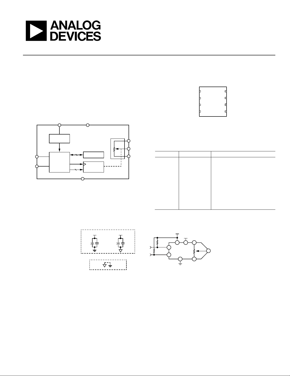
FUNCTIONAL BLOCK DIAGRAM
LOGIC
POWER-ON
RESET
SDA
SCL
2
I
SERIAL
INTERFACE
DATA
C
DATA
DD
AD5110/AD5112/AD5114
EEPROM
RDAC
REGISTER
GND
Figure 1.
TYPICAL EXTERNAL CONNECTIONS
SUPPLIES
V
DD
++
GROUNDS
DIGITAL
GND
V
LOGIC
ANALOG
GND
A
W
B
0.1µF0.1µF10µF 10µF
10547-001
SCL
SDA
Figure 3.
PIN CONFIGURATION
1V
DD
NOTES
1. THE EXPOSED PAD IS INTERNALLY FLOATING.
2A
3W
4B
AD5110/
AD5112/
AD5114
TOP VIEW
(Not to Scale)
Figure 2.
8V
LOGIC
7SDA
6SCL
5GND
PIN FUNCTION DESCRIPTIONS
Table 1.
Pin No. Mnemonic Description
1 VDD Positive power supply.
2 A Terminal A of RDAC.
3 W Wiper terminal of RDAC.
4 B Terminal B of RDAC.
5 GND Ground pin.
6 SCL Serial clock line.
7 SDA Serial data line.
8 V
EPAD Internally floating exposed pad.
V
LOGIC
2.2kΩ
6
2.2kΩ
7
Logic power supply.
LOGI C
V
DD
A
2
18
3
w
4
5
B
10547-003
10547-002
PLEASE SEE THE LAST PAGE FOR AN IMPORTANT
WARNING AND LEGAL TERMS AND CONDITIONS.
Rev. 0 | Page 1 of 4
Page 2

UG-378 Quick Start Guide
OPERATIONAL CONDITIONS
Table 2. Specifications
Parameter Specification
VDD to GND 2.3 V to 5.5 V
V
to GND 1.8 V to VDD
LOGI C
VA, VW, VB to GND GND to VDD
Maximum Continuous IA, IW, IB
RAW = 5 kΩ and 10 kΩ ±6 mA
RAW = 80 kΩ ±1.5 mA
Maximum Clock (SCL) 400 kHz
Table 3. Device Address Selection
Model 7-Bit I2C Device Address
AD511X1 BCPZ Y2 0101111
AD511X1 BCPZ Y2-1 0101100
1
Model.
2
Resistance.
SHIFT REGISTER AND TIMING DIAGRAM
191 9 91
SCL
SDA
START BY
MASTER
111A1A0 C2C1
FRAME 1
SERIAL BUS ADDRESS BYTE
R/W0 000000
ACK. BY
AD5110
MOST SIGNIFICANT DATA BYTE
FRAME 2
C0 D7 D6 D5 D4 D3 D2 D1 D0
ACK. BY
AD5110
LEAST SIGNIFICANT DATA BYTE
FRAME 3
ACK. BY STOP BY
AD5110 MASTER
Figure 4. Write Sequence
COMMANDS
Table 4. Command Operation Truth Table
Command Data
Command
Number
DB10 DB8 DB7 DB0
C2 C1 C0 D7 D6 D5 D4 D3 D2 D1 D0
0 0 0 0 X X X X X X X X No operation
1 0 0 1 X X X X X X X X Write contents of RDAC register to EEPROM
2 0 1 0 0
6
5 4 3 2 1
MSB
1 0 0 0 0 0 0 0 Top scale
1 1 1 1 1 1 1 1 Bottom scale
3 0 1 1 X X X X X X X A0 Software shutdown
4 1 0 0 X X X X X X X X Software reset: refresh RDAC register with EEPROM
5 1 0 1 X X X X X X X X Read contents of RDAC register
6 1 1 0 X X X X X X A1 A0 Read contents of EEPROM
1
X is a don’t care.
2
In the AD5114, this bit is a don’t care.
3
In the AD5112, this bit is a don’t care.
1
Operation
2
2, 3
Write contents of serial register data to RDAC
0
LSB
Shutdown off
Shutdown on
A1 A0 Data
0 0 Wiper position saved
0 1 Resistor tolerance
10547-004
Rev. 0 | Page 2 of 4
Page 3

Quick Start Guide UG-378
HOW TO CALCU L ATE THE ACTUAL END-TO-END RESISTANCE
For example, if RAB = 10 kΩ and the resistor tolerance data readback shows 01010010 (see Table 5), the end-to-end resistance can be
calculated as:
DB[7]: 0 = negative (1 = positive)
DB[6:3]: 1010 = 10
DB[2:0]: 010 = 2 × 2
Then:
Tolerance = −10.25% and, therefore, R
Table 5. Resistor Tolerance Format
DB7 DB6 DB5 DB4 DB3 DB2 DB1 DB0
Sign 24 23 22 2 . 2−1 2−2 2−3
EXAMPLES
Table 6. Write the RDAC Register and Place the Wiper at Zero Scale
Sequence I2C Address Write RDAC Command Zero Scale
Data 0x5E 0x02 0x00
−3
= 0.25
= 8.975 kΩ.
AB
Data Byte
Table 7. Readback the Wiper Position Saved
Sequence I2C Address Write EEPROM Readback Command Location I2C Address Readback Data
Data 0x5E 0x06 0x00 Repeat start 0x5F 0xXX
Rev. 0 | Page 3 of 4
Page 4

UG-378 Quick Start Guide
and between you (“Customer”) and Analog Devices, Inc.
S BE LIABLE FOR ANY INCIDENTAL, SPECIAL, INDIRECT, OR CONSEQUENTIAL DAMAGES RESULTING FROM CUSTOMER’S POSSESSION OR USE OF
accordance with the substantive laws of the Commonwealth of
NOTES
REVISION HISTORY
3/12—Revision 0: Initial Version
ESD Caution
ESD (electrostatic discharge) sensitive device. Charged devices and circuit boards can discharge without detection. Although this product features patented or proprietary protection
circuitry, damage may occur on devices subjected to high e nergy ESD. Therefore, proper ES D precautions should be taken t o avoid performance degradation or loss of functionality.
Legal Terms and Conditions
By using the evaluation board discussed herein (together with any tools, components documentation or support materials, the “Evaluation Board”), you are agreeing to be bound by the terms and conditions
set forth below (“Agreement”) unless you have purchased the Evaluation Board, in which case the Analog Devices Standard Terms and Conditions of Sale shall govern. Do not use t he Evaluation Board until you
have read and agreed to the Agreement. Your use of the Evaluation Board shall signify your acceptance of the Agreement. This Agreement is made by
(“ADI”), with its principal place of business at One Technology Way, Norwood, MA 02062, USA. Subject to the terms and conditions of the Agreement, ADI hereby grants to Customer a free, limited, personal,
temporary, non-exclusive, non-sublicensable, non-transferable license to use the Evaluation Board FOR EVALUATION PURPOSES ONLY. Customer understands and agrees that the Evaluation Board is provided
for the sole and exclusive purpose referenced above, and agrees not to use the Evaluation Board for any other purpose. Furthermore, the license granted is expressly made subjec t to the following additional
limitations: Customer shall not (i) rent, lease, display, sell, transfer, assign, sublicense, or distribute the Evaluation Board; and (ii) permit any Third Party to access the Evaluation Board. As used herein, the term
“Third Party” includes any entity other than ADI, Customer, their employees, affiliates and in-house consultants. The Evaluation Board is NOT sold to Customer; all rights not expressly granted herein, including
ownership of t he Evaluation Board, are res erved by ADI. CONFIDENTIA LITY. This Agreement and the Evaluation Board shall all be considered the confidential a nd proprietary information o f ADI. Customer may
not disclose or transfer any portion of the Evaluation Board to any other party for any reason. Upon discontinuation of use of the Evaluation Board or termination of this Agreement, Customer agrees to
promptly return the Evaluation Board to ADI. ADDITIONAL RESTRICTIONS. Customer may not disassemble, decompile or reverse engineer chips on the Evaluation Board. Customer shall inform ADI of any
occurred damages or any modifications or alterations it makes to the Evaluation Board, including but not limited to soldering or any other activity that affects the material content of the Evaluation Board.
Modifications to the Evaluation Board must comply wi th applicable law, including but not limited to the RoHS Directive. TERMINATION. ADI may terminate this Agreement at any time upon giving written notice
to Customer. Customer agrees to return to ADI the Evaluation Board at that time. LIMITATION OF LIABILITY. THE EVALUATION BOARD PROVIDED HEREUNDER IS PROVIDED “AS IS” AND ADI MAKES NO
WARRANTIES OR REPRES ENTATIONS OF ANY KIND WITH RESPECT TO IT. ADI SPECIFICALLY DISCLAIMS ANY REPRESENTATIONS, END ORSEMENTS, GUARANTEES, OR WARRANTIES, EXPRESS OR IMPLIED, RELATED
TO THE EVALUATION BOARD INCLUDING, BUT NOT LIMITED TO, THE IMPLIED WARRANTY OF MERCHANTABILITY, TITLE, FITNESS FOR A PARTICULAR PURPOSE OR NONINFRINGEMENT OF INTELLECTUAL
PROPERTY RIGHTS. IN NO EVENT WILL ADI AND ITS LICENSOR
THE EVALUATION BOARD, INCLUDING BUT NOT LIMITED TO LOST PROFITS, D ELAY COSTS, LAB OR COSTS OR LOSS OF GOODWILL. ADI’S TOTAL LIABILIT Y FROM ANY AND ALL CAUSES SHALL BE LIMITED TO THE
AMOUNT OF ONE HUNDRED US DOLLARS ($100.00). EXPORT. Customer agrees that it will not directly or indirectly export the Evaluation Board to another country, and that it will comply with all applicable
United States federal laws and regulations relating to exports. GOVERNING LAW. This Agreement shall be governed by and construed in
Massachusetts (excluding conflict of law rules). Any legal action regarding this Agreement will be heard in the state or federal courts having jurisdiction in Suffolk County, Massachusetts, and Customer h ereby
submits to the personal jurisdiction and venue of such courts. The United Nations Convention on Contracts for the International Sale of Goods shall not apply to this Agreement and i s expressly disclai med.
©2012 Analog Devices, Inc. All rights reserved. Trademarks and
registered trademarks are the property of their respective owners.
UG10547-0-3/12(0)
Rev. 0 | Page 4 of 4
 Loading...