

Page 1
Evaluation Board User Guide
p
UG-364
One Technology Way • P. O . Box 9106 • Norwood, MA 02062-9106, U.S.A. • Tel : 781.329.4700 • Fax : 781.461.3113 • www.analog.com
Evaluating the AD5933 1 MSPS, 12-Bit Impedance Converter Network Analyzer
FEATURES
Full-featured evaluation board for the AD5933
Graphic user interface software with frequency sweep
capability for board control and data analysis
Various power supply linking options
Standalone capability with serial I
2
C loading from on-board
microcontroller
Selectable system clock options including internal RC
oscillator or on-board 16 MHz crystal
APPLICATIONS
Electrochemical analysis
Impedance spectroscopy
Complex impedance measurement
Corrosion monitoring and protection equipment
Biomedical and automotive sensors
Proximity sensing
GENERAL DESCRIPTION
This user guide describes the EVAL-AD5933EBZ evaluation board,
and the application software developed to interface with the device.
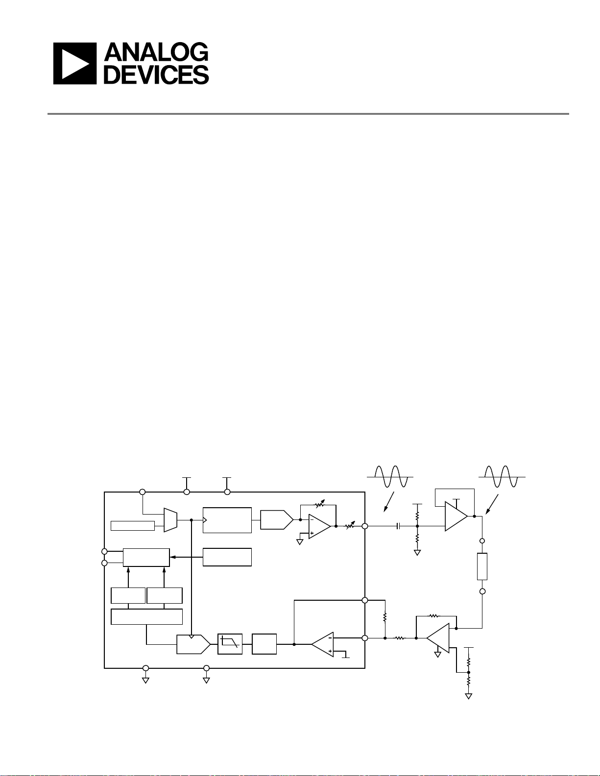
The AD5933 is a high precision impedance converter system that
combines an on-board frequency generator with a 12-bit, 1 MSPS
analog-to-digital converter (ADC). The frequency generator
allows an external complex impedance to be excited with a
EVALUATION BOARD BLOCK DIAGRAM
V
DD
MCLK
OSCILLATOR
SCL
SDA
PLEASE SEE THE LAST PAGE FOR AN IMPORTANT
WARNING AND LEGAL TERMS AND CONDITIONS.
I2C
INTERFACE
IMAGINARY
REAL
REGISTER
REGISTER
1024-POINT DFT
AGND DGND
ADC
(12 BITS)
Rev. 0 | Page 1 of 28
V
DD
DVDDAVD D
DDS
CORE
(27 BITS)
TEMPERATURE
SENSOR
AD5933
LPF
DAC
GAIN
OUTPUT AMPLIFIER
Figure 1.
known frequency. The on-board ADC samples the response
signal from the impedance, and an on-board DSP engine at each
excitation frequency processes the DFT. The AD5933 also contains
an internal temperature sensor with 13-bit resolution. The part
operates from a 2.7 V to 5.5 V supply. Other on-board components
include a ADR423 3.0 V reference to act as a stable supply voltage
for the separate analog and digital sections of the device and a
ADP3303 ultrahigh precision regulator to act as a supply to the
on-board universal serial bus controller that interfaces to the
AD5933. The user has the option to power the entire circuitry
from the USB port of a computer.
The evaluation board also has a high performance trimmed
16 MHz surface-mount crystal to act as a system clock to the
AD5933, if required. The various link options located around the
evaluation board are listed in Table 1 . Interfacing to the AD5933
is through a USB microcontroller that generates the I
necessary to communicate with the AD5933. Interfacing to the
USB microcontroller is done through a Visual Basic® graphic user
interface located on and run from the PC. Complete specifications
for the AD5933 are available in the AD5933 data sheet available
from Analog Devices, Inc., and should be consulted in conjunction
with this user guide when using the evaluation board.
TRANSMIT SI DE
I-V
R
VDD/2
1.48V
OUT
1.98V p-p
VOUT
RFB
VIN
47nF
20kΩ
20kΩ
V
DD
50kΩ
50kΩ
A1, A2 ARE
½
AD8606
V
DD
−
A1
+
R
FB
−
A2
+
VDD/2
V
DD
50kΩ
50kΩ
1.98V p-
Z
UNKNOWN
2
C signals
10441-001
Page 2

UG-364 Evaluation Board User Guide
TABLE OF CONTENTS
Features.............................................................................................. 1
Applications....................................................................................... 1
General Description ......................................................................... 1
Evaluation Board Block Diagram................................................... 1
Revision History ............................................................................... 2
Evaluation Board Hardware............................................................ 3
Terminal Block Functions ........................................................... 3
Getting Started.................................................................................. 4
Setup Sequence Summary........................................................... 4
Installing the Software ................................................................. 4
Connecting the USB Cable.......................................................... 5
Verifying the Links and Power Up the Evaluation Board ....... 6
REVISION HISTORY
2/12—Revision 0: Initial Version
Performing a Frequency Sweep ...................................................6
Two Installation Frequently Asked Questions ....................... 10
Source Code for Impedance Sweep.............................................. 12
Evaluation Board Source Code Extract................................... 13
Gain Factor Calculation ............................................................ 17
Temperature Measurement ....................................................... 17
Impedance Measurement Tips ................................................. 18
Evaluation Board Schematics and Artwork................................ 23
Ordering Information.................................................................... 26
Bill of Materials........................................................................... 26
Related Links............................................................................... 27
Rev. 0 | Page 2 of 28
Page 3

Evaluation Board User Guide UG-364
EVALUATION BOARD HARDWARE
TERMINAL BLOCK FUNCTIONS
Table 1. Link Functions
Link No. Default Location Function
LK1 Out Option to remove external conditioning
LK2 Out Option to remove external conditioning
LK3 In On-board, 16 MHz crystal connection, connects to Y2
LK4 Out SMB connected external clock
LK5 In Connects 5 V from USB to ADP3303
LK6 A AVDD and DVDD power supply connector
Rev. 0 | Page 3 of 28
Page 4
UG-364 Evaluation Board User Guide
GETTING STARTED
SETUP SEQUENCE SUMMARY
The evaluation board installation instructions are for the
Windows XP® operating system with English (United States) set
for its language. The regional and language settings of a PC can
be changed in the Regional and Language directory within the
Control Panel (Start/Control Panel/Regional and Language/
Formats). The installation consists of the following steps that
are described in detail in the sections that follow.
1. Install the AD5933 graphical user interface software on the
CD that accompanies the evaluation board. Do not connect
the USB cable from the AD5933 evaluation board to the
computer USB hub until the evaluation software is properly
installed. See the Installing the Software section for
additional information.
2. Connect the computer USB port to the evaluation board
using the USB cable provided in the evaluation kit and run
the USB hardware installation wizard after the evaluation
software is correctly installed (the hardware installation
may happen automatically depending on the settings of the
current operating system). See the Connecting the USB
Cable section for additional information.
3. Ensure that the appropriate links are made throughout
the evaluation board. Prior to opening and running the
evaluation software program, power up the evaluation
board appropriately. See the Verifying the Links and Power
Up section for additional information.
4. Configure the front panel of the evaluation board software to
run the required sweep function. See the Performing a
Frequency Sweep section for additional information.
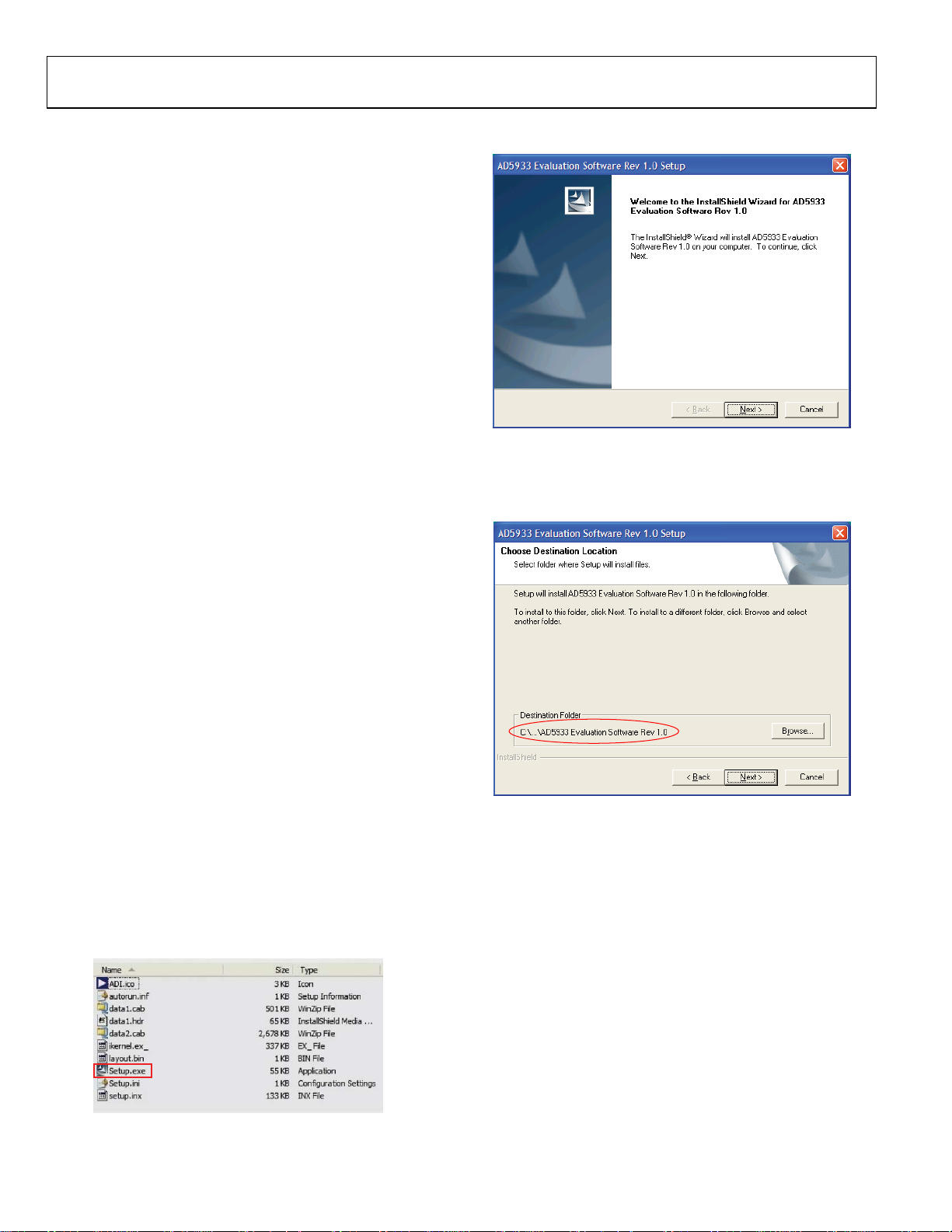
3. Install the evaluation board software in the default destination
folder path, C:\Program Files\Analog Devices\AD5933\
AD5933 Evaluation Software Rev 1.0 Setup (see Figure 4).
Figure 3. Installation Wizard
10441-004
INSTALLING THE SOFTWARE
To install the evaluation board software, use the following steps:
1. Put the evaluation board CD into the CD drive of the PC
and click Start/My Computer.
2. The CD software installation may happen automatically
after the CD is inserted into the CD drive; however, this may
depend on the settings of the current operating system. If the
software installation does not automatically start, go to
AD5933 Installation/Setup.exe and double-click Setup.exe
to install the software on the PC through the installation
wizard (see Figure 2 and Figure 3).
10441-003
Figure 2. Evaluation Software CD Contents
Rev. 0 | Page 4 of 28
10441-005
Figure 4. Default Destination Folder
Page 5
Evaluation Board User Guide UG-364
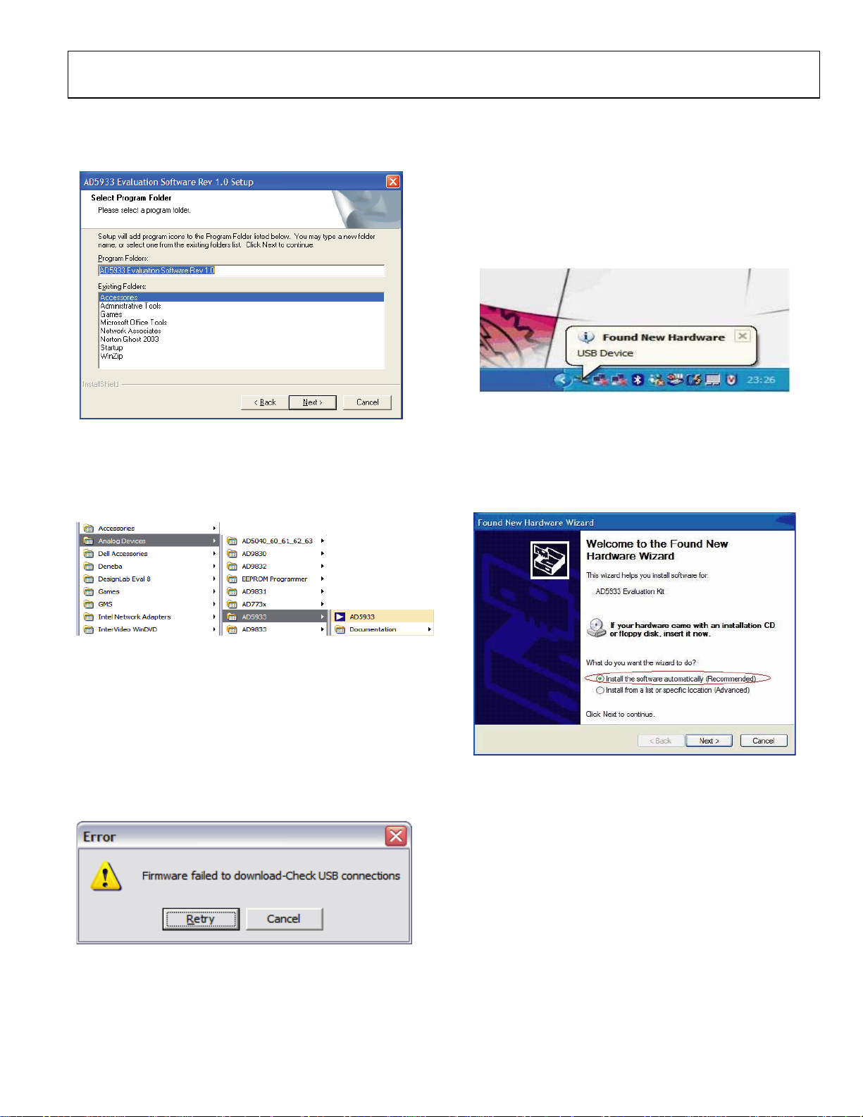
4. Choose the Analog Devices directory (see Figure 5). If the
Analog Devices folder does not yet exist, create an Analog
Devices folder and add the program icon to this new folder.
Figure 5. Select Analog Devices Directory
5. After installing the software, remove the CD from the CD
drive. You may be asked to reboot the computer at this stage.
6. Go to Start/All Programs/Analog Devices/AD5933/
AD5933 (see Figure 6).
10441-006
CONNECTING THE USB CABLE
To connect the USB cable, use the following steps:
1. Plug the USB cable into the USB hub of the PC and connect
the other end of the USB cable into the AD5933 evaluation
board USB socket (see J1 in Figure 32). A message may
appear that a USB device has been detected on the host
computer and that new hardware has been found (see
Figure 8).
10441-009
Figure 8. USB Device Detected by Host Computer
2. The Found New Hardware Wizard then appears (see
Figure 9). This wizard locates and installs the appropriate
driver files for the AD5933 evaluation kit in the operating
system registry. Select Install the software automatically
(Recommended) and click Next > to continue (see Figure 9).
Figure 6. Opening the Evaluation Software
The following message appears (see Figure 7) because the
firmware code that the evaluation software operates from,
and that needs to be downloaded to the evaluation board USB
microcontroller memory each time the interface software
program is opened, cannot be successfully downloaded to
the evaluation board. The error message is presented because
there is currently no USB connection between the computer
and the AD5933 evaluation board at this stage; therefore,
this error message is to be expected. Click Cancel.
Figure 7. Expected Error Message
10441-007
10441-008
Rev. 0 | Page 5 of 28
Figure 9. Hardware Installation Wizard
10441-010
Page 6
UG-364 Evaluation Board User Guide
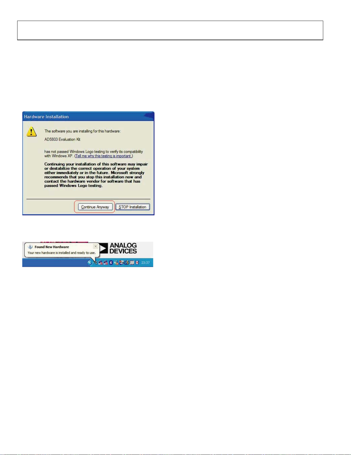
3. A standard windows operating system warning message
then appears, as shown in Figure 10. It indicates that the
new hardware currently being installing on the Windows®
operating system (AD5933 evaluation kit) has not passed the
Windows logo testing to verify compatibility with Windows
XP. This warning appears because the installation is an
evaluation setup installation and is not intended to be used
in a production environment. Click Continue Anyway and
then click Finish.
Figure 10. Expected Warning Message
The message shown in Figure 11 appears once the hardware has
been successfully installed.
Figure 11. Successful Hardware Installation
VERIFYING THE LINKS AND POWER UP THE EVALUATION BOARD
Ensure that the relevant links are in place on the evaluation board
(see Tabl e 1) and that the proper power connections and supply
values have been made to the terminal blocks before applying
power to the evaluation board. The power supply terminal blocks
are outlined in evaluation board schematic (see Figure 32). Note
that the USB connector only supplies power to the Cypress USB
controller chip that interfaces to the AD5933. If required, a
dedicated external voltage supply to each terminal block can
be provided. Ensure that all relevant power supply connections
and links are made before running the evaluation software. For
optimum performance, supply the three supply signals (A
A
VDD2
, and D
) from a stable external reference supply via the
VDD
power supply terminal blocks on the board.
,
VDD1
Rev. 0 | Page 6 of 28
10441-011
10441-012
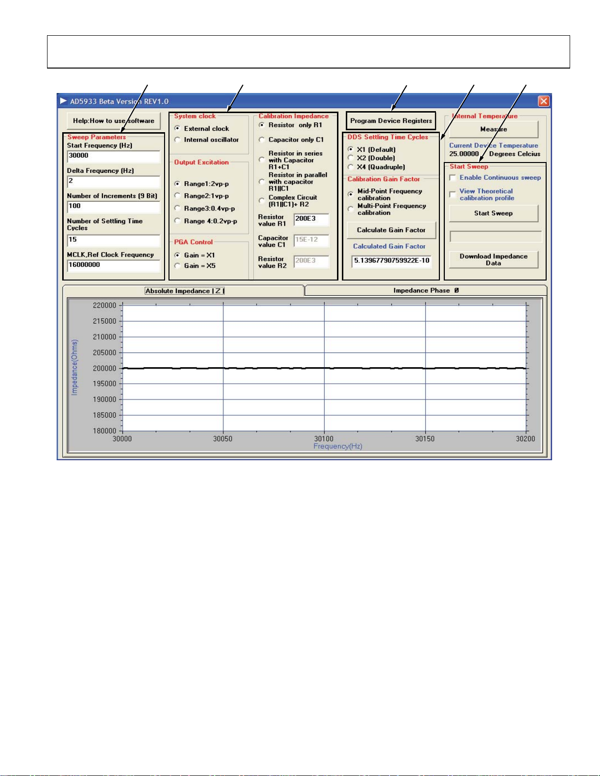
PERFORMING A FREQUENCY SWEEP
The sequence for performing a linear frequency sweep across a
200 k resistive impedance connected across the VOUT and
VIN pins within the frequency range of 30 kHz to 30.2 kHz is
outlined in this section. The default software settings for the
evaluation board are shown in Figure 12. (Note that a 200 k
resistor must be connected across the VIN and VOUT pins of
the AD5933). The default link positions are outlined in Tabl e 1,
see this before continuing.
To open the software, go to Start > Programs > Analog Devices >
AD5933 and click AD5933 Evaluation Software.
Figure 12 shows the graphic user interface program open and
running successfully. It also shows the interface panel along with
a frequency sweep impedance profile for a 200 k resistive
impedance (note R
To setup a typical sweep across a 200 k impedance (R
use the following steps:
• Set Start Frequency (Hz) to 30000 (Hz) within the Sweep
Parameters section (see 1 in Figure 12). The start frequency
is 24-bit accurate.
• Set Delta Frequency (Hz) to 2 (Hz) within the Sweep
Parameters section (see 1 in Figure 12). The frequency step
size is also 24-bit accurate.
• Set Number Increments (9 Bit) within the Sweep Parameters
section to 200 (see 1 in Figure 12) to set the number of
increments along the sweep to 200. The maximum number
of increments that the device can sweep across is 511, and
the value is stored in a register as a 9-bit value.
• Set Number of Settling Time Cycles to 15 (see 1 in Figure 12).
Note that when sweeping across a high-Q structure, such
as resonant impedance, users must ensure that the contents
of the settling time cycles register is sufficient to ensure
that the impedance under test settles before incrementing
between each successive frequency in the programmed
sweep. This is achieved by increasing the Number of
Settling Time Cycles value.
The delay between the time a frequency increment takes place
on the output of the internal direct digital synthesizer (DDS)
core and the time the ADC samples the response signal at
this new frequency is determined by the contents of the
number of settling time cycles registers (Register 0x8A and
Register 0x8B), see the AD5933 data sheet for further details.
For example, if a value of 15 is programmed into the Number
of Settling Time Cycles box, and if the next output frequency
is 32 kHz, the delay between the time the DDS core starts
to output the 32 kHz signal and the time the ADC samples the
response signal is 15 × (1/32 kHz) ≈ 468.7 µs. The maximum
number of settling time cycle delays that can be programmed
to the board is 511 cycles. The value is stored in a register as
a 9-bit value, and this value can be further multiplied by a
factor of 2 or by a factor of 4.
= 200 k).
FB
= 200 k),
FB
Page 7
Evaluation Board User Guide UG-364
432 51
Figure 12. AD5933 Evaluation Software Front Panel (Impedance Profile of 200 kΩ Resistor Displayed)
• Choose the external clock as the system clock. Select
External clock in the System Clock section (see 2 in
Figure 12).
• Set Output Excitation voltage range of the AD5933 at
Pin 6 (VOUT) to Range1:2v p-p (see 2 in Figure 12). The
four possible output ranges available are 2 V p-p, 1 V p-p,
0.4 V p-p, or 0.2 V p-p, typically.
• Set the PGA gain of the ADC on the receive stage (either
×1 or ×5) in the PGA Control section to ×1 (see 2 in
Figure 12).
• Refer to the Calibration Impedance panel (see 2 in Figure 12).
Prior to making any measurements, calibrate the AD5933
with a known (that is, accurately measured) calibration
impedance connected between the VIN and VOUT pins of
the AD5933. The choice of calibration impedance topology
(for example, R1 in series with C1, R1 in parallel with C1)
depends on the application in question. However, ensure
that each component of the measured calibration impedance
is entered correctly into each chosen topology component
text box (see 2 in Figure 12). For this example, Resistor
Rev. 0 | Page 7 of 28
only R1 was chosen in the Calibration Impedance
section, that is, to measure the impedance of a 200 k
resistive impedance across frequency. Also for this example,
set Resistor value R1 to 200E3 (Ω).
• Click Program Device Registers (see 3 in Figure 12) to
program the sweep parameters as previously chosen into
the appropriate on-board registers of the AD5933 through
2
the I
C interface.
• The value programmed into the settling time cycles can be
further multiplied by a factor of 2 or a factor of 4 for a sweep.
Select ×1 (Default) in the DDS Settling Time Cycles section.
• Now that the frequency sweep parameters and gain settings
are programmed, the next step is to calibrate the AD5933
system by calculating the gain factor.
The explanation of the system calibration gain factor, a term
calculated once at system calibration, is provided in detail
in the AD5933 data sheet. The AD5933 gain factor must be
calibrated correctly for a particular impedance range before
any subsequent valid impedance measurement (refer to the
AD5933 data sheet for further details).
10441-013
Page 8
UG-364 Evaluation Board User Guide
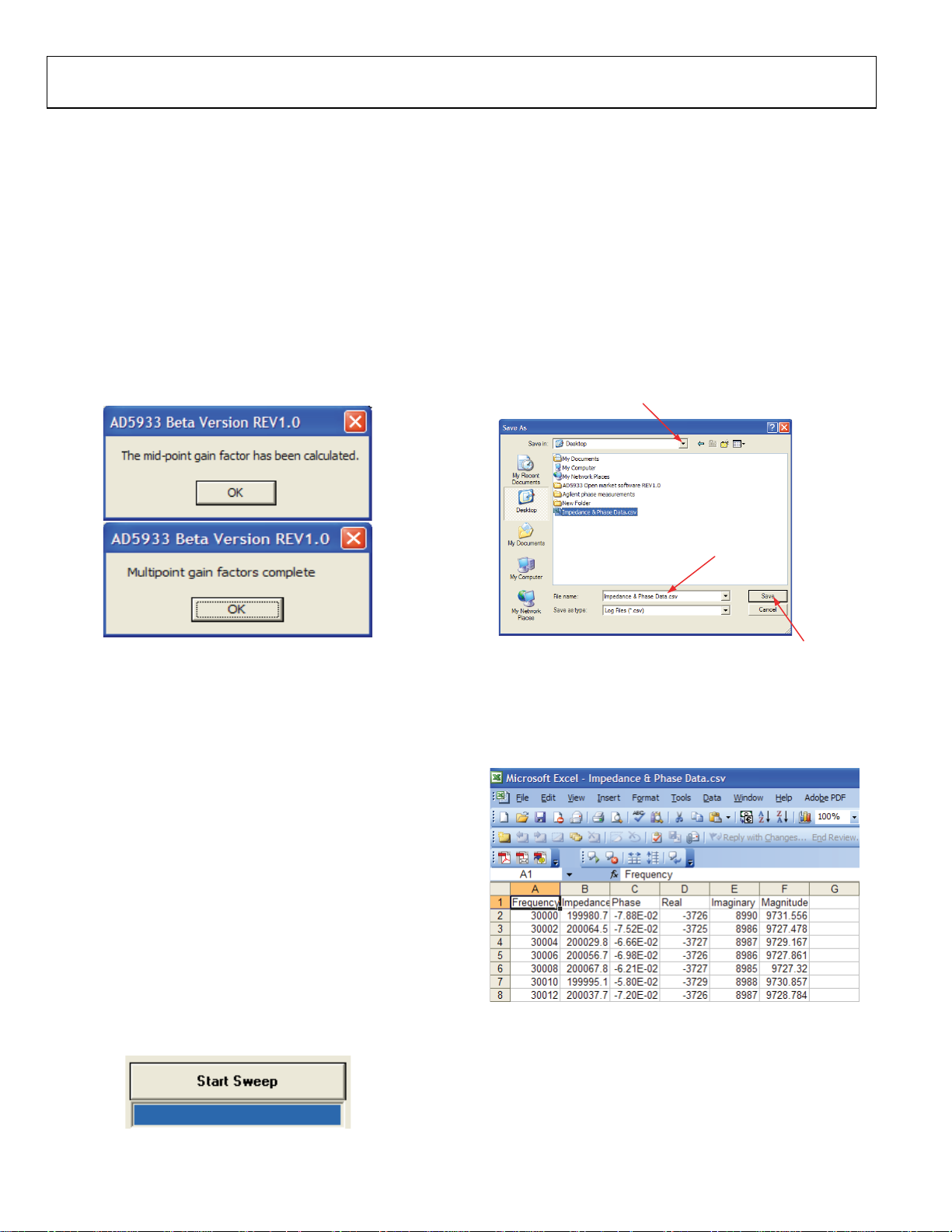
• To automatically calculate the gain factor(s) for the
subsequent sweep, click Calculate Gain Factor. The
evaluation software evaluates either a single midpoint
frequency gain factor or multipoint frequency gain factors,
that is, a gain factor for each point in the programmed sweep
(see 4 in Figure 12). The midpoint gain factor is determined
at the midpoint of the programmed sweep, and the multipoint
gain factors are determined at each point in the programmed
frequency sweep.
When either the midpoint gain factor or the multipoint gain
factors are calculated, a message appears on the evaluation
board software front panel, as shown in Figure 13. The gain
factor(s) returned to the evaluation software are subsequently
used for the sweep across the impedance under test.
• Click Measure in the Internal Temperature section of the
evaluation board software front panel to take a reading
from the on-board temperature sensor. This returns the
13-bit temperature of the device. See AD5933 data sheet
for more information on the temperature sensor.
• Click Download Impedance Data to download the frequency
sweep data (that is, frequency, impedance phase, real,
imaginary, and magnitude data) from the DFT of the sweep
(see 5 in Figure 12). The common dialog front panel is
presented as shown in Figure 15. Choose a file name in a
directory of choice and click Save (see Figure 15). This
saves the sweep data to a comma separated variable file
(.CSV) located in the chosen directory.
1. CHOOSE
DIRECTORY
2. CHOOSE
FILE NAME
10441-014
Figure 13. Confirmation of a Midpoint Calculation or
a Multipoint Gain Factors Calculation
After the system interface software calculates the gain factor(s)
for the programmed sweep parameters, the results are shown
in the Calculated Gain Factor box.
Note that should any of the system gain settings (for example,
change in output excitation range or PGA gain) change after
the system is calibrated (that is, gain factor(s) are calculated),
it is necessary to recalculate the gain factor(s) to subsequently
measure accurate impedance results. The gain factor(s)
calculated in the software are not programmed into the
AD5933 RAM and are only valid when the evaluation
software program is open and running. The gain factor(s)
are not retained in the evaluation software when the software
program is closed.
• Click Start Sweep (see 5 in Figure 12) to begin the sweep.
Once the evaluation software completes the sweep, it
automatically returns both a plot of the impedance vs.
frequency and phase vs. frequency for the impedance
under test (see Figure 12).The progress of the sweep is
outlined with a progress bar, as shown in Figure 14.
10441-015
Figure 14. Sweep Progress Bar (Blue)
3. SAVE THE FILE
Figure 15. Saving the Sweep Data
The contents of this file can be accessed by using Notepad
or Microsoft Excel to plot the data. Each file contains a single
column of data. The format of the downloaded data is shown
in Figure 16.
Figure 16. Opening the Sweep Data in Excel
10441-016
10441-017
Rev. 0 | Page 8 of 28
Page 9
Evaluation Board User Guide UG-364
Each data entry corresponds to a single measurement
(frequency) point; therefore, if the value for the number of
increments is programmed as 511 point, the array contains
a single column of data with 512 data points, starting at the
start frequency and ending at stop frequency value, which
is determined by
Start Frequency + (Number of Increments × Delta
Frequency)
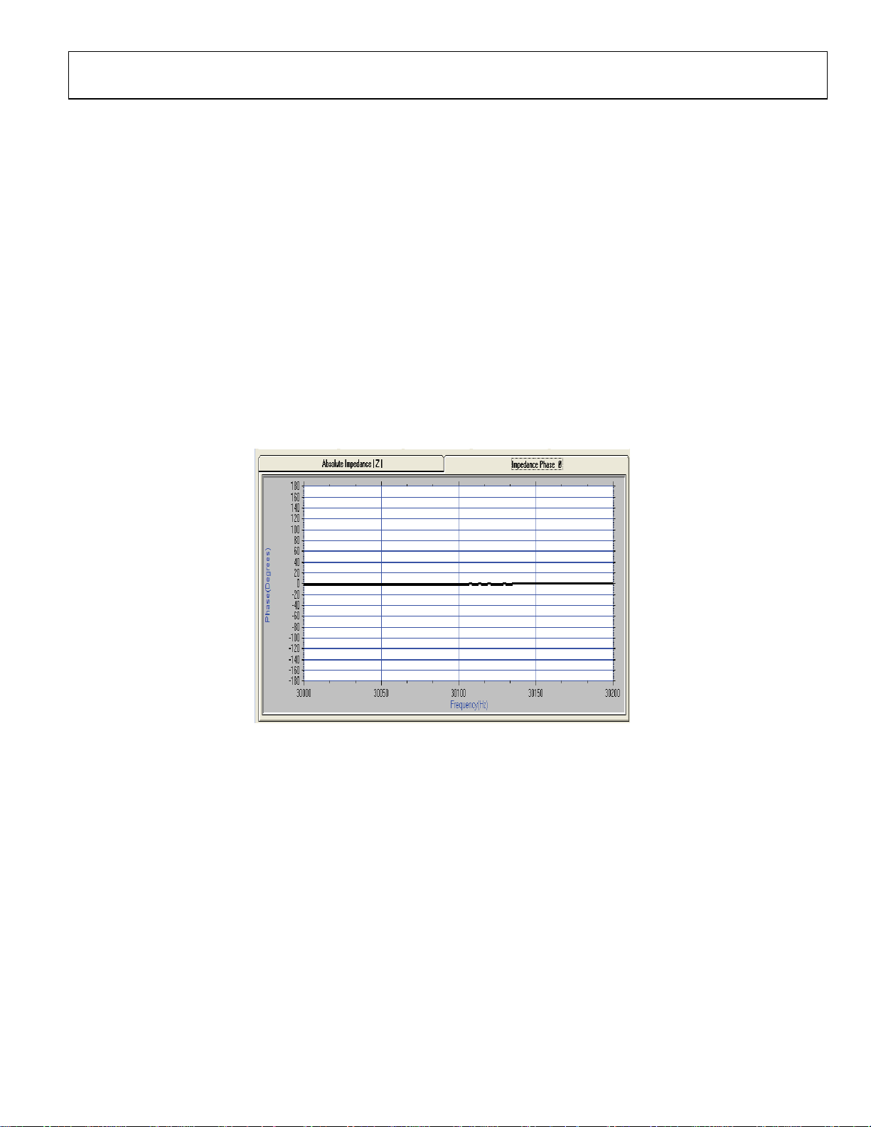
The impedance profile and phase profile vs. frequency appears
in the evaluation software front panel after the sweep has
completed. Click the individual tabs to switch between
Absolute Impedance |Z| and Impedance Phase Ø. Click
Absolute Impedance |Z| to show how the impedance under
analysis (Z
) varies across the programmed frequency
UNKNOWN
range. To view how the phase across the network under
analysis varies, click Impedance Phase Ø, as shown
in Figure 17.
Note that the phase measured by the AD5933 takes into
account the phase introduced through the entire signal path,
that is, the phase introduced through the output amplifiers,
receive current-to-voltage (I-V) amplifier, and the low-pass
filter, along with the phase through the impedance (Z
analysis connected between VOUT and VIN (Pin 6 and Pin 5
of the AD5933). Calibrate out the phase of the system using
a resistor before any subsequent impedance (Z
) phase
Ø
measurement is calculated. Calibrate with a resistor in the
evaluation software to calibrate the system phase correctly
(refer to the Impedance Measurement Tips section for
further details).
) under
Ø
10441-018
Figure 17. The Phase Tab on the A D5933 Evaluation Software Front Panel, Phase of 200 kΩ Resistor (0°) Displayed
Rev. 0 | Page 9 of 28
Page 10

UG-364 Evaluation Board User Guide
TWO INSTALLATION FREQUENTLY ASKED QUESTIONS
Q: How can I confirm that the hardware was correctly installed
on the PC?
A: To confirm the hardware was correctly installed on the PC,
use the following steps:
1. Right-click My Computer and left-click Properties.
2. Go to the Hardware tab, and click Device Manager (see
Figure 18).
3. Scroll to Universal Serial Bus controllers and expand the
root directory (see Figure 19). When the AD5933 hardware is
correctly installed, each time the USB cable connecting the
evaluation board to the computer is plugged in, the items
within the Universal Serial Bus controllers are refreshed.
Figure 19 shows what to expect when the AD5933 evaluation
board is correctly installed and when the evaluation board and
USB cable are connected correctly to the computer. The root
directory is subsequently refreshed when the USB cable is
unplugged from evaluation board, and the AD5933 evaluation
kit icon is removed from the main root.
Figure 18. System Properties
EXPAND ROOT
DIRECTORY
10441-019
Rev. 0 | Page 10 of 28
Figure 19. Correctly Installed Hardware
10441-020
Page 11

Evaluation Board User Guide UG-364
Q: During installation, when the board is plugged in for the first
time, the message shown in Figure 20 appears. When I click
Finish, the message shown in Figure 21 appears. What do I do
next?
10441-021
Figure 20. Error During the Hardware Installation
Figure 21. Found New Hardware Issue
A: If the evaluation software is installed correctly (install the
software correctly prior to plugging in the board for the first
time), this message simply indicates that the AD5933 device
drivers have not been installed to the correct registry and,
therefore, could not be correctly located by the install wizard.
To reinstall the device drivers, use the following steps:
1. Right-click My Computer, and left-click Properties.
2. Go to the Hardware tab, select Device Manager, and
expand Other devices (see Figure 22). The computer has
not recognized the USB device, that is, the AD5933
evaluation board.
3. Right-click USB Device and select Uninstall Driver.
4. Unplug the evaluation board and wait approximately
30 seconds before plugging it in again.
5. Proceed through the installation wizard a second time. The
expanded root directory shown in Figure 19 is a correct
installation. If the same error message is encountered the
second time, uninstall the device driver, uninstall the
software, and contact Analog Devices applications support
at www.analog.com for further instructions regarding valid
driver files.
1. EXPAND TH IS
DIRECTORY
Figure 22. USB Device Not Recognized
10441-022
Figure 23. Correctly Installed Hardware
2. RIGHT CLICK
ON THIS DE VICE
CORRECTLY INSTALLED
HARDWARE
10441-023
10441-024
Rev. 0 | Page 11 of 28
Page 12

UG-364 Evaluation Board User Guide
SOURCE CODE FOR IMPEDANCE SWEEP
PROGRAM F REQUENCY SWEEP PARAMETERS
INTO RELEVANT REGI STERS
(1) START FREQUENCY REG ISTER
(2) NUMBER OF INCREMENTS REG ISTER
(3) FREQUENCY INCREMENT REGISTER
PLACE THE AD5933 IN TO STANDBY MODE.
RESET: BY ISSUING A RESET COMMAND TO
THE CONTROL REGISTER, THE DEVICE IS
PLACED IN S TANDBY MODE.
PROGRAM THE INITIALIZE WITH START
FREQUENC Y COMMAND TO THE CO NTROL
AFTER A SUFFICI ENT AMOUNT OF SETTLING
TIME HAS ELAPSED, PROGRAM THE START
FREQUENC Y SWEEP COMMAND IN T HE
POLL THE STATUS REGISTER TO CHECK IF
THE DFT CONVERSION IS COMPLETE.
REGISTER.
CONTROL REG ISTER.
N
Y
READ VALUES FROM THE REAL AND
IMAGINARY DATA REGISTER.
POLL THE STATUS REGISTER TO CHECK IF
FREQUENC Y SWEEP IS COMPL ETE.
PROGRAM T HE AD5933
INTO POWER-DOWN MODE.
Figure 24. Sweep Flow Outline
This section outlines the evaluation board code structure required
to set up the AD5933 frequency sweep. The sweep flow outline is
shown in Figure 24. Each section of the flow diagram is explained
with the help of the visual basic code extracts. The firmware
code (c code), which is downloaded to the USB microcontroller
connected to the AD5933, implements the low level I
2
C signal
control (that is, read and write vendor request).
The code extract, which is shown in the Evaluation Board
Source Code Extract section, shows how to program a single
frequency sweep starting at 30 kHz, with a frequency step of
10 Hz and with 150 points in the sweep. The code assumes
that a 16 MHz clock signal is connected to Pin 8 (MCLK) of
PROGRAM T HE INCREMENT FREQUE NCY OR
THE REPEAT FREQUENCY COMMAND TO THE
Y
N
Y
CONTROL REG ISTER.
the AD5933. The impedance range under test is from 90 kΩ
to 110 kΩ. The gain factor is calculated at the midpoint of the
frequency sweep, that is, 30.750 kHz. The calibration is carried
out with a 100 kΩ resistor connected between VOUT and VIN.
The feedback resistor = 100 kΩ.
The first step in Figure 24 is to program the three sweep
parameters necessary to define the frequency sweep (that is,
the start frequency, number of increments, and frequency
increments). Refer to the AD5933 data sheet for more details.
10441-025
Rev. 0 | Page 12 of 28
Page 13

Evaluation Board User Guide UG-364
EVALUATION BOARD SOURCE CODE EXTRACT
‘------------------------------------------------------------------------------------------------------‘Code developed using visual basic® 6.
‘Datatype range
‘Byte 0-255
‘Double -1.797e308 to – 4.94e-324 and 4.94e-324 to 1.7976e308
‘Integer -32,768 to 32767
‘Long -2,147,483,648 to 2,147,483,647
‘Variant‘...when storing numbers same range as double. When storing strings same range as string.
‘-------------------------------------- Variable Declarations ----------------------------------------Dim ReadbackStatusRegister As Long 'stores the contents of the status register.
Dim RealData As Double 'used to store the 16 bit 2s complement real data.
Dim RealDataUpper As Long 'used to store the upper byte of the real data.
Dim RealDataLower As Long 'used to store the lower byte of the real data.
Dim ImagineryData As Double 'used to store the 16 bit 2s complement real data.
Dim ImagineryDataLower As Long 'used to store the upper byte of the imaginary data.
Dim ImagineryDataUpper As Long 'used to store the lower byte of the imaginary data.
Dim Magnitude As Double 'used to store the sqrt (real^2+imaginary^2).
Dim Impedance As Double 'used to store the calculated impedance.
Dim MaxMagnitude As Double 'used to store the max impedance for the y axis plot.
Dim MinMagnitude As Double 'used to store the min impedance for the y axis plot.
Dim sweep_phase As Double 'used to temporarily store the phase of each sweep point.
Dim Frequency As Double 'used to temporarily store the current sweep frequency.
Dim Increment As Long 'used as a temporary counter
Dim i As Integer 'used as a temporary counter in (max/min) mag,phase loop
Dim xy As Variant 'used in the stripx profile
Dim varray As Variant
Dim Gainfactor as double ‘either a single mid point calibration or an array of calibration points
Dim TempStartFrequency As Double
Dim StartFrequencybyte0 As Long
Dim StartFrequencybyte2 As Long
Dim StartFrequencybyte1A As Long
Dim StartFrequencybyte1B As Long
Dim DDSRefClockFrequency As Double
Dim NumberIncrementsbyte0 As Long
Dim NumberIncrementsbyte1 As Long
Dim FrequencyIncrementbyt0 As Long
Dim FrequencyIncrementbyt1 As Long
Dim FrequencyIncrementbyt2 As Long
Dim SettlingTimebyte0 As Long
Dim SettlingTimebyte1 As Long
‘-------------------------------------- I^2C read/write definitions----------------------------------------‘used in the main sweep routine to read and write to AD5933.This is the vendor request routines in the
firmware
Private Sub WritetToPart(RegisterAddress As Long, RegisterData As Long)
PortWrite &HD, RegisterAddress, RegisterData
‘parameters = device address register address register data
End Sub
Public Function PortWrite(DeviceAddress As Long, AddrPtr As Long, DataOut As Long) As Integer
PortWrite = VendorRequest(VRSMBus, DeviceAddress, CLng(256 * DataOut + AddrPtr), VRWRITE, 0, 0)
End Function
Public Function PortRead(DeviceAddress As Long, AddrPtr As Long) As Integer
PortRead = VendorRequest(VRSMBus, DeviceAddress, AddrPtr, VRREAD, 1, DataBuffer(0))
PortRead = DataBuffer(0)
End Function
‘------------------------------------- PHASE CONVERSION FUNCTION DEFINITION -------------------------------‘This function accepts the real and imaginary data(R, I) at each measurement sweep point and converts it to
a degree
‘-----------------------------------------------------------------------------------------------------------
Public Function phase_sweep (ByVal img As Double, ByVal real As Double) As Double
Dim theta As Double
Dim pi As Double
pi = 3.141592654
If ((real > 0) And (img > 0)) Then
theta = Atn(img / real) ' theta = arctan (imaginary part/real part)
phase2 = (theta * 180) / pi 'convert from radians to degrees
Rev. 0 | Page 13 of 28
Page 14

UG-364 Evaluation Board User Guide
ElseIf ((real > 0) And (img < 0)) Then
theta = Atn(img / real) '4th quadrant theta = minus angle
phase2 = ((theta * 180) / pi ) +360
ElseIf ((real < 0) And (img < 0)) Then
theta = -pi + Atn(img / real) '3rd quadrant theta img/real is positive
phase2 = (theta * 180) / pi
ElseIf ((real < 0) And (img > 0)) Then
theta = pi + Atn(img / real) '2nd quadrant img/real is neg
phase2 = (theta * 180) / pi
End If
End Function
‘-----------------------------------------------------------------------------------------------------------
Private Sub Sweep ()
’ the main sweep routine
‘This routine coordinates a frequency sweep using a mid point gain factor (see datasheet).
'The gain factor at the mid-point is determined from the real and imaginary contents returned at this mid
‘point frequency and the calibration impedance.
'The bits of the status register are polled to determine when valid data is available and when the sweep is
‘complete.
'----------------------------------------------------------------------------------------------------------IndexArray = 0 'initialize counter variable.
Increment = NumberIncrements + 1 'number of increments in the sweep.
Frequency = StartFrequency 'the sweep starts from here.
‘------------------------- PROGRAM 30K Hz to the START FREQUENCY register ---------------------------------
DDSRefClockFrequency = 16E6 ‘Assuming a 16M Hz clock connected to MCLK
StartFrequency = 30E3 ‘frequency sweep starts at 30K Hz
TempStartFrequency = (StartFrequency / (DDSRefClockFrequency / 4)) * 2^27 ‘dial up code for the DDS
TempStartFrequency = Int(TempStartFrequency) ‘30K Hz = 0F5C28 hex
StartFrequencybyte0 = 40 ‘40 DECIMAL = 28 HEX
StartFrequencybyte1 = 92 ‘92 DECIMAL = 5C HEX
StartFrequencybyte2 = 15 ’15 DECIMAL = 0F HEX
'Write in data to Start frequency register
WritetToPart &H84, StartFrequencybyte0 '84 hex lsb
WritetToPart &H83, StartFrequencybyte1 '83 hex
WritetToPart &H82, StartFrequencybyte2 '82 hex
‘--------------------------------- PROGRAM the NUMBER OF INCREMENTS register -----------------------------‘The sweep is going to have 150 points 150 DECIMAL = 96 hex
'Write in data to Number Increments register
WritetToPart &H89, 96 ‘lsb
WritetToPart &H88, 00 ‘msb
‘--------------------------------- PROGRAM the FREQUENCY INCREMENT register -----------------------------‘The sweep is going to have a frequency increment of 10Hz between successive points in the sweep
DDSRefClockFrequency = 16E6 ‘Assuming a 16M Hz clock connected to MCLK
FrequencyIncrements = 10 ‘frequency increment of 10Hz
TempStartFrequency = (FrequencyIncrements / (DDSRefClockFrequency / 4)) * 2^27 ‘dial up code for the DDS
TempStartFrequency = Int(TempStartFrequency) ’10 Hz = 335 decimal = 00014F hex
FrequencyIncrementbyt0 = 4F ‘335 decimal = 14f hex
FrequencyIncrementbyt1 = 01
FrequencyIncrementbyt2 = 00
'Write in data to frequency increment register
WritetToPart &H87, FrequencyIncrementbyt0 '87 hex lsb
WritetToPart &H86, FrequencyIncrementbyt1 '86 hex
WritetToPart &H85, FrequencyIncrementbyt2 '85 hex msb
‘--------------------------------- PROGRAM the SETTLING TIME CYCLES register -----------------------------‘The DDS is going to output 15 cycles of the output excitation voltage before the ADC will start sampling
‘the response signal. The settling time cycle multiplier is set to x1
Rev. 0 | Page 14 of 28
Page 15

Evaluation Board User Guide UG-364
SettlingTimebyte0 = 0F ‘15 cycles (decimal) = 0F hex
SettlingTimebyte1 = 00 ’00 = X1
WritetToPart &H8B, SettlingTimebyte0
WritetToPart &H8A, SettlingTimebyte1
‘-------------------------------------- PLACE AD5933 IN STANDBYMODE ----------------------------------------
‘Standby mode command = B0 hex
WritetToPart &H80, &HB0
'------------------------- Program the system clock and output excitation range and PGA setting----------‘Enable external Oscillator
WritetToControlRegister2 &H81, &H8
‘Set the output excitation range to be 2vp-p and the PGA setting to = x1
WritetToControlRegister2 &H80, &H1
‘----------------------------------------------------------------------------------------------------------‘------------- ------------ Initialize impedance under test with start frequency --------------------------'Initialize Sensor with Start Frequency
WritetToControlRegister &H80, &H10
msDelay 2 'this is a user determined delay dependent upon the network under analysis (2ms delay)
‘-------------------------------------- Start the frequency sweep -----------------------------------------'Start Frequency Sweep
WritetToControlRegister &H80, &H20
'Enter Frequency Sweep Loop
ReadbackStatusRegister = PortRead(&HD, &H8F)
ReadbackStatusRegister = ReadbackStatusRegister And &H4 ' mask off bit D2 (i.e. is the sweep complete)
Do While ((ReadbackStatusRegister <> 4) And (Increment <> 0))
'check to see if current sweep point complete
ReadbackStatusRegister = PortRead(&HD, &H8F)
ReadbackStatusRegister = ReadbackStatusRegister And &H2
'mask off bit D1 (valid real and imaginary data available)
‘------------------------------------------------------------------------ If (ReadbackStatusRegister = 2) Then
' this sweep point has returned valid data so we can proceed with sweep
Else
Do
‘if valid data has not been returned then we need to pole stat reg until such time as valid data
'has been returned
‘i.e. if point is not complete then Repeat sweep point and pole status reg until valid data
returned
WritetToControlRegister &H80, &H40 'repeat sweep point
Do
ReadbackStatusRegister = PortRead(&HD, &H8F)
ReadbackStatusRegister = ReadbackStatusRegister And &H2
' mask off bit D1- Wait until dft complete
Loop While (ReadbackStatusRegister <> 2)
Loop Until (ReadbackStatusRegister = 2)
End If
'-------------------------------------------------------------------------
RealDataUpper = PortRead(&HD, &H94)
RealDataLower = PortRead(&HD, &H95)
RealData = RealDataLower + (RealDataUpper * 256)
'The Real data is stored in a 16 bit 2's complement format.
'In order to use this data it must be converted from 2's complement to decimal format
If RealData <= &H7FFF Then ' h7fff 32767
' Positive
Else
' Negative
' RealData = RealData And &H7FFF
RealData = RealData - 65536
End If
ImagineryDataUpper = PortRead(&HD, &H96)
Rev. 0 | Page 15 of 28
Page 16

UG-364 Evaluation Board User Guide
ImagineryDataLower = PortRead(&HD, &H97)
ImagineryData = ImagineryDataLower + (ImagineryDataUpper * 256)
'The imaginary data is stored in a 16 bit 2's complement format.
'In order to use this data it must be converted from 2's complement to decimal format
If ImagineryData <= &H7FFF Then
' Positive Data.
Else
' Negative
' ImagineryData = ImagineryData And &H7FFF
ImagineryData = ImagineryData - 65536
End If
‘-----------------Calculate the Impedance and Phase of the data at this frequency sweep point ---------- Magnitude = ((RealData ^ 2) + (ImagineryData ^ 2)) ^ 0.5
'the next section calculates the phase of the dft real and imaginary components
‘phase_sweep calculates the phase of the sweep data.
sweep_phase = (phase_sweep(ImagineryData, RealData) - calibration_phase_mid_point)
GainFactor = xx ‘this is determined at calibration. See gain factor section and Datasheet.
Impedance = 1 / (Magnitude * GainFactor)
' Write Data to each global array.
MagnitudeArray(IndexArray) = Impedance
PhaseArray(IndexArray) = sweep_phase
ImagineryDataArray(IndexArray) = ImagineryData
code(IndexArray) = Magnitude
RealDataArray(IndexArray) = RealData
Increment = Increment - 1 ' increment was set to number of increments of sweep at the start
FrequencyPoints(IndexArray) = Frequency
Frequency = Frequency + FrequencyIncrements ' holds the current value of the sweep freq
IndexArray = IndexArray + 1
------------- Check to see if sweep complete ---------------------ReadbackStatusRegister = PortRead (&HD, &H8F)
ReadbackStatusRegister = ReadbackStatusRegister And &H4 ' mask off bit D2
'Increment to next frequency point Frequency
WritetToControlRegister &H80, &H30
Loop
‘--------------------- END OF SWEEP: Place device into POWERDOWN mode-----------------------------------'Enter Powerdown Mode,Set Bits D15,D13 in Control Register.
WritetToPart &H80, &HA0
END SUB
‘--------------------------------------------------------------------------------------------------------
‘The programmed sweep is now complete and the impedance and phase data is available to read in the two
‘arrays MagnitudeArray() = Impedance and PhaseArray() = phase.
sweepErrorMsg:
MsgBox "Error completing sweep check values"
End Sub
‘The programmed sweep is now complete and the impedance and phase data is available to read in the two
‘arrays MagnitudeArray() = Impedance and PhaseArray() = phase.
Rev. 0 | Page 16 of 28
Page 17

Evaluation Board User Guide UG-364
GAIN FACTOR CALCULATION
The code shown in the Evaluation Board Source Code Extract
section for the impedance sweep is based on a single point gain
factor calculation. This calculation is carried out once system
calibration is at the midpoint sweep frequency and with a
known impedance connected between VOUT and VIN. The
gain factor is calculated by exciting the calibration impedance with
a 2 V p-p sinusoid with a frequency of 30.750 kHz. The PGA
setting is ×1. The calibration is carried out with a 100 kΩ
resistor connected between VOUT and VIN. The feedback
resistor is 100 kΩ. The magnitude of the real and imaginary
component at the calibration frequency is given by the formula
22
IRMagnitude +=
where:
R is the real component.
I is the imaginary component of the calibration code.
Example Code for Temperature Measurement
Private Sub MeasureTemperature()
' The Digital temperature Result is stored over two registers as a 14 bit twos complement number.
' 92H <D15-D8> and 93H<D7 to D0>.
Dim TemperatureUpper As Long.
Dim TemperatureLower As Long
'Write xH90 to the control register to take t empera ture readi ng.
WritetToPart &H80, &H90
msDelay 5 'nominal delay
ReadbackStatusRegister = PortRead(&HD, &H8F)
ReadbackStatusRegister = ReadbackSta tusRegiste r And &H1
'if a valid temperature conversion i s complete , igno re this.
If ReadbackStatusRegister <> 1 Then
'loop to wait for temperatur e measurem ent to complete.
Do
ReadbackStatusRegister = PortRead (&HD, &H8F )
ReadbackStatusRegister = Readback StatusRegi ster A nd &H1
Loop Until (ReadbackStatusRegist er = 1)
Form1.Label10.Caption = "Cur rent Devic e Temp erature"
MsgBox "Device Temperature M easurement Compl ete"
End If
' The Digital temperature Result is stored over two registers as a 14 bit twos complement number.
' 92H <D15-D8> and 93H<D7 to D0>.
TemperatureUpper = PortRead(&HD, &H92)
TemperatureLower = PortRead(&HD, &H93)
Temperature = TemperatureLower + (Te mperatureU pper * 256)
If Temperature <= &H1FFF Then ' msb =0.
' Positive Temperature.
Label8.Caption = (Temperature / 32#)
Else
' Negative Temperature.
Rev. 0 | Page 17 of 28
The gain factor is then given by
⎞
1
⎟
⎟
⎠
=
MagnitudeMagnitude
⎟
⎜
⎟
⎜
k100
⎠
⎝
GainFactor
Admittance
⎛
=
⎜
⎝
Code
⎞
=
⎟
⎠
⎛
⎜
⎜
Impedance
⎝
⎞
⎛
1
Refer to the AD5933 data sheet for more details.
TEMPERATURE MEASUREMENT
Refer to the AD5933 data sheet for details on the temperature
sensor. The temperature sensor data is stored in a 14-bit twos
complement format. The conversion formula is given in the
AD5933 data sheet.
Page 18

UG-364 Evaluation Board User Guide
r
g
V
Label8.Caption = (Temperature - 16384) / 32#
End If
're-assign variables used.
TemperatureUpper = 0
TemperatureLower = 0
Temperature = 0
End Sub
IMPEDANCE MEASUREMENT TIPS
This section outlines some of the workarounds for using the
AD5933 to measure the impedance profiles under certain
conditions.
Calibrating the AD5933
When calculating the calibration term (that is, gain factor, see
the AD5933 data sheet for further details), it is important that
the receive stage operates in its linear region. This requires careful
selection of the system gain settings. The system gain settings
include the following:
• Output excitation voltage range
• Current-to-voltage gain setting resistor
• PGA gain
The gain through the system shown in Figure 25 is given by
Resisto
Settin
Output Excitation Voltage Range ×
PGA Gain
CURRENT-TO-VOLTAGE
GAIN SETTING RESISTOR
RFB
Z
OUT
UNKNOWN
VIN
VDD
Figure 25. AD5933 System Voltage Gain
For example, assume the following system calibration settings:
• VDD = 3.3 V
• Gain setting resistor = 200 kΩ
• Z
UNKNOWN
= 200 kΩ
• PGA setting = ×1
• Range 1 = 2 V p-p
The peak-to-peak voltage presented to the ADC input is 2 V p-p.
However, if a programmable gain amplifier setting gain of ×5 is
chosen, the voltage saturates the ADC, and the calculated
calibration term (that is, the gain factor) is inaccurate due to the
saturation of the ADC.
Gain
PGA
(×1 OR ×5)
Z
UNKNOWN
LPF
×
ADC
Rev. 0 | Page 18 of 28
10441-026
Calculate the gain factor when the largest response signal is
presented to the ADC while ensuring that the signal is always
maintained within the linear range of the ADC over the impedance
range of interest (the reference range of the ADC is the AVDD
supply).
Configure the system gain settings (see Figure 25), that is, the
output excitation voltage range (Range 1, Range 2, Range 3, or
Range 4), the I-V amplifier gain setting resistor based on the
unknown impedance range of interest, and the programmable
gain amplifier setting (either ×1 or ×5) that proceeds the ADC.
Choose a calibration impedance that is midvalue between the limits
of the unknown impedance; therefore, the user must know the
impedance limits to correctly calibrate the system. Then choose an
equal value I-V gain setting resistor to the calibration impedance.
This results in a unity gain condition about the receive side of
the I-V amplifier.
For example, assume the following:
• Unknown test impedance limits are 180 kΩ ≤ Z
UNKNOWN
≤
220 kΩ
• Frequency range of interest is 30 kHz to 32 kHz
The following are the system calibration gain settings:
• VDD = 3.3 V
• Gain setting resistor (R
• Z
CALIBRATION
= 200 kΩ
) = 200 kΩ
FB
• PGA setting = ×1
• Calibration frequency = 31 kHz (midpoint frequency)
The gain factor calculated at the midpoint frequency of 31 kHz
can be used to calculate any impedance in the 180 k to 220
region. Impedance results degrade if the unknown impedance span
is large or if the frequency sweep is large. If any of the calibration
system gain settings change, recalibrate the AD5933 and recalculate
the gain factor (see AD5933 data sheet for further details).
Page 19

Evaluation Board User Guide UG-364
Measuring Lower Excitation Frequencies
The AD5933 has a flexible internal DDS core and a digital-toanalog converter (DAC) that together generate the excitation
signal used to measure the impedance (Z
UNKNOWN
). The DDS core
has a 27-bit phase accumulator that allows subhertz (0.1 Hz)
frequency resolution. The output of the phase accumulator is
connected to the input of a read-only memory (ROM).The digital
output of the phase accumulator is used to address individual
memory locations in the ROM. The digital contents of the ROM
represent amplitude samples of a single cycle of a sinusoidal
excitation waveform. The contents of each address within the
ROM look-up table are in turn passed to the input of a DAC that
produces the analog excitation waveform made available at the
VOUT pin. The DDS core (that is, the phase accumulator and the
ROM look-up) and the DAC are all referenced from a single system
clock. The function of the phase accumulator is simply to act as
a system clock divider.
The system clock for the AD5933 DDS engine can be provided
in one of two ways.
• The user can provide a highly accurate and stable clock
(crystal oscillator) at the external clock pin, MCLK (Pin 8).
• Alternatively, the AD5933 provides an internal clock oscillator
with a typical frequency of 16.776 MHz.
The user can select the preferred system clock by programming
Bit D3 in the control register (Address 0x81, see the AD5933
data sheet).
The internal ADC also uses the system clock to digitize the
response signal. The ADC requires 16 clock periods to perform
a single conversion. Therefore, with a maximum system clock
frequency of 16.776 MHz, the ADC can sample the response
signal with a frequency of 1.0485 MHz, that is, a throughput
rate of ≈ 1.04 MSPS. The ADC converts 1024 samples and passes
the digital results to the MAC core for processing. The AD5933
MAC core performs a 1024 point DFT to determine the peak
of the response signal at the ADC input. The DFT offers many
advantages over conventional peak detection mechanisms,
including excellent dc rejection, an averaging of errors, and
phase information.
The throughput rate of the AD5933 ADC scales with the system
clock, that is, lower ADC throughput rates, and therefore sampling
frequencies can be achieved by lowering the system clock.
The conventional DFT assumes a sequence of periodic input
data samples to determine the spectral content of the original
continuous signal. In the AD5933, these samples obviously come
from the 12-bit ADC for a user-defined range of signal frequencies.
The conventional DFT correlates the input signal against a series
of test phasor frequencies to determine the fundamental signal
frequency and its harmonics. The frequency of the test phasor is
at integer multiples of a fundamental frequency given by the
following formula:
Test Phasor Frequency = (f
/N)
S
where:
f
is the sampling frequency of the ADC.
S
N is the number of samples taken equals 1024.
The correlation is performed for each frequency integer
fundamental. If the resulting correlation of the test phasor
with the input sample set is nonzero, there is signal energy at
this frequency. If no energy is found in a bin, there can be no
energy at that test frequency.
The DFT implemented by the AD5933 is called a single point
DFT; this means that the analysis or correlation frequency in
the MAC core is always at the same frequency as the current
output excitation frequency. Therefore, when the system clock
for the AD5933 is 16.776 MHz, the sample rate of the ADC is
1.04 MHz. The DSP core requires 1024 samples to perform
the single point DFT. Therefore, the resolution of the DFT is
1.04 MHz/1024 points ≈ 1 kHz. This calculation is based on
a system clock frequency of 16 MHz being applied at MCLK. If
the AD5933 tries to examine excitation frequencies below ≈ 1 kHz,
the errors introduced by the spectral leakage become significant
and result in erroneous impedance readings.
If the input signal does not have an exact integer number of cycles
over the 1024-point sample interval, as shown in Figure 26, there
will not be a smooth transition from the end of one period to
the next, as shown in Figure 27. The leakage is a result of the
discontinuities introduced by the DFT assuming a periodic
input signal like that shown in Figure 27.
SAMPLES SPAN ENTIRE EXCITATION PERIOD
SAMPLE
WINDOW
Figure 26. Sample Set Spanning the Entire Excitation Period
SAMPLES DO NOT SPAN ENTIRE EXCITATION PERIOD
DFT ASSUMES A PERIODIC
SAMPLE SET
10441-027
Rev. 0 | Page 19 of 28
DFT ASSUMES A PERIODIC
SAMPLE SET
Figure 27. Sample Set Not Spanning the Entire Excitation Period
10441-028
Page 20

UG-364 Evaluation Board User Guide
For the AD5933 to analyze the impedance (Z
UNKNOWN
) at
frequencies lower than ≈ 1 kHz, it is necessary to scale the system
clock such that the sample rate of the ADC is lowered and cause
the 1024 samples required for the single point DFT to cover an
integer number of periods of the current excitation frequency.
To analyze frequencies between the 1 kHz to 10 kHz range using
the AD5933 and a 16 MHz crystal, scale the system clock by
using an external clock divider. This reduces the sampling
frequency of the ADC to a value less than 1 MHz (f
SAMPLING
=
MCLK/16); however, the 1024 sample set now covers the
response signal under analysis. When scaling the system clock,
the maximum bandwidth of the sweep must be reduced.
To help analyze lower clock frequencies, scale the system clock
connected to the AD5933. This scaling establishes a lower
impedance limit (see Tabl e 2 ); however, the upper excitation
frequency is now limited.
Table 2. Experimental Lower Frequency Limits vs. MCLK
AD5933 Lower Frequency1
Clock Frequency Applied
to MCLK Pin
2
100 kHz to 5 kHz 16 MHz
5 kHz to 1 kHz 4 MHz
5 kHz to 300 Hz 2 MHz
300 Hz to 200 Hz 1 MHz
200 Hz to 100 Hz 250 kHz
100 Hz to 30 Hz 100 kHz
30 Hz to 20 Hz 50 kHz
20 Hz to 10 Hz 25 kHz
1
Lower frequency sweep limit established by applying the divided clock
signal to the MCLK pin of the AD5933 and by calibrating and remeasuring a
nominal impedance Z
linear sweep from the programmed start frequency (I-V gain resistor setting =
Z
, for example, 200 kΩ, PGA = X1. ΔFrequency = 5 Hz, and number
CALIBRATION
of points = 100). The lower frequency limit is established as the frequency at
which the DFT and, therefore, the impedance vs. the frequency results begin
to degrade and deviate from the expected value of the measured impedance
, for example, 200 kΩ.
Z
CALIBRATION
2
TTL clock levels applied to MCLK pin, VIH = 2 V, and VIL = 0.8 V.
, for example, a 200 kΩ resistor over a 500 Hz
CALIBRATION
As an example, if a scaled clock frequency of 4 MHz must be
applied to the external clock pin of the AD5933 to correctly
analyze a 3 kHz signal that has already been established. The
applied system clock (external or internal oscillator) is divided
by a factor of 4 before being routed as the reference clock to the
DDS. The system clock is directly connected to the ADC without
any divide so that the ADC sampling clock is running at 4 times
the speed of the DDS core. Therefore, with a system clock of 4
MHz, the DDS reference clock is now 1/4 × 4 MHz = 1 MHz,
and the ADC clock is 4 MHz. The AD5933 DDS has a 27-bit
phase accumulator; however, the top three most significant bits
(MSBs) are internally connected to logic zero. Therefore, with
the top three MSBs set to zero, the maximum DDS output
frequency is now reduced by a further factor of ⅛th. Therefore, the
maximum output frequency is now 1/32 × 1 MHz = 31.25 kHz.
Rev. 0 | Page 20 of 28
It is possible to accurately measure the 3 kHz signal using a lower
system clock of 4 MHz; however, the two main trade-offs are
that it takes the AD5933 longer to return the impedance results
due to the slower ADC conversion clock speed and that the
upper excitation limit is now restricted to 31.25 kHz.
Measuring Higher Excitation Frequencies
The AD5933 is specified to a typical system accuracy of 0.5%
(assuming the AD5933 system is calibrated correctly for the
impedance range under test) within the frequency range of 1 kHz
to 100 kHz. The lower frequency limit is determined by the value
of the system clock frequency connected to the external clock pin
(MCLK) of the AD5933. The lower limit can be reduced by scaling
the system clock (see the Measuring Lower Excitation Frequencies
section). The upper frequency limit of the system is due to the
finite bandwidth of the internal amplifiers coupled with the
effects of the low-pass filter pole locations (for example, 200 kHz
and 300 kHz), which are used to roll-off any noise signals from
corrupting the DFT output on the receive side of the AD5933.
Therefore, the AD5933 has a finite frequency response similar
to that shown in Figure 28.
20
0
–20
SYSTEM GAIN (dB)
–40
–60
100 1k 10k 100k 1M
Figure 28. Typical AD5933 System Bandwidth
SYSTEM BANDWIDTH (Hz)
10441-031
Using the AD5933 to analyze frequencies past 100 kHz introduces
errors in impedance profile if the sweep span is large, due to the
effect of the increased roll-off in the finite frequency response
of the system past 100 kHz. However, if the user is sweeping in
frequency above 100 kHz, it is important to ensure that the sweep
range is as small as possible, for example, 120 kHz to 122 kHz. The
impedance error from the calibration frequency is approximately
linear over a small frequency range. The user can remove the linear
error introduced by carrying out an endpoint/multipoint
calibration (see the Two Point Calibration section of the AD5933
data sheet for additional details on endpoint calibration).
Page 21

Evaluation Board User Guide UG-364
∇
∇
Measuring the Phase Across an Impedance
The AD5933 returns a complex output code made up of a separate
real and imaginary component. The real component is stored at
Register 0x94 and Register 0x95, and an imaginary component
is stored at Register 0x96 and Register 0x97 after each sweep
measurement. These correspond to the real and imaginary
components of the DFT and not the resistive and reactive
components of the impedance under test.
For example, it is a common misconception that when analyzing a
series RC circuit that the real value stored in Register 0x94 and
Register 0x95 and the imaginary value stored at Register 0x96
and Register 0x97 corresponds to the resistance and capacitive
reactance, respectfully. However, this is incorrect; the magnitude of
the impedance (|Z|) can be calculated by calculating the magnitude
of the real and imaginary components of the DFT given by
22
IRMagnitude +=
After each measurement, multiply it by the calibration term
(see gain factor calculation in AD5933 data sheet) and invert
the product. The magnitude of the impedance is therefore given by
Impedance×=
1
Magnitude FactorGain
where the Gain Factor is given by
⎛
⎜
⎜
Admittance
FactorGain
⎛
=
⎜
Code
⎝
⎞
=
⎟
⎠
Impedance
⎝
Magnitude
⎞
1
⎟
⎟
⎠
Before any valid measurement can take place, the AD5933 system
must be calibrated for a know impedance range to determine
the gain factor. Therefore, the impedance limits of the complex
impedance (Z
) for the sweep frequency range of interest
UNKNOWN
must be known. Place known impedance between the input/output
of the AD5933 and measure the resulting magnitude of the code
to determine what the gain factor is. The AD5933 system gain
settings must be chosen to place the excitation signal in the
linear region of the on-board ADC (refer to the AD5933 data
sheet for further details).
Because the AD5933 returns a complex output code made up of a
real and an imaginary component, the phase of the response
signal through the AD5933 signal path can be calculated. The
−1
phase is given by Phase (rads) = Tan
(I/R).
The phase measured by the previous formula accounts for the
phase shift introduced to the DDS output signal as it passes
through the internal amplifiers on the transmit and receive side
of the AD5933 along with the low-pass filter and the impedance
connected between the VOUT and VIN pins of the AD5933.
The AD5933 parameters of interest are the magnitude of the
impedance (|Z
|) and the impedance phase (ZØ). The
UNKNOWN
measurement of ZØ is a two-step process. The first step
involves calculating the AD5933 system phase. The AD5933
system phase can be calculated by placing a resistor across the
VOUT and VIN pins of the AD5933 and calculating the phase
(using the previous formula) after each measurement point in
the sweep. By placing a resistor across the VOUT and VIN pins,
there is no additional phase lead or lag introduced to the AD5933
signal path, and the resulting phase is due entirely to the internal
poles of the AD5933, that is, the system phase.
Once the system phase has been calibrated using a resistor, the
phase of any unknown impedance can be calculated by inserting
the unknown impedance between the VIN and VOUT terminals
of the AD5933 and by recalculating the new phase (including the
phase due to the impedance) using the previous formula. The
phase of the unknown impedance (ZØ) is given by
ZØ = (Φunknown − ) system∇
where:
system
is the phase of the system with a calibration resistor
connected between VIN and VOUT.
unknown is the phase of the system with the unknown
Φ
impedance connected between VIN and VOUT.
ZØ is the phase due to the impedance, that is, the impedance
phase.
Note that it is possible both to calculate the gain factor and to
calibrate the system phase using the same real and imaginary
component values when a resistor is connected between the
VOUT and VIN pins of the AD5933.
For example, measuring the impedance phase (ZØ) of a
capacitor.
The excitation signal current leads the excitation signal voltage
across a capacitor by −90°; therefore, before any measurement
is taken, expect to see an approximate −90° phase difference
between the system phase responses measured with a resistor
and the system phase responses measured with capacitive
impedance.
As previously outlined, to determine the phase angle of capacitive
system
impedance (ZØ), the system phase response (
) must be
determined and subtracted from the phase calculated with the
capacitor connected between VOUT and VIN (Φ
unknown).
Rev. 0 | Page 21 of 28
Page 22

UG-364 Evaluation Board User Guide
–
Figure 29 shows the AD5933 system phase response calculated
using a 220 k calibration resistor (R
= 220 k, PGA = ×1)
FB
and the repeated phase measurement with a 10 pF capacitive
impedance.
200
180
160
140
120
100
80
PHASE (Degrees)
60
40
20
0
0 15k 30k 45k 60k 75k 90k 105k 120k
220kΩ RESISTOR
10pF CAPACIT OR
FREQUENCY (Hz)
10441-032
Figure 29. System Phase Response vs. Capacitive Phase
The phase difference (that is, ZØ) between the phase response
of a capacitor and the system phase response using a resistor is
the impedance phase of the capacitor (ZØ) and is shown in
Figure 30.
100
–90
–80
–70
–60
–50
–40
PHASE (Degrees)
–30
–20
–10
0
0 15k 30k 45k 60k 75k 90k 105k 120k
FREQUENCY (Hz)
10441-033
Figure 30. Phase Response of a Capacitor
Note that the phase formula used to plot Figure 29 uses the
arctangent function that returns a phase angle in radians and,
therefore, it is necessary to convert from radians to degrees.
In addition, take care when using the arctangent formula when
using the real and imaginary values to interpret the phase at
each measurement point. The arctangent function returns the
correct standard phase angle only when the sign of the real and
imaginary values are positive, that is, when the coordinates lie in
the first quadrant. The standard angle is taken counter clockwise
from the positive real x-axis. If the sign of the real component is
positive and the sign of the imaginary component is negative, that
is, the data lies in the second quadrant, the arctangent formula
returns a negative angle, and it is necessary to add a further 180°
to calculate the correct standard angle. Likewise, when the real
and imaginary components are both negative, that is, when the
coordinates lie in the third quadrant, the arctangent formula
returns a positive angle, and it is necessary to add 180° to the
angle to return the correct standard phase. Finally, when the
real component is positive and the imaginary component is
negative, that is, the data lies in the fourth quadrant, the arctangent
formula returns a negative angle, and it is necessary to add 360° to
the angle to calculate the correct phase angle.
Therefore, the correct standard phase angle is dependent on the
sign of the real and imaginary component and is summarized in
Tabl e 3 .
Table 3. Phase Angle
Real Imaginary Quadrant Phase Angle (Degrees)
Positive Positive First
Positive Negative Second
Negative Negative Third
Positive Negative Fourth
180
−
1
⎛
⎜
⎝
⎛
⎜
⎝
⎛
⎜
⎝
×
)/(Tan
RI
π
180
−
1
−
1
−
1
⎞
)/(Tan180
RI
×+
⎟
π
⎠
180
⎞
)/(Tan180
RI
×+
⎟
π
⎠
180
⎞
)/(Tan360
RI
×+
⎟
π
⎠
Once the magnitude of the impedance (|Z|) and the impedance
phase angle (ZØ, in radians) are correctly calculated, it is possible
to determine the magnitude of the real (resistive) and imaginary
(reactive) components of the impedance (Z
UNKNOWN
) by the vector
projection of the impedance magnitude onto the real and
imaginary impedance axis using the following formulas:
The real component is given by
Z
| = |Z| × cos(ZØ)
|
REAL
The imaginary component is given by
Z
| = |Z| × sin(ZØ)
|
IMAG
Rev. 0 | Page 22 of 28
Page 23

Evaluation Board User Guide UG-364
EVALUATION BOARD SCHEMATICS AND ARTWORK
10441-034
Figure 31. EVAL-AD5933EBZ USB Schematic
Rev. 0 | Page 23 of 28
Page 24

UG-364 Evaluation Board User Guide
10441-035
Figure 32. EVAL-AD5933EBZ Schematic
Rev. 0 | Page 24 of 28
Page 25

Evaluation Board User Guide UG-364
10441-036
Figure 33. Linear Regulator on the EVAL-AD5933EB Evaluation Board
Rev. 0 | Page 25 of 28
Page 26

UG-364 Evaluation Board User Guide
ORDERING INFORMATION
BILL OF MATERIALS
Table 4.
Name Part Description Manufacturer Part Number
C1 to C31 Capacitor, MR04, place holder Not applicable Not applicable
Z1
C5 10 μF tantalum capacitor, 10 V AVX Corporation TAJB106K016R
C7 47 nF capacitor, 50 V, through hole, 10%, R1/8 W Multicomp MCRR50473X7RK0050
C9, C11, C22, C25, C31, C32, C25 10 μF ceramic capacitor, X5R, 0805 Yageo Corporation CC0805KKX5R6BB106
C14 2.2 μF ceramic capacitor, 6.3 V, X5R, 0603, SMD Yageo Corporation CC0603KRX5R5BB225
C6, C8, C10, C12, C13, C15 to C21,
C23, C24, C26, C27, C30, C33,
C34, C36
C28, C29 22 pF ceramic capacitor, 50 V, 5%, 0603, NPO, SMD Yageo Corporation CC0603JRNPO9BN220
CLK1 SMB socket
D4 Green LED, 0805 Avago Technologies HSMG-C170
GL1 Copper short ground link Not applicable Not applicable
J1 USB Mini-B connector Molex 56579-0576
J2 2-pin terminal block (5 mm pitch), CON\POWER Camden Electronics CTB5000/2
LK1 to LK6 Jumper block, 2 pins, 0.1" spacing, SIP-2P Harwin M20-9990246
R1, R2, R7 to R8 49.9 kΩ, SMD resistor, 1%, 0603 Multicomp MC 0.063W 0603 1% 49K9
CAL1 Place holder, insert 2-wire wrap pins, R1/8 W Analog Devices issue 73017015
R4 20 kΩ, SMD resistor (0.1%), 0603 Panasonic ERA3AEB203V
R5 20 kΩ, SMD resistor (0.1%), 0603 Multicomp MC 0.063W 0603 1% 20K
R61 Through hole resistor, 1/8 W Not applicable Not applicable
R10 1 kΩ, 0805, SMD resistor Multicomp MC 0.1W 0805 1% 1K
R11, R12 100 kΩ, 1%, 0603, SMD resistor Multicomp MC 0.063W 0603 1% 100K
R13 0 Ω, 1%, 0603, SMD resistor Multicomp MC 0.063W 0603 0R
R14 10 kΩ, 1%, 0603, SMD resistor Multicomp MC 0.063W 0603 1% 10K
R15, R16 2.2 kΩ, 1%, 0603 SMD resistor Multicomp MC 0.063W 0603 1% 2K2
T1 to T8 Black test point Vero Technologies 20-2137
U1
U2
U3 USB microcontroller, LFCSP-56 Cypress Semiconductor CY7C68013-56LFC
U4 I2C serial EEPROM, 64k, 2.5 V, 8-SOIC Microchip Technologies 24LC64-I/SN
U5, U6
Y1 24 MHz SMD crystal, XTAL-CM309S AEL Crystals X24M000000S244
Y2 3.3 V, 16 MHz clock oscillator AEL Crystals AEL4303
1
Do not install.
Capacitor, MR04, place holder, insert 2-wire
wrap pins
0.1 μF ceramic capacitor, 50 V, X7R, 10%, 0603, SMD AVX Corporation 06035C104KAT2A
Precision, low noise, CMOS, rail-to-rail, input/output
operational amplifiers
1 MSPS, 12-bit impedance converter network
analyzer
High accuracy anyCAP® 200 mA low dropout
linear regulator
Analog Devices issue 73017015
Tyco Electronics
Corporation
Analog Devices AD8606ARZ
Analog Devices AD5933BRSZ
Analog Devices ADP3303ARZ-3.3
1-1337482-0
Rev. 0 | Page 26 of 28
Page 27

Evaluation Board User Guide UG-364
RELATED LINKS
Resource Description
AD5933 1 MSPS, 12-bit impedance converter network analyzer
AD9834 20 mW power, 2.3 V to 5.5 V, 75 MHz complete DDS
ADF4001 200 MHz clock generator PLL
ADuC7020 Precision analog microcontroller, 12-bit analog I/O, ARM7TDMI® MCU
ADCMP601 Rail-to-rail, very fast, 2.5 V to 5.5 V, single-supply TTL/CMOS comparator in a 6-lead SC70 package
ADP3303 High accuracy anyCAP® 200 mA low dropout linear regulator
AD8606 Precision, low noise, CMOS, rail-to-rail, input/output operational amplifiers
Rev. 0 | Page 27 of 28
Page 28

UG-364 Evaluation Board User Guide
NOTES
ESD Caution
ESD (electrostatic discharge) sensitive device. Charged devices and circuit boards can discharge without detection. Although this product features patented or proprietary protection
circuitry, damage may occur on devices subjected to high energy ESD. Therefore, proper ESD precautions should be taken to avoid performance degradation or loss of functionality.
Legal Terms and Conditions
By using the evaluation board discussed herein (together with any tools, components documentation or support materials, the “Evaluation Board”), you are agreeing to be bound by the terms and conditions
set forth below (“Agreement”) unless you have purchased the Evaluation Board, in which case the Analog Devices Standard Terms and Conditions of Sale shall govern. Do not use the Evaluation Board until you
have read and agreed to the Agreement. Your use of the Evaluation Board shall signify your acceptance of the Agreement. This Agreement is made by and between you (“Customer”) and Analog Devices, Inc.
(“ADI”), with its principal place of business at One Technology Way, Norwood, MA 02062, USA. Subject to the terms and conditions of the Agreement, ADI hereby grants to Customer a free, limited, personal,
temporary, non-exclusive, non-sublicensable, non-transferable license to use the Evaluation Board FOR EVALUATION PURPOSES ONLY. Customer understands and agrees that the Evaluation Board is provided
for the sole and exclusive purpose referenced above, and agrees not to use the Evaluation Board for any other purpose. Furthermore, the license granted is expressly made subject to the following additional
limitations: Customer shall not (i) rent, lease, display, sell, transfer, assign, sublicense, or distribute the Evaluation Board; and (ii) permit any Third Party to access the Evaluation Board. As used herein, the term
“Third Party” includes any entity other than ADI, Customer, their employees, affiliates and in-house consultants. The Evaluation Board is NOT sold to Customer; all rights not expressly granted herein, including
ownership of the Evaluation Board, are reserved by ADI. CONFIDENTIALITY. This Agreement and the Evaluation Board shall all be considered the confidential and proprietary information of ADI. Customer may
not disclose or transfer any portion of the Evaluation Board to any other party for any reason. Upon discontinuation of use of the Evaluation Board or termination of this Agreement, Customer agrees to
promptly return the Evaluation Board to ADI. ADDITIONAL RESTRICTIONS. Customer may not disassemble, decompile or reverse engineer chips on the Evaluation Board. Customer shall inform ADI of any
occurred damages or any modifications or alterations it makes to the Evaluation Board, including but not limited to soldering or any other activity that affects the material content of the Evaluation Board.
Modifications to the Evaluation Board must comply with applicable law, including but not limited to the RoHS Directive. TERMINATION. ADI may terminate this Agreement at any time upon giving written notice
to Customer. Customer agrees to return to ADI the Evaluation Board at that time. LIMITATION OF LIABILITY. THE EVALUATION BOARD PROVIDED HEREUNDER IS PROVIDED “AS IS” AND ADI MAKES NO
WARRANTIES OR REPRESENTATIONS OF ANY KIND WITH RESPECT TO IT. ADI SPECIFICALLY DISCLAIMS ANY REPRESENTATIONS, ENDORSEMENTS, GUARANTEES, OR WARRANTIES, EXPRESS OR IMPLIED, RELATED
TO THE EVALUATION BOARD INCLUDING, BUT NOT LIMITED TO, THE IMPLIED WARRANTY OF MERCHANTABILITY, TITLE, FITNESS FOR A PARTICULAR PURPOSE OR NONINFRINGEMENT OF INTELLECTUAL
PROPERTY RIGHTS. IN NO EVENT WILL ADI AND ITS LICENSORS BE LIABLE FOR ANY INCIDENTAL, SPECIAL, INDIRECT, OR CONSEQUENTIAL DAMAGES RESULTING FROM CUSTOMER’S POSSESSION OR USE OF
THE EVALUATION BOARD, INCLUDING BUT NOT LIMITED TO LOST PROFITS, DELAY COSTS, LABOR COSTS OR LOSS OF GOODWILL. ADI’S TOTAL LIABILITY FROM ANY AND ALL CAUSES SHALL BE LIMITED TO THE
AMOUNT OF ONE HUNDRED US DOLLARS ($100.00). EXPORT. Customer agrees that it will not directly or indirectly export the Evaluation Board to another country, and that it will comply with all applicable
United States federal laws and regulations relating to exports. GOVERNING LAW. This Agreement shall be governed by and construed in accordance with the substantive laws of the Commonwealth of
Massachusetts (excluding conflict of law rules). Any legal action regarding this Agreement will be heard in the state or federal courts having jurisdiction in Suffolk County, Massachusetts, and Customer hereby
submits to the pers onal jurisdiction and venu e of such courts. The United Nations Conventi on on Contracts for the Internation al Sale of Goods shall not apply to this Agreement and is expressly disclaimed.
©2012 Analog Devices, Inc. All rights reserved. Trademarks and
registered trademarks are the property of their respective owners.
UG10441-0-2/12(0)
Rev. 0 | Page 28 of 28
 Loading...