

Page 1
Evaluation Board User Guide
UG-327
One Technology Way • P. O . Box 9106 • Norwood, MA 02062-9106, U.S.A. • Tel : 781.329.4700 • Fax : 781.461.3113 • www.analog.com
V
V
V
V
V
OUT1
OUT2
OUT1
OUT2
OUT
Evaluating the AD5443, AD5446, and AD5453 Current Output/Serial Input DACs
FEATURES
Full-featured evaluation board for the AD5443, AD5446, and
AD5453
Graphic user interface software for board control and data
analysis
Connector to EVAL-SDP-CB1Z system demonstration
platform board
Various power supply options
APPLICATIONS
Automatic test equipment
Instrumentation
Digitally controlled calibration
Digital waveform generation
EVAL-SDP-CB1Z
USB
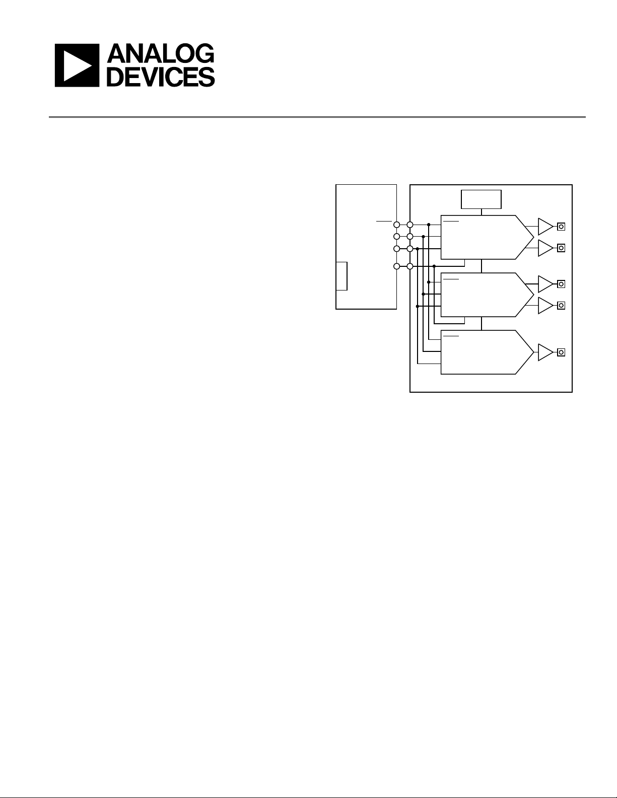
FUNCTIONAL BLOCK DIAGRAM
ADR01
REFERENCE
V
SDO
SDO
REF
AD5443
V
REF
AD5446
V
REF
AD5453
IOUT1
IOUT2
IOUT1
IOUT2
IOUT
SYNC
SCLK
SDI
SDO
SYNC
SCLK
SDI
SYNC
SCLK
SDI
SYNC
SCLK
SDI
GENERAL DESCRIPTION
The AD5443, AD5446 and AD54531 are CMOS 12-, 14-, and
14-bit, current output, digital-to-analog converters (DACs).
The AD5443 operates from a 3 V to 5.5 V power supply, while
the AD5446 and AD5453 operate from a single 2.5 V to 5.5 V
power supply. These devices are well suited for portable batterypowered and applications such as waveform generation and analog
processing.
Because of the CMOS submicron manufacturing process, these
parts offer excellent 4-quadrant multiplication characteristics of
10 MHz for the AD5443 and up to 12 MHz for the AD5446 and
AD5453 DACs.
These DACs use a double-buffered, 3-wire serial interface that
is compatible with SPI, QSPI™, MICROWIRE™, and most DSP
interface standards. On power-up, the internal shift register and
latches are filled with 0s, and the DAC output is at zero scale. In
addition for the AD5443 and AD5446, a serial data out pin
(SDO) allows for daisy-chaining when multiple packages are
used. Data readback allows the user to read the contents of the
DAC register via the SDO pin.
EVAL-AD5443/AD5446/AD5453SDZ
Figure 1.
The applied external reference input voltage (V
) determines
REF
the full-scale output current. An integrated feedback resistor
(R
) provides temperature tracking and full-scale voltage output
FB
when combined with an external current-to-voltage precision
amplifier.
The AD5443 and AD5446 are available in small 10-lead MSOP
packages, while the AD5453 is available in small 8-lead TSOT,
MSOP packages, also comes in 8-lead LFCSP.
The EVAL-AD5443SDZ/EVAL-AD5446SDZ/EVAL-AD5453SDZ
board is used in conjunction with the EVAL-SDP-CB1Z system
demonstration platform (SDP) board available from Analog
Devices, Inc., which is purchased separately from the evaluation
board. The USB-to-SPI communication to the DAC is completed
using this Blackfin®-based demonstration board.
10226-001
PLEASE SEE THE LAST PAGE FOR AN IMPORTANT
WARNING AND LEGAL TERMS AND CONDITIONS.
Rev. 0 | Page 1 of 12
Page 2

UG-327 Evaluation Board User Guide
TABLE OF CONTENTS
Features.............................................................................................. 1
Applications....................................................................................... 1
Functional Block Diagram .............................................................. 1
General Description ......................................................................... 1
Revision History ............................................................................... 2
Evaluation Board Software.............................................................. 3
Installing the Software ................................................................. 3
Running the Software .................................................................. 3
REVISION HISTORY
4/12—Revision 0: Initial Version
Using the Evaluation Board Software .............................................4
Example 1 .......................................................................................4
Example 2 .......................................................................................4
Example 3 .......................................................................................5
Evaluation Board Schematics and Artwork...................................6
Schematics......................................................................................6
Evaluation Board Layout ........................................................... 10
Related Links............................................................................... 11
Rev. 0 | Page 2 of 12
Page 3
Evaluation Board User Guide UG-327
EVALUATION BOARD SOFTWARE
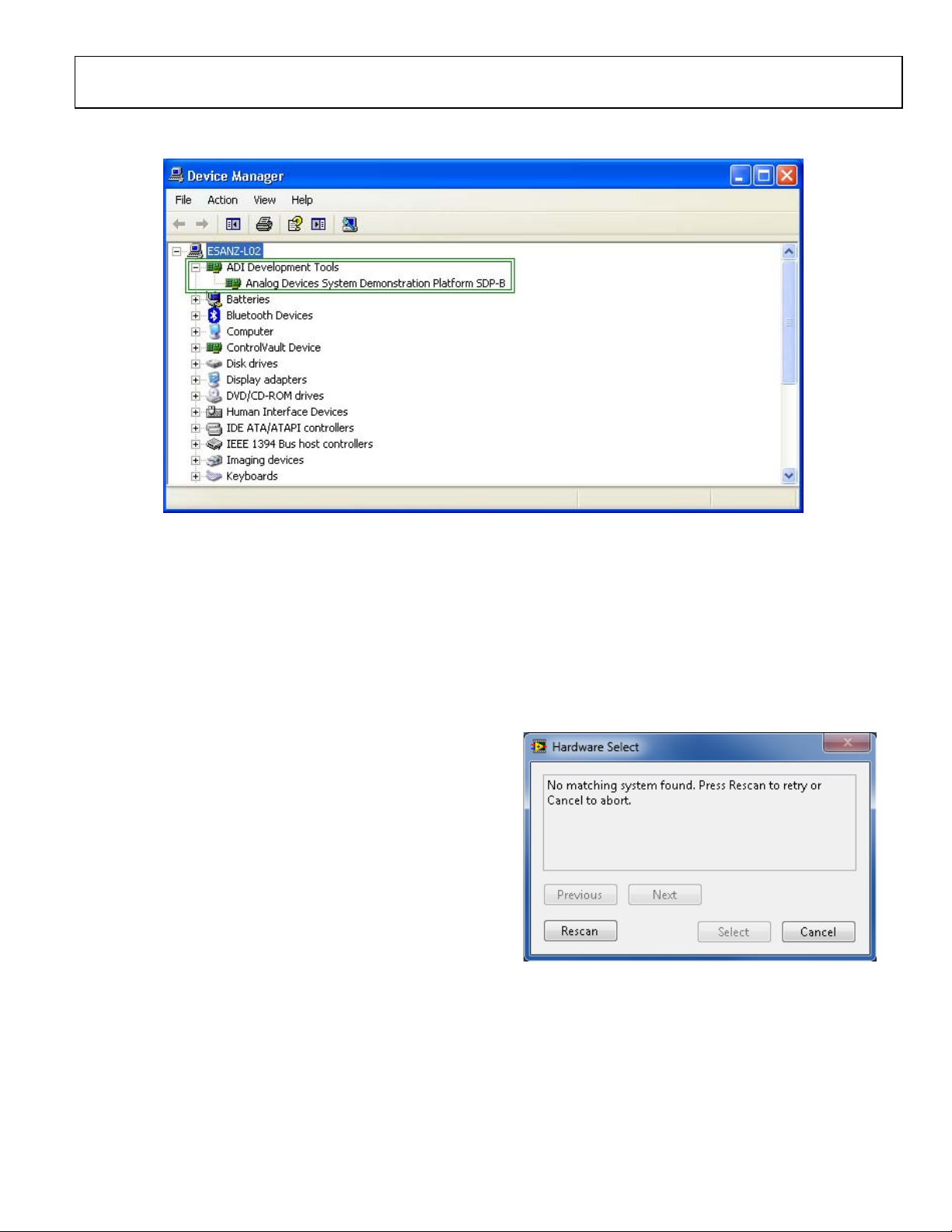
Figure 2. Device Manager Showing the SDP Board Connected
10226-002
INSTALLING THE SOFTWARE
The EVAL-AD5443SDZ/EVAL-AD5446SDZ/EVAL-AD5453SDZ
evaluation kit includes the software and drivers on CD. To install
the software, follow these steps:
1. Install the software before connecting the SDP board to the
USB port of the PC.
2. Start the Windows® operating system and insert the
EVAL-AD5443SDZ/EVAL-AD5446SDZ/EVAL-AD5453SDZ
evaluation kit CD.
3. Download the EVAL-AD5443SDZ/EVAL-AD5446SDZ/
EVAL-AD5453SDZ LabVIEW™ software. The correct driver,
SDPDriversNET, for the SDP board should download
automatically after LabVIEW is downloaded, supporting
both 32- and 64-bit systems. However, if the drivers do not
download automatically, the driver executable file can also be
found in the Program Files/Analog Devices folder. Follow
the on-screen prompts to install it.
4. After installation of the software and drivers is complete,
plug the EVAL-AD5443SDZ/EVAL-AD5446SDZ/EVAL-
AD5453SDZ into the SDP board and the SDP board into
the PC using the USB cable included in the box.
5. When the software detects the evaluation board, proceed
through any dialog boxes that appear to finalize the
installation (Found New Hardware Wizard/Install the
Software Automatically and so on).
RUNNING THE SOFTWARE
To run the evaluation board program, do the following:
1. Click Start/All Programs/Analog Devices/EVAL-
AD5443SDZ/EVAL-AD5446SDZ/EVAL-AD5453SDZ).
2. If the SDP board is not connected to the USB port when
the software is launched, a connectivity error displays (see
Figure 3). Simply connect the evaluation board to the USB
port of the PC, wait a few seconds, click Rescan, and follow
the instructions.
Figure 3. Connectivity Error (see Step 2)
10226-003
Rev. 0 | Page 3 of 12
Page 4
UG-327 Evaluation Board User Guide
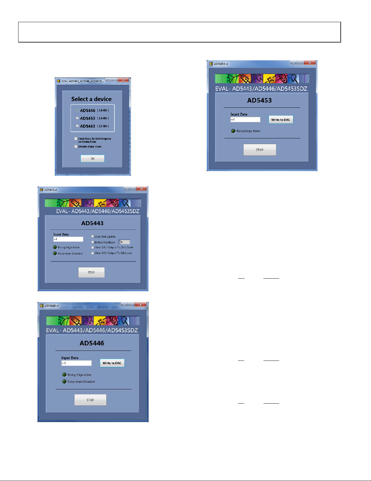
USING THE EVALUATION BOARD SOFTWARE
Once the software is launched, the main window pops up (see
Figure 4).
10226-007
10226-004
Figure 4. Main Window
Figure 7. AD5453 Evaluation Software Window
EXAMPLE 1
Select the AD5453 part from the main window. Tick the Clock
Data To Shift Register on Rising Edge box, and click the OK
button. The AD5453 Evaluation Software Window should appear.
The LED indicator with the Rising Edge Active label should be
light indicating the actual functionality mode (see Figure 5).
Enter Data 0x2000 (half scale) in the Input Data control and
click the Writ e to DAC button. Data is clocked on the rising
edge instead of the falling edge (by default). There is no loss of
data; therefore, the output shows the expected −5 V value. The
only change is the way the data is clocked.
D
VV
REF
n
2
Figure 5. AD5443 Evaluation Software Window
OUT
10226-005
EXAMPLE 2
Select the AD5446 part from the main window and click the
OK button. The AD5446 Evaluation Software Window should
appear. Enter Data 0x3FFF (full scale) in the Input Data control
and click the Wri te to DAC button. The output shows −10 V, and
because this write was the first action on the DAC after powering
up, the data on the SDO pin is not taken into account because
the data is not given any information.
D
VV
OUT
REF
n
2
Write Data 0x1000 (quarter scale) to the DAC. The output changes
its voltage from −10 V to −2.5 V, and the previous data written
to the part will appear on the SDO pin (in this example, −10 V).
D
VV
OUT
10226-006
Figure 6. AD5446 Evaluation Software Window
To finish evaluating the part, push the
To disable daisy-chain mode, tick the
Main Window after launching the application and before
in the
clicking the
Disabled
Rev. 0 | Page 4 of 12
REF
n
2
OK button. The LED indicator with the Daisy-chain
label will be light indicating the functionality mode.
10
10
10
8,192
16,384
383,16
384,16
383,16
384,16
V5
−=×−=×−=
−=×−=×−=
V
10
−=×−=×−=
V
10
STOP button.
Disable Daisy-chain box
Page 5

Evaluation Board User Guide UG-327
EXAMPLE 3
Select the AD5443 part from the Main Window and click the OK
button. The
Enter Data 0x800 (half scale) in the
select
Select
AD5443 Evaluation Software Window should appear.
Input Data control and
Load And Update. The output shows the expected −5 V value.
OUT
D
VV
REF
n
2
10
048,2
096,4
V
5
−=×−=×−=
Clear DAC Output To Zero Scale to get a voltage value
of 0 V on the output.
To put the part in three-quarter scale, write 0xBFD in the
Data
control and select Load And Update.
10
069,3
−=×−=×−=
V
096,4
5.7
Initiate
D
VV
OUT
REF
n
2
To verify the data in the DAC register is correct, select
Readback
and the indicator window beside this option shows
−7.5 V.
Input
Rev. 0 | Page 5 of 12
Page 6

UG-327 Evaluation Board User Guide
EVALUATION BOARD SCHEMATICS AND ARTWORK
SCHEMATICS
10226-015
Testpoints
Board ID EEPROM (24LC32)must be on I2Cbus 0,
8
7WP6
5
SCL
VCC
SDA
U1
24LC32
VSS
1A02A13A24
100K
DNP
3.3V
R3
R2
100K
R1
75
74
73
72
71NC70NC69
68NC67NC66NC65NC64NC63
62
61
GND
GND
BMODE1
UART_TX
SDP
STANDARD
CONNECTOR
J1
UART_RX58GND57NC56EEPROM_A055NC54NC53NC52GND51NC50NC49TMR_C48TMR_A47GPIO646GND45GPIO444GPIO243GPIO042SCL_141SDA_140GND39SPI_SEL1/SPI_SS38SPI_SEL_C37SPI_SEL_B36GND35SPORT_INT34SPORT_DT333SPORT_DT232SPORT_DT131SPORT_DR130SPORT_DR229SPORT_DR328GND27PAR_FS126PAR_FS325PAR_A124PAR_A323GND22PAR_CS21PAR_RD20PAR_D119PAR_D318PAR_D517GND16PAR_D715PAR_D914PAR_D1 113PAR_D1 312PAR_D1 411GND10PAR_D1 79PAR_D1 98PAR_D2 17PAR_D2 36GND5USB_VBU S4GND3GND2NC1VIN
RESET_IN
59
60
BMODE1:Pull up with a 10Kresistor to set SDPtobo ot from a SPI FLASHon the daughte rboard
GPIO7
TMR_B
TMR_D
TIMERS
*
Main I2C bus (Connected to blackfin TWI - Pull up resistors not required)
SCLK
SDIN
/SYNC
91
90
89
88
87
86
85
84
82
81
80
79
78
GND
GND
GND
SCL_0
GPIO177GPIO376GPIO5
SDA_0
SPI_CLK
SPI_MOSI83SPI_MISO
SPI_ SEL_A
SPORT_TFS
SPORT_RFS
SPORT_DT0
SPORT_DR0
SPORT_TS C LK
SPI
I2C
GENERAL
INPUT/OUT PUT
SPORT
*
/SYNC /SYNC1 SCLK/SYNC2 SDIN
R8
99
98
97
95
94
93
92
GND
GND
PAR_A296PAR_A0
PAR_INT
PAR_FS2
PAR_CLK
SPORT_RSCLK
***
R7
R6
SDO_AD5443 SDO_AD5446
/SYNC /SYNC1 /SYNC2 SCLK SDIN
108
107
106
105
104
103
102
101
100
GND
PAR_D8
PAR_D6
PAR_D4
PAR_D2
PAR_D0
PAR_WR
PAR_D10
PORT
PARALLEL
SDO_AD5443 SDO_AD5446
3.3V
VIO: USEto set IO voltage max draw20mA
120NC119NC118
117
116
115
114
113
112
111
110
109
GND
GND
GND
GND
PAR_D22
PAR_D20
PAR_D18
PAR_D16
PAR_D15
PAR_D12
***
*
VIO(+3.3V)
*NC on BLACKFIN SDP
***
*
/SYNC1
/SYNC2
SDO_AD5443
S2
INDS
ADG701BRJZ
4
2
5
3.3V
S DO selector
3
GND
VDD
1
SDO_AD5446
S1
IN
ADG702BRJZ
S
3.3V
GND
VDD
D
USB_VBUS
VIN: Use this pin to power the SDP requires 5V 200mA
Figure 8. EVAL-AD5443SDZ/EVAL-AD5446SDZ/EVAL-AD5453SDZ Schematic, SDP Connector
Rev. 0 | Page 6 of 12
Page 7

Evaluation Board User Guide UG-327
J5
10226-016
VOUT2
VOUT2
+
0.1uF
C18
C19
C17
4V-7
VSS
AD8065 AR
4.7pF
10uF
0.1uF
10
RFB
10uF
R5
C16
3.3V
+
C15
8
VDD
U6
1
6
-
IOUT12IOUT2
10uF
0.1uF
+
C20
V+
3+2
C21
U8
VDD
LK3
C24
0.1uF
VREF
J4
VREF
VREF
3
9
GND
VREF
4
2
VOUT
GND
+VIN
TRIM
ADR01BKSZ_ U7
5
3
0.1uF
C23
VDD
+
C22
10uF
SCLK5SDIN6SYNC7SDO/LDAC
4
SCLK
SDIN
/SYNC2
SDO_AD544 3
AD5426_ AD5432_AD544 3
J6-1
J6-2
J6-3
VDD
VSS
Figure 9. EVAL-AD5443SDZ/EVAL-AD5446SDZ/EVAL-AD5453SDZ Schematic, AD5443 DAC
Rev. 0 | Page 7 of 12
Page 8

UG-327 Evaluation Board User Guide
J3
10226-017
VOUT1
VOUT1
+
0.1uF
C10
C11
10uF
VSS
AD8065AR
C14
4.7pF
R4
C9
10uF
3.3V
+
C8
0.1uF
6
4V-7
V+
3+2
U5
C12
10uF
0.1uF
+
C13
VDD
VREF
8
10
RFB
VDD
U4
SCLK5SDIN6SYNC7SDO
4
SCLK
SDIN
1
IOUT12IOUT2
/SYNC1
3
9
GND
VREF
AD5444/AD5446
SDO_AD5446
Figure 10. EVAL-AD5443SDZ/EVAL-AD5446SDZ/EVAL-AD5453SDZ Schematic, AD5446 DAC
Rev. 0 | Page 8 of 12
Page 9

Evaluation Board User Guide UG-327
J2
VOUT
VOUT_
+
0.1uF
C4
C5
10uF
VSS
AD8065AR
C3
1.8pF
C2
10uF
3.3V
+
C1
0.1uF
6
4V-7
V+
3+2
10uFC70.1uF
+
C6
U3
VDD
10226-018
VREF
1
3
VDD
U2
SCLK
6
SCLK
8
RFB
IOUT1
SDIN
SYNC
5
4
SDIN
/SYNC
2
7
GND
VREF
AD5450_1_2_ 3
Figure 11. EVAL-AD5443SDZ/EVAL-AD5446SDZ/EVAL-AD5453SDZ Schematic, AD5453 DAC
Rev. 0 | Page 9 of 12
Page 10

UG-327 Evaluation Board User Guide
EVALUATION BOARD LAYOUT
10226-012
Figure 12. EVAL-AD5443SDZ/EVAL-AD5446SDZ/EVAL-AD5453SDZ Silkscreen
Figure 13. EVAL-AD5443SDZ/EVAL-AD5446SDZ/EVAL-AD5453SDZ Component Side
10226-013
Rev. 0 | Page 10 of 12
Page 11

Evaluation Board User Guide UG-327
10226-014
Figure 14. EVAL-AD5443SDZ/EVAL-AD5446SDZ/EVAL-AD5453SDZ Solder Side
RELATED LINKS
Resource Description
AD5443 Product Page, AD5443 High Bandwidth CMOS 12-Bit Serial Interface Multiplying D/A Converter
AD5446 Product Page, AD5446 14-Bit High Bandwidth Multiplying DAC with Serial Interface
AD5453 Product Page, AD5453 14-Bit High Bandwidth Multiplying DACs with Serial Interface
ADR01 Product Page, ADR01 Ultracompact, Precision 10.0 V Voltage Reference
AD8065 Product Page, AD8065 High Performance, 145 MHz FastFET™ Op Amp
EVAL-SDP-CB1Z Product Page, System Demonstration Platform-Blackfin
Rev. 0 | Page 11 of 12
Page 12

UG-327 Evaluation Board User Guide
NOTES
Legal Terms and Conditions
By using the evaluation board discussed herein (together with any tools, components documentation or support materials, the “Evaluation Board”), you are agreeing to be bound by the terms and conditions
set forth below (“Agreement”) unless you have purchased the Evaluation Board, in which case the Analog Devices Standard Terms and Conditions of Sale shall govern. Do not use the Evaluation Board until you
have read and agreed to the Agreement. Your use of the Evaluation Board shall signify your acceptance of the Agreement. This Agreement is made by and between you (“Customer”) and Analog Devices, Inc.
(“ADI”), with its principal place of business at One Technology Way, Norwood, MA 02062, USA. Subject to the terms and conditions of the Agreement, ADI hereby grants to Customer a free, limited, personal,
temporary, non-exclusive, non-sublicensable, non-transferable license to use the Evaluation Board FOR EVALUATION PURPOSES ONLY. Customer understands and agrees that the Evaluation Board is provided
for the sole and exclusive purpose referenced above, and agrees not to use the Evaluation Board for any other purpose. Furthermore, the license granted is expressly made subject to the following additional
limitations: Customer shall not (i) rent, lease, display, sell, transfer, assign, sublicense, or distribute the Evaluation Board; and (ii) permit any Third Party to access the Evaluation Board. As used herein, the term
“Third Party” includes any entity other than ADI, Customer, their employees, affiliates and in-house consultants. The Evaluation Board is NOT sold to Customer; all rights not expressly granted herein, including
ownership of the Evaluation Board, are reserved by ADI. CONFIDENTIALITY. This Agreement and the Evaluation Board shall all be considered the confidential and proprietary information of ADI. Customer may
not disclose or transfer any portion of the Evaluation Board to any other party for any reason. Upon discontinuation of use of the Evaluation Board or termination of this Agreement, Customer agrees to
promptly return the Evaluation Board to ADI. ADDITIONAL RESTRICTIONS. Customer may not disassemble, decompile or reverse engineer chips on the Evaluation Board. Customer shall inform ADI of any
occurred damages or any modifications or alterations it makes to the Evaluation Board, including but not limited to soldering or any other activity that affects the material content of the Evaluation Board.
Modifications to the Evaluation Board must comply with applicable law, including but not limited to the RoHS Directive. TERMINATION. ADI may terminate this Agreement at any time upon giving written notice
to Customer. Customer agrees to return to ADI the Evaluation Board at that time. LIMITATION OF LIABILITY. THE EVALUATION BOARD PROVIDED HEREUNDER IS PROVIDED “AS IS” AND ADI MAKES NO
WARRANTIES OR REPRESENTATIONS OF ANY KIND WITH RESPECT TO IT. ADI SPECIFICALLY DISCLAIMS ANY REPRESENTATIONS, ENDORSEMENTS, GUARANTEES, OR WARRANTIES, EXPRESS OR IMPLIED, RELATED
TO THE EVALUATION BOARD INCLUDING, BUT NOT LIMITED TO, THE IMPLIED WARRANTY OF MERCHANTABILITY, TITLE, FITNESS FOR A PARTICULAR PURPOSE OR NONINFRINGEMENT OF INTELLECTUAL
PROPERTY RIGHTS. IN NO EVENT WILL ADI AND ITS LICENSORS BE LIABLE FOR ANY INCIDENTAL, SPECIAL, INDIRECT, OR CONSEQUENTIAL DAMAGES RESULTING FROM CUSTOMER’S POSSESSION OR USE OF
THE EVALUATION BOARD, INCLUDING BUT NOT LIMITED TO LOST PROFITS, DELAY COSTS, LABOR COSTS OR LOSS OF GOODWILL. ADI’S TOTAL LIABILITY FROM ANY AND ALL CAUSES SHALL BE LIMITED TO THE
AMOUNT OF ONE HUNDRED US DOLLARS ($100.00). EXPORT. Customer agrees that it will not directly or indirectly export the Evaluation Board to another country, and that it will comply with all applicable
United States federal laws and regulations relating to exports. GOVERNING LAW. This Agreement shall be governed by and construed in accordance with the substantive laws of the Commonwealth of
Massachusetts (excluding conflict of law rules). Any legal action regarding this Agreement will be heard in the state or federal courts having jurisdiction in Suffolk County, Massachusetts, and Customer hereby
submits to the pers onal jurisdiction and venu e of such courts. The United Nations Conventi on on Contracts for the Internation al Sale of Goods shall not apply to this Agreement and is expressly disclaimed.
©2012 Analog Devices, Inc. All rights reserved. Trademarks and
registered trademarks are the property of their respective owners.
UG10226-0-4/12(0)
Rev. 0 | Page 12 of 12
 Loading...