

Page 1
Evaluation Board User Guide
UG-215
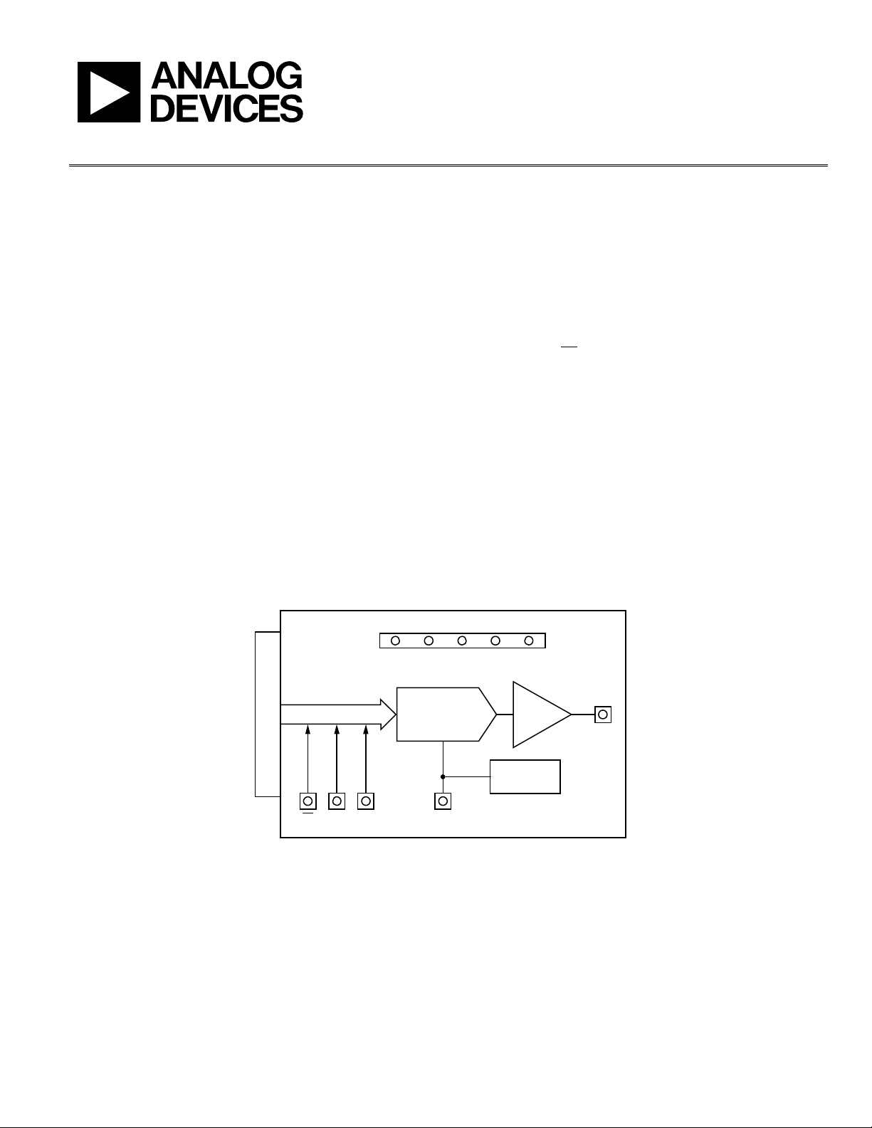
DVDD DGND VSS AGND
VDD
AD5543/AD5553
16-/14-BIT DAC
AD8065
I-TO-V
V
OUT
V
REF
ADR435
REFERENCE
CONNECTOR TO EVAL-SDP-CB1Z
SDIN SCLKCS
09485-001
One Technology Way • P. O. Box 9106 • Norwood, MA 02062-9106, U.S.A. • Tel: 781.329.4700 • Fax: 781.461.3113 • www.analog.com
Evaluating the AD5543 Current Output/Serial Input DAC
FEATURES
Full-featured evaluation board for the AD5543
Graphic user interface software for board control and data
analysis
Connector to E VAL-SDP-CB1Z system development platform
board
Various power supply options
APPLICATIONS
Automatic test equipment
Instrumentation
Digitally controlled calibration
Industrial control PLCs
GENERAL DESCRIPTION
The AD5543 is a precision, 16-bit, low power, current output,
small form factor, digital-to-analog converter (DAC). It is
designed to operate from a single 5 V supply with a ±10 V
multiplying reference.
FUNCTIONAL BLOCK DIAGRAM
The applied external reference, V
output current. An internal feedback resistor (RFB) facilitates
the R-2R and temperature tracking for voltage conversion when
combined with an external op amp.
A serial data interface offers high speed, 3-wire, microcontrollercompatible inputs using serial data input (SDI), clock (CLK),
and chip select (
CS
).
The AD5543 is packaged in ultracompact (3 mm × 4.7 mm)
8-lead MSOP and 8-lead SOIC packages.
The E VA L -AD5543/53SDZ board is used in conjunction with
the EVAL -SDP-CB1Z system development platform (SDP) board
available from Analog Devices, Inc., which is purchased separately from the evaluation board. The USB-to-SPI communication
to the AD5543 is completed using this Blackfin®-based development board. The software offers a waveform generator.
The EVAL-AD5543/53SDZ can also be used for the AD5553 by
changing the number of bits written (14 bits) in the input.
, determines the full-scale
REF
PLEASE SEE THE LAST PAGE FOR AN IMPORTANT
WARNING AND LEGAL TERMS AND CONDITIONS.
Figure 1.
Rev. A | Page 1 of 12
Page 2

UG-215 Evaluation Board User Guide
TABLE OF CONTENTS
Features .............................................................................................. 1
Applications ....................................................................................... 1
General Description ......................................................................... 1
Functional Block Diagram .............................................................. 1
Revision History ............................................................................... 2
REVISION HISTORY
2/12—Rev. 0 to Rev. A
Changes to Level Set Section ........................................................... 4
Replaced Evaluation Board Schematics and Artwork Section ... 7
11/10—Revision 0: Initial Version
Evaluation Board Software ...............................................................3
Quick Start Procedure ..................................................................3
AD5543 Evaluation Software Window ......................................4
Evaluation Board Schematics and Artwork ...................................7
Evaluation Board Layout ..............................................................9
Rev. A | Page 2 of 12
Page 3
Evaluation Board User Guide UG-215
09485-002
EVALUATION BOARD SOFTWARE
QUICK START PROCEDURE
To get started, do the following:
1. Load and install the software CD.
2. Plug in the SDP board. The Found New Hardware Wizard
dialog box opens, which allows you to install the software
automatically.
3. Load the software for the SDP board. Click the Start
button on the bottom left corner of your screen, then All
Programs, then AD5543, and finally select the
SDP32NET executable for the SDP board.
4. Connect the SDP board to the AD5543 evaluation board,
and plug in the external power supply.
5. Load the AD5543 software. Click Start, then All
Programs, then Analog Devices, and finally AD5543.
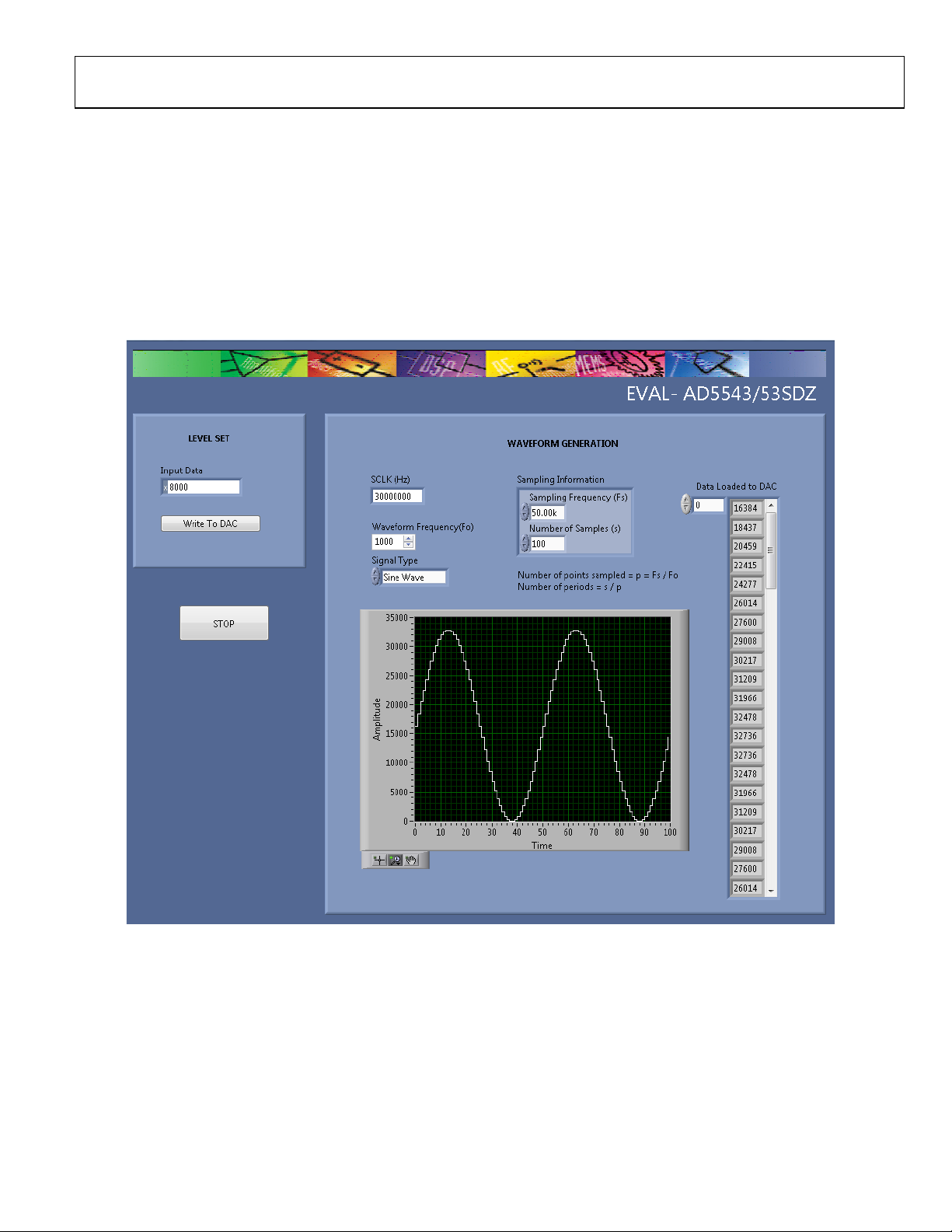
Figure 2. AD5543 Evaluation Software
Rev. A | Page 3 of 12
Page 4

UG-215 Evaluation Board User Guide
REF
N
OUT
V
D
V ×−= )1
2
(
SampledPointsofNumber
samplesofNumber
PeriodsofNumber =
40
Hz500
Hz000,20
==SampledPointsofNumber
2
40
80
==PeriodsofNumber
2000
Hz500
Hz000,000,1
==SampledPointsofNumber
1
2000
2000
==PeriodsofNumber
AD5543 EVALUATION SOFTWARE WINDOW
LEVEL SET
The LEVEL SET section in the AD5543 evaluation software
allows you to choose the amplitude for the waveform depending
on the code entered in the Input Data box. Click the Write To
DAC button to load the code. Being a 16-Bit DAC, the relationship between the code entered and the voltage in the output is
as follows:
where:
N = 16 bits.
V
= 5 V.
REF
D is the code introduced in decimal (0 to 32,767).
Waveform Generation
The WAVEFORM GENERATION section allows you to
control the different frequencies and features in the waveform
generation, including
• SCLK: clock input frequency (30 MHz default value).
• Waveform Frequency (Fo).
• Signal Type: dc signal (default), sawtooth, sine, triangle,
and square wave options.
• Sampling Information includes the two following features:
• Sampling Frequency (Fs): to avoid the aliasing effect,
it is necessary to choose a frequency that is at least
twice the value of the waveform frequency. The
number of points sampled is calculated as follows:
SampledPointsofNumber =
FrequencySampling
FrequencyWaveform
• Number of Samples (s): this constant allows you to
show in a graph a determined number of periods
depending on its value. The maximum number of
samples is 32,768.
• Data Loaded to DAC: the array contains the value of every
code where the waveform has been sampled.
• The graph shows each of the points contained in the array.
Example 1
1. Power on the board.
2. Start up the software.
3. Select the default 30 MHz clock frequency.
4. Select a waveform frequency of 500 Hz and Sine Wav e as
the signal type to show (dc signal is the default).
5. Select a sampling frequency of 20 kHz and 80 for the
number of samples.
6. Write the Code FFFF to show full scale.
7. Click Write To DAC.
The waveform obtained from the values entered shows two
periods and the 40 samples per period (see Figure 3). The code
of each sample is loaded in the array on the right side.
Click the STOP button to end the execution of the software.
Example 2
For a sharper waveform, the sampling frequency and the
number of samples must be raised according to the frequency.
The next example (see Figure 4) shows this relationship, where
the sampling frequency value is changed to 1 MHz and the
number of samples is 2000.
Rev. A | Page 4 of 12
Page 5

Evaluation Board User Guide UG-215
09485-003
Figure 3. Example 1
Rev. A | Page 5 of 12
Page 6

UG-215 Evaluation Board User Guide
09485-004
Figure 4. Example 2
Rev. A | Page 6 of 12
Page 7

Evaluation Board User Guide UG-215
09485-005
VREF
VOUT
Op-Amp + Reference Supply
DAC + Vin for SDP
SCLK
SDIN
AGND
+
C1
10uF
C2
0.1uF
VREF
+
C8
10uF
C9
0.1uF
C10
0.1uF
J3
C3
5.6pF
VOUT
2
-
3
+
6
OP
4
V-
7
V+
8
DIS
U3
+
C4
10uF
C5
0.1uF
+
C6 10uF
C7
0.1uF
J4
5
IOUT
3
RFB
6
AGND
1
SCLK
2
SDIN
8
CS
CS
CS
7
VDD
4
VREF
U1
AD5543_53
2
+VIN
5
TRIM
6
VOUT
4
GND
U2
ADR435
J1-1
J1-5
J1-4
J1-3
J1-2
LK1
DVDD
VDD
VDD
VSS
VSS
VDD
DVDD
SCLK
SDIN
DGND
EVALUATION BOARD SCHEMATICS AND ARTWORK
Figure 5. AD5543 Schematic Part A
Rev. A | Page 7 of 12
Page 8

UG-215 Evaluation Board User Guide
09485-006
VIN: Use this pin to power the SDPrequires4-7V 200mA
VIO: USE to set IO voltage max draw 20mA
Board ID EEPROM (24LC64) must be on I2C bus 0, address is at userdiscretion
I2Cbus 1 is commonacross bothconnectors on SDP- Pull up resistors required
BMODE1: Pull up with a 10Kresistor to set SDP to boot from a SPI FLASH on the daughter board
(connected toblackfin GPIO- use I2C_0 first)
MainI2C bus(Connected to blackfin TWI - Pull up resistors not required)
CONNECTOR
STANDARD
SDP
PARALLEL
PORT
SPORT
SPI
I2C
GENERAL
INPUT/OUTPUT
TIMERS
*
*
*
*
*
*
*
*
*
*
*
*
*
*NC on BLACKFINSDP
120
NC
119
NC
118
GND
117
GND
116
VIO(+3.3V)
115
GND
114
PAR_D22
113
PAR_D20
112
PAR_D18
111
PAR_D16
110
PAR_D15
109
GND
108
PAR_D12
107
PAR_D10
106
PAR_D8
105
PAR_D6
104
GND
103
PAR_D4
102
PAR_D2
101
PAR_D0
100
PAR_WR
99
PAR_INT
98
GND
97
PAR_A2
96
PAR_A0
95
PAR_FS2
94
PAR_CLK
93
GND
92
SPORT_RSCLK
91
SPORT_DR0
90
SPORT_RFS
89
SPORT_TFS
88
SPORT_DT0
87
SPORT_TSCLK
86
GND
85
SPI_SEL_A
84
SPI_MOSI
83
SPI_MISO
82
SPI_CLK
81
GND
80
SDA_0
79
SCL_0
78
GPIO1
77
GPIO3
76
GPIO5
75
GND
74
GPIO7
73
TMR_B
72
TMR_D
71
NC
70
NC
69
GND
68
NC
67
NC
66
NC
65
NC
64
NC
63
GND
62
UART_TX
61
BMODE1
60
RESET_IN
59
UART_RX
58
GND
57
NC
56
NC
55
NC
54
NC
53
NC
52
GND
51
NC
50
NC
49
TMR_C
48
TMR_A
47
GPIO6
46
GND
45
GPIO4
44
GPIO2
43
GPIO0
42
SCL_1
41
SDA_1
40
GND
39
SPI_SEL1/SPI_SS
38
SPI_SEL_C
37
SPI_SEL_B
36
GND
35
SPORT_INT
34
SPORT_DT3
33
SPORT_DT2
32
SPORT_DT1
31
SPORT_DR1
30
SPORT_DR2
29
SPORT_DR3
28
GND
27
PAR_FS1
26
PAR_FS3
25
PAR_A1
24
PAR_A3
23
GND
22
PAR_CS
21
PAR_RD
20
PAR_D1
19
PAR_D3
18
PAR_D5
17
GND
16
PAR_D7
15
PAR_D9
14
PAR_D11
13
PAR_D13
12
PAR_D14
11
GND
10
PAR_D17
9
PAR_D19
8
PAR_D21
7
PAR_D23
6
GND
5
USB_VBUS
4
GND
3
GND
2
NC
1
VIN
J2
1
A0
2
A1
3
A2
4
VSS
8
VCC
7
WP
6
SCL
5
SDA
U4
24LC64
USB_VBUS
3.3V_BF
SCLK
SDIN
/CS
START
3.3V_BF
STATUS
Figure 6. AD5543 Schematic Part B
Rev. A | Page 8 of 12
Page 9

Evaluation Board User Guide UG-215
09485-007
09485-008
09485-009
EVALUATION BOARD LAYOUT
Figure 7. Silkscreen Top
Figure 8. Top Side
Figure 9. Bottom Side
Rev. A | Page 9 of 12
Page 10

UG-215 Evaluation Board User Guide
Resource
Description
RELATED LINKS
AD5543 Product Page, AD5543 16-Bit DAC in µSOIC-8 Package
AD5553 Product Page, AD5553 14-Bit DAC in µSOIC-8 Package
ADR435 Product Page, ADR435 Ultralow Noise XFET® Voltage References with Current Sink and Source Capability
AD8065 Product Page, AD8065 High Performance, 145 MHz FastFET™ Op Amp
Rev. A | Page 10 of 12
Page 11

Evaluation Board User Guide UG-215
NOTES
Rev. A | Page 11 of 12
Page 12

UG-215 Evaluation Board User Guide
tion Board for any other purpose. Furthermore, the license granted is expressly made subject to the following additional
NOTES
ESD Caution
ESD (electrostatic discharge) sensitive device. Charged devices and circuit boards can discharge without detection. Although this product features patented or proprietary protection
circuitry, damage may occur on devices subjected to high energy ESD. Therefore, proper ESD precautions should be taken to avoid performance degradation or loss of functionality.
Legal Terms and Conditions
By using the evaluation board discussed herein (together with any tools, components documentation or support materials, the “Evaluation Board”), you are agreeing to be bound by the terms and conditions
set forth below (“Agreement”) unless you have purchased the Evaluation Board, in which case the Analog Devices Standard Terms and Conditions of Sale shall govern. Do not use the Evaluation Board until you
have read and agreed to the Agreement. Your use of the Evaluation Board shall signify your acceptance of the Agreement. This Agreement is made by and between you (“Customer”) and Analog Devices, Inc.
(“ADI”), with its principal place of business at One Technology Way, Norwood, MA 02062, USA. S ubject to the terms and conditions of the Agreement, ADI hereby grants to Customer a free, limited, personal,
temporary, non-exclusive, non-sublicensable, non-transferable license to use the Evaluation Board FOR EVALUATION PURPOSES ONLY. Customer understands and agrees that the Evaluation Board is provided
for the sole and exclusive purpose referenced above, and agrees not to use the Evalua
limitations: Customer shall not (i) rent, lease, display, sell, transfer, assign, sublicense, or distribute the Evaluation Board; and (ii) permit any Third Party to access the Evaluation Board. As used herein, the term
“Third Party” includes any entity other than ADI, Customer, their employees, affiliates and in-house consultants. The Evaluation Board is NOT sold to Customer; all rights not expressly granted herein, including
ownership of the Evaluation Board, are reserved by ADI. CONFIDENTIALIT Y. This Agreement and the Evaluation Board shall all be considered the confidential and proprietary information of ADI. Customer may
not disclose or transfer any portion of the Evaluation Board to any other party for any reason. Upon discontinuation of use of the Evaluation Board or termination of this Agreement, Customer agrees to
promptly return the Evaluation Board to ADI. ADDITIONAL RESTRICTIONS. Customer may not disassemble, decompile or reverse engineer chips on the Evaluation Board. Customer shall inform ADI of any
occurred damages or any modifications or alterations it makes to the Evaluation Board, including but not limited to soldering or any other activity that affects the material content of the Evaluation Board.
Modifications to the Evaluation Board must comply with applicable law, including but not limited to the RoHS Directive. TERMINATION. ADI may terminate this Agreement at any time upon giving written notice
to Customer. Customer agrees to return to ADI the Evaluation Board at that time. LIMITATION OF LIABILITY. THE EVALUATION BOARD PROVIDED HEREUNDER IS PROVIDED “AS IS” AND ADI MAKES NO
WARRANTIES OR REPRES ENTATIONS OF ANY KIND WITH RESPECT TO IT. ADI SPECIFICALLY DISCLAIMS ANY REPRESENTATIONS, ENDORSEMENTS, GUARANTEES, OR WARRANTIES, E XPRESS OR IMPLIE D, RELATED
TO THE EVALUATION BOARD INCLUDING, BUT NOT LIMITED TO, THE IMPLIED WARRANTY OF MERCHANTABILITY, TITLE, FITNESS FOR A PARTICULAR PURPOSE OR NONINFRINGEMENT OF INTELLECTUAL
PROPERTY RIGHTS. IN NO EVENT WILL ADI AND ITS LICENSORS BE LIABLE FOR ANY INCIDENTAL, SPECIAL, INDIRECT, OR CONSEQUENTIAL DAMAGES RESULTING FROM CUSTOMER’S POSSESSION OR USE OF
THE EVALUATION BOARD, INCLUDING BUT NOT LIMITED TO LOST PROFITS, DELAY COSTS, LABOR COSTS OR LOSS OF GOODWILL. ADI’S TOTAL LIABILITY FROM AN Y AND ALL CAUSES SHALL BE LIMITED TO THE
AMOUNT OF ONE HUNDRED US DOLLARS ($100.00). EXPORT. Customer agrees that it will not directly or indirectly export the Evaluation Board to another country, and that it will comply with all applicable
United States federal laws and regulations relating to exports. GOVERNING LAW. This Agreement shall be governed by and construed in accordance with the substantive laws of the Commonwealth of
Massachusetts (excluding conflict of law rules). Any legal action regarding this Ag re ement will be heard in the state or federal cour ts having jurisdicti on in Suffolk County, Mass achusetts, and Customer h ereby
submits to the per sonal jurisdiction and venue of such courts. The United Nations Convention on Contracts for the International Sale of Goods shall not app ly to this Agreement and is expressl y disclaimed.
©2010–2012 Analog Devices, Inc. All rights reserved. Trademarks and
registered trademarks are the property of their respective owners.
UG09485-0-2/12(A)
Rev. A | Page 12 of 12
 Loading...