

Page 1
Evaluation Board User Guide
One Technology Way • P. O . Box 9106 • Norwood, MA 02062-9106, U.S.A. • Tel : 781.329.4700 • Fax : 781.461.3113 • www.analog.com
UG-186
User Guide for ADP322/ADP323 Evaluation Board
FEATURES
Bias voltage range (V
LDO input voltage range (V
Output current range: 0 mA to 200 mA per output
Output voltage accuracy: ±1%
Operating temperature range: −40°C to +125°C
): 2.5 V to 5.5 V
BIAS
IN1/VIN2
, V
): 1.8 V to 5.5 V
IN3
GENERAL DESCRIPTION
The ADP322/ADP323 evaluation board is used to demonstrate the
functionality of the ADP322/ADP323 series of linear regulators.
Simple device measurements, such as line and load regulation,
dropout voltage, and ground current, can be demonstrated with
two voltage supplies, a few voltmeters, current meters, and load
resistors.
For more details about the ADP322/ADP323 linear regulators,
see the ADP322/ADP323 data sheet.
EVALUATION BOARD
PLEASE SEE THE LAST PAGE FOR AN IMPORTANT
WARNING AND LEGAL TERMS AND CONDITIONS.
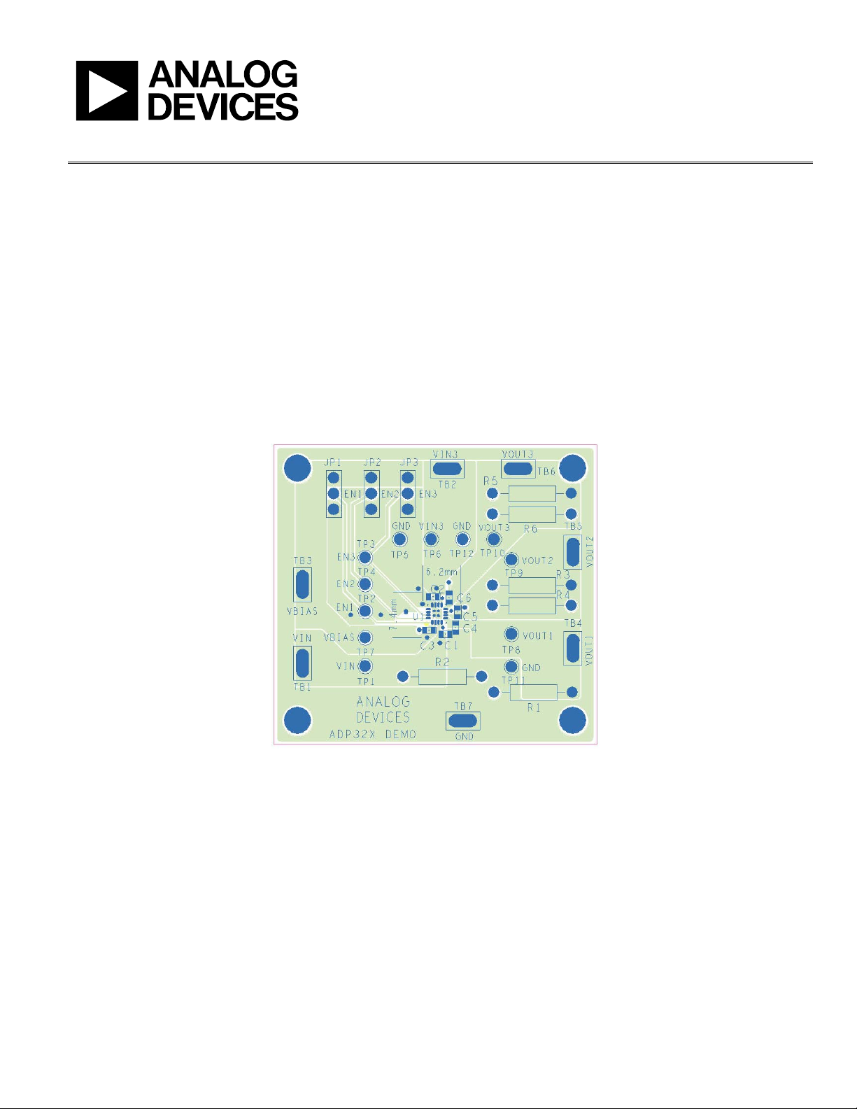
Figure 1. ADP322/ADP323 Evaluation Board
Rev. 0 | Page 1 of 12
9299-001
Page 2

UG-186 Evaluation Board User Guide
TABLE OF CONTENTS
Features.............................................................................................. 1
General Description ......................................................................... 1
Evaluation Board .............................................................................. 1
Revision History ............................................................................... 2
Evaluation Board Hardware and Schematic ................................. 3
Output Voltage Measurements ....................................................... 4
Line Regulation Measurements.................................................. 4
Load Regulation Measurements................................................. 5
REVISION HISTORY
10/10—Revision 0: Initial Version
Dropout Voltage Measurements..................................................5
Ground and Bias Current Measurements ......................................6
Ground Current Measurement....................................................6
Bias Current Measurement ..........................................................7
Printed Circuit Board Layout Considerations...............................8
Ordering Information.......................................................................9
Bill of Materials..............................................................................9
Related Links......................................................................................9
Rev. 0 | Page 2 of 12
Page 3
Evaluation Board User Guide UG-186
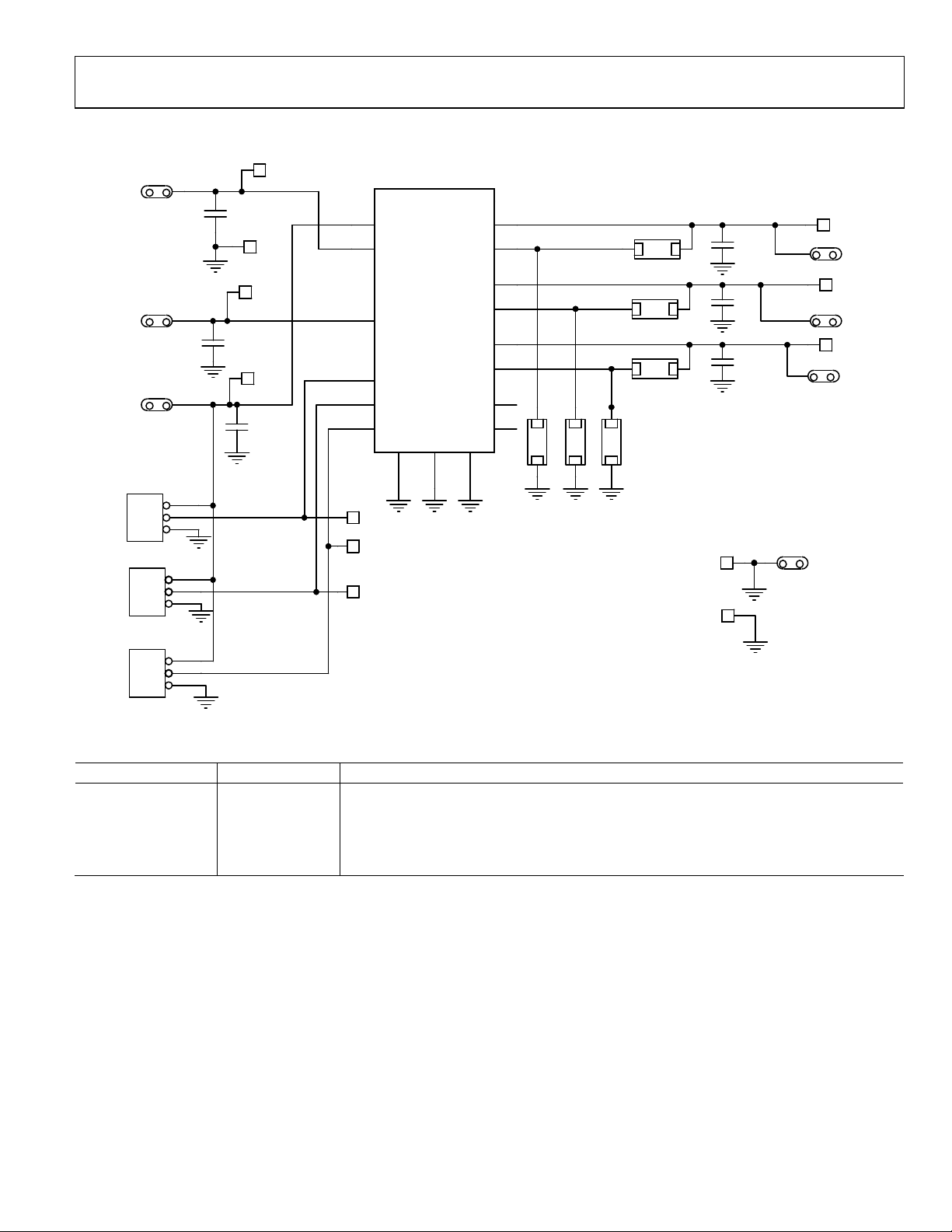
EVALUATION BOARD HARDWARE AND SCHEMATIC
1
1µF
1
C2
1
C1
1
EN1
EN3
VIN
TP5
TP6
TP7
VBIAS
C3
1µF
EN2
TP1
VIN3
U1
ADP322/ADP323
2
VBIAS
3
VIN1/VIN2
10
VIN3
1
EN1
16
EN2
15
EN3
NC
GND
11
12
1
TP2
1
TP3
1
TP4
VOUT1
FB1/NC
VOUT2
FB2/NC
VOUT3
FB3/NC
NC
NC
PAD
PAD
5
4
6
7
8
9
14
13
R2
RES
1 2
1 2
Figure 2. ADP322/ADP323 Evaluation Board Schematic
RES
R4
R1
1 2
R3
1 2
R5
1 2
2
R6
RES
1
RES
RES
RES
TP11
TP12
C4
1µF
C5
1µF
C6
1µF
1
VOUT1
VOUT2
VOUT3
1
TB7
1
1
1
TB4
TB5
TB6
GND
TP8
TP9
TP10
09299-002
TB1
TB2
TB3
JP1
1
2
3
HEADER_3
JP2
HEADER_3
JP3
HEADER_3
1µF
1
2
3
1
1
2
2
3
3
1
1
2
2
3
3
Table 1. Evaluation Board Hardware Components
Component Function Description
U11 Linear regulator ADP322/ADP323 low dropout linear regulator.
C1, C2, C3, C4, C5, C6 Input capacitor 1 μF input bypass capacitor, 0402 or 0603 case.
JP1, JP2, JP3 3-pin jumper These jumpers connect EN1, EN2, and EN3 to VBIAS for automatic startup.
R1, R2, R3, R4, R5, R6 Resistor
Resistors for setting output voltage for the ADP323, 0603 size. Short R1, R3, and R5 to connect
the output voltage to the feedback input for the ADP322.
1
Component varies depending on the evaluation board type ordered.
Rev. 0 | Page 3 of 12
Page 4
UG-186 Evaluation Board User Guide
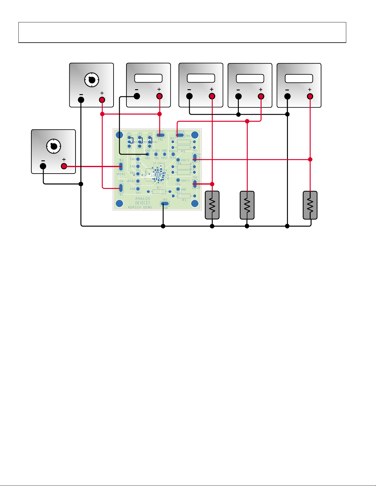
OUTPUT VOLTAGE MEASUREMENTS
VOLTMETER
1.99711
VOLTMETER VOLTMETER
1.99711 1.99711
VOLTAGE SOURCE
VOLTAGE SOURCE
VOLTMETER
1.99711
Figure 3. Output Voltage Measurement Setup
Figure 3 shows how the evaluation board can be connected to a
voltage source and voltmeters for basic output voltage accuracy
measurements. A resistor can be used as the load for the regulator. Ensure that the resistor has a power rating adequate to handle
the power expected to be dissipated across it. An electronic load
can be used as an alternative. In addition, ensure that the voltage
source can supply enough current for the expected load levels.
Follow these steps to connect to a voltage source and voltmeters:
1. Insert R1, R2, R3, R4, R5, and R6 to set voltages for an
ADP323. If an ADP322 is used, short R1, R3, and R5
to connect the output voltages to the feedback input for
each LDO.
2. Insert Jumpers JP1, JP2, and JP3 for automatic startup.
3. Connect the negative terminal (−) of the voltage sources to
one of the GND pads on the evaluation board.
4. Connect the positive terminal (+) of the main voltage
source to the VIN and VIN3 pads of the evaluation board.
5. Connect the positive terminal (+) of the bias voltage source
to the VBIAS pad of the evaluation board. Set the bias
voltage supply to a voltage from 2.5 V to 5.5 V.
6. Connect a load between VOUT1, VOUT2, and/or VOUT3
and one of the GND pads.
LOAD
LOAD LOAD
09299-003
7. Connect the negative terminal (−) of the voltmeters to one
of the GND pads.
8. Connect the positive terminal (+) of the voltmeters to
VOUT1, VOUT2, and/or VOUT3 and VIN/VIN3.
The voltage sources can now be turned on.
LINE REGULATION MEASUREMENTS
For line regulation measurements, the regulator’s outputs are
monitored while its input is varied. For good line regulation,
the outputs must change as little as possible with varying input
levels. To ensure that the device is not in dropout mode during
this measurement, V
(or 1.8 V, whichever is greater) and V
highest of the three output voltages. For example, for an ADP322/
ADP323 with a fixed 1.8 V output, V
2.3 V and 5.5 V. This measurement can be repeated under different
load conditions. Figure 4 shows the typical line regulation performance of the ADP322/ADP323 with a fixed 1.8 V output.
must be varied between V
IN
, where V
INMAX
must be varied between
IN
OUTNOM
OUTNOM
+ 0.5 V
is the
Rev. 0 | Page 4 of 12
Page 5

Evaluation Board User Guide UG-186
(V)
V
OUT
1.820
1.815
1.810
1.805
1.800
LOAD = 1mA
LOAD = 5mA
LOAD = 10mA
LOAD = 50mA
LOAD = 100mA
LOAD = 200mA
2.12.52.93.33.74.14.54.95.3
(V)
V
IN
9299-008
Figure 4. Output Voltage vs. Input Voltage
LOAD REGULATION MEASUREMENTS
For load regulation measurements, the regulator’s outputs are
monitored while the loads are varied. For good load regulation,
the outputs must change as little as possible with varying load.
The input voltage must be held constant during this measurement. The load currents can be varied from 0 mA to 200 mA
per output. Figure 5 shows the typical load regulation performance of a single 1.8 V output of the ADP322/ADP323 for an
input voltage of 2.3 V to 5.5 V.
1.820
1.815
DROPOUT VOLTAGE MEASUREMENTS
Dropout voltage can be measured using the configuration
shown in Figure 3. Dropout voltage is defined as the input-tooutput voltage differential when the input voltage is set to the
nominal output voltage. This applies only to output voltages
above 1.8 V. Dropout voltage increases with larger loads.
For more accurate measurements, an additional voltmeter can
be used to monitor the input voltage across the input capacitor.
The input supply voltage may need to be adjusted to account
for IR drops, especially if large load currents are used. Figure 6
shows the typical curve of the dropout voltage measurement
with different load currents.
100
90
80
70
60
50
40
30
DROPOUT VOLTAGE (mV)
20
10
0
1 10 100 1000
I
(mA)
LOAD
Figure 6. Dropout Voltage vs. Load Current, V
OUT
= 3.3 V
09299-022
(V)
1.810
OUT
V
1.805
1.800
1 10 100 1000
(mA)
I
LOAD
9299-007
Figure 5. Output Voltage vs. Load Current
Rev. 0 | Page 5 of 12
Page 6

UG-186 Evaluation Board User Guide
GROUND AND BIAS CURRENT MEASUREMENTS
AMMETER
VOLTAG E S OURCE
VOLTAGE SOURCE
VOLTMETER
1.99711
VOLTMETER
1.99711
LOAD LOAD LOAD
VOLTMETER
1.99711
AMMETER
0.00112
Figure 7. Ground and Bias Current Measurements Setup
Figure 7 shows how the evaluation board can be connected
to a voltage source and ammeters for ground and bias current
measurements. A resistor can be used as the load for the regulator. Ensure that the resistor has a power rating adequate to
handle the power expected to be dissipated across it. An electronic
load can be used as an alternative. Ensure that the voltage source
can supply enough current for the expected load levels.
Use the following steps to connect to a voltage source and
ammeters:
1. Insert R1, R2, R3, R4, R5, and R6 to set voltages for an
ADP323. If an ADP322 is used, short R1, R3, and R5
to connect the output voltages to the feedback input for
each LDO.
2. Insert Jumpers JP1, JP2, and JP3 for automatic startup.
3. Connect the positive terminal (+) of the main voltage
source to the VIN and VIN3 pads of the evaluation board.
4. Connect the negative terminal (−) of an ammeter to the
VBIAS pad of the evaluation board.
5. Connect the positive terminal (+) of the bias voltage source
to the positive terminal (+) of the ammeter connected to
the VBIAS pad. Set the bias voltage supply to a voltage
between 2.5 V and 5.5 V.
Rev. 0 | Page 6 of 12
09299-107
6. Connect the positive terminal (+) of the other ammeter to
one of the GND pads of the evaluation board.
7. Connect the negative terminal (−) of the ammeter con-
nected to GND to the negative (−) terminal of the main
voltage source.
8. Connect a load between VOUT1, VOUT2, and/or VOUT3
and the negative (−) terminal of the main voltage source.
The voltage sources can now be turned on.
GROUND CURRENT MEASUREMENT
Ground current measurements can determine how much current
the internal circuits of the regulator consume while the circuits
perform the regulation function. To be efficient, the regulator
must consume as little current as possible. Typically, the regulator
uses the maximum current when supplying its largest load level
(200 mA per output). Figure 8 shows the typical ground current
consumption for various load levels as a function of the input
voltage for all three outputs set to 1.2 V and loaded equally.
The ground current for the ADP323 also includes the current
through the output voltage setting dividers, R1 and R2, R3 and
R4, and R5 and R6.
Page 7

Evaluation Board User Guide UG-186
When the device is disabled (EN1, EN2, and EN3 = GND),
ground current drops to less than 1 μA.
300
250
200
150
100
GROUND CURRENT (µ A)
LOAD = 1mA
LOAD = 5mA
50
LOAD = 10mA
LOAD = 50mA
LOAD = 100mA
LOAD = 200mA
0
1.7 2.1 2.5 2.9 3.3 3.7 4.1 4.5 4.9 5.3
(V)
V
IN
9299-017
Figure 8. Ground Current vs. Input Voltage,
All Outputs Loaded Equally, ADP322
BIAS CURRENT MEASUREMENT
Bias current measurements can determine how much current
the regulator’s internal bias circuits consume while the circuits
perform the regulation function. The bias current typically does
not vary much with the load current or input voltage. Figure 8
shows the typical bias current consumption for various load
levels at a bias voltage of 4 V for all three outputs loaded equally.
100
90
80
70
60
50
40
BIAS CURRENT (µ A)
30
20
10
0
1 10 100 1000
I
(mA)
LOAD
Figure 9. Bias Current vs. Load Current, All Outputs Loaded Equally, ADP322
9299-019
Rev. 0 | Page 7 of 12
Page 8

UG-186 Evaluation Board User Guide
PRINTED CIRCUIT BOARD LAYOUT CONSIDERATIONS
Heat dissipation from the package can be improved by
increasing the amount of copper attached to the pins of
the ADP322/ADP323.
Place the input capacitor as close as possible to the VIN (VIN1/
VIN2), VIN3, VBIAS, and GND pins. Place the output capacitors as close as possible to the VOUT1, VOUT2, VOUT3, and
GND pins. Use 0402 or 0603 size capacitors and resistors to
achieve the smallest possible footprint solution on boards where
space is limited.
Figure 11. Typical Board Layout, Bottom Side
09299-011
9299-010
Figure 10. Typical Board Layout, Top Side
Rev. 0 | Page 8 of 12
Page 9

Evaluation Board User Guide UG-186
ORDERING INFORMATION
BILL OF MATERIALS
Table 2.
Qty Reference Designator Description Manufacturer/Vendor Vendor Part No.
6 C1, C2, C3, C4, C5, C6 Capacitor, MLCC, 1.0 μF, 10 V, 0402, X5R Murata or equivalent GRM155R61A105KE15
3 JP1, JP2, JP3 Header, single, STR, 3 pins Sullins Connector Solutions PEC03SAAN
6 R1, R2, R3, R4, R5, R6 Resistor, 1%, 0603 case Vishay CRCW0603xxxxF
1 U1 IC, LDO regulator Analog Devices, Inc. ADP322/ADP323
RELATED LINKS
Resource Description
ADP322 Product Page, ADP322 Fixed Output, Triple, 200 mA, Low Noise, High PSRR Voltage Regulator
ADP323 Product Page, ADP323 Adjustable Output, Triple, 200 mA, Low Noise, High PSRR Voltage Regulator
Rev. 0 | Page 9 of 12
Page 10

UG-186 Evaluation Board User Guide
NOTES
Rev. 0 | Page 10 of 12
Page 11

Evaluation Board User Guide UG-186
NOTES
Rev. 0 | Page 11 of 12
Page 12

UG-186 Evaluation Board User Guide
NOTES
ESD Caution
ESD (electrostatic discharge) sensitive device. Charged devices and circuit boards can discharge without detection. Although this product features patented or proprietary protection
circuitry, damage may occur on devices subjected to high energy ESD. Therefore, proper ESD precautions should be taken to avoid performance degradation or loss of functionality.
Legal Terms and Conditions
By using the evaluation board discussed herein (together with any tools, components documentation or support materials, the “Evaluation Board”), you are agreeing to be bound by the terms and conditions
set forth below (“Agreement”) unless you have purchased the Evaluation Board, in which case the Analog Devices Standard Terms and Conditions of Sale shall govern. Do not use the Evaluation Board until you
have read and agreed to the Agreement. Your use of the Evaluation Board shall signify your acceptance of the Agreement. This Agreement is made by and between you (“Customer”) and Analog Devices, Inc.
(“ADI”), with its principal place of business at One Technology Way, Norwood, MA 02062, USA. Subject to the terms and conditions of the Agreement, ADI hereby grants to Customer a free, limited, personal,
temporary, non-exclusive, non-sublicensable, non-transferable license to use the Evaluation Board FOR EVALUATION PURPOSES ONLY. Customer understands and agrees that the Evaluation Board is provided
for the sole and exclusive purpose referenced above, and agrees not to use the Evaluation Board for any other purpose. Furthermore, the license granted is expressly made subject to the following additional
limitations: Customer shall not (i) rent, lease, display, sell, transfer, assign, sublicense, or distribute the Evaluation Board; and (ii) permit any Third Party to access the Evaluation Board. As used herein, the term
“Third Party” includes any entity other than ADI, Customer, their employees, affiliates and in-house consultants. The Evaluation Board is NOT sold to Customer; all rights not expressly granted herein, including
ownership of the Evaluation Board, are reserved by ADI. CONFIDENTIALITY. This Agreement and the Evaluation Board shall all be considered the confidential and proprietary information of ADI. Customer may
not disclose or transfer any portion of the Evaluation Board to any other party for any reason. Upon discontinuation of use of the Evaluation Board or termination of this Agreement, Customer agrees to
promptly return the Evaluation Board to ADI. ADDITIONAL RESTRICTIONS. Customer may not disassemble, decompile or reverse engineer chips on the Evaluation Board. Customer shall inform ADI of any
occurred damages or any modifications or alterations it makes to the Evaluation Board, including but not limited to soldering or any other activity that affects the material content of the Evaluation Board.
Modifications to the Evaluation Board must comply with applicable law, including but not limited to the RoHS Directive. TERMINATION. ADI may terminate this Agreement at any time upon giving written notice
to Customer. Customer agrees to return to ADI the Evaluation Board at that time. LIMITATION OF LIABILITY. THE EVALUATION BOARD PROVIDED HEREUNDER IS PROVIDED “AS IS” AND ADI MAKES NO
WARRANTIES OR REPRESENTATIONS OF ANY KIND WITH RESPECT TO IT. ADI SPECIFICALLY DISCLAIMS ANY REPRESENTATIONS, ENDORSEMENTS, GUARANTEES, OR WARRANTIES, EXPRESS OR IMPLIED, RELATED
TO THE EVALUATION BOARD INCLUDING, BUT NOT LIMITED TO, THE IMPLIED WARRANTY OF MERCHANTABILITY, TITLE, FITNESS FOR A PARTICULAR PURPOSE OR NONINFRINGEMENT OF INTELLECTUAL
PROPERTY RIGHTS. IN NO EVENT WILL ADI AND ITS LICENSORS BE LIABLE FOR ANY INCIDENTAL, SPECIAL, INDIRECT, OR CONSEQUENTIAL DAMAGES RESULTING FROM CUSTOMER’S POSSESSION OR USE OF
THE EVALUATION BOARD, INCLUDING BUT NOT LIMITED TO LOST PROFITS, DELAY COSTS, LABOR COSTS OR LOSS OF GOODWILL. ADI’S TOTAL LIABILITY FROM ANY AND ALL CAUSES SHALL BE LIMITED TO THE
AMOUNT OF ONE HUNDRED US DOLLARS ($100.00). EXPORT. Customer agrees that it will not directly or indirectly export the Evaluation Board to another country, and that it will comply with all applicable
United States federal laws and regulations relating to exports. GOVERNING LAW. This Agreement shall be governed by and construed in accordance with the substantive laws of the Commonwealth of
Massachusetts (excluding conflict of law rules). Any legal action regarding this Agreement will be heard in the state or federal courts having jurisdiction in Suffolk County, Massachusetts, and Customer hereby
submits to the pers onal jurisdiction and venu e of such courts. The United Nations Conventi on on Contracts for the Internation al Sale of Goods shall not apply to this Agreement and is expressly disclaimed.
©2010 Analog Devices, Inc. All rights reserved. Trademarks and
registered trademarks are the property of their respective owners.
UG09299-0-10/10(0)
Rev. 0 | Page 12 of 12
 Loading...