

Page 1
Hardware User Guide
UG-180
One Technology Way • P. O . Box 9106 • Norwood, MA 02062-9106, U.S.A. • Tel : 781.329.4700 • Fax : 781.461.3113 • www.analog.com
Advantiv ADV7611 HDMI Receiver Functionality and Features
SCOPE
This user guide provides a detailed description of the Advantiv™ ADV7611 HDMI® receiver functionality and features.
DISCLAIMER
Information furnished by Analog Devices, Inc., is believed to be accurate and reliable. However, no responsibility is assumed by Analog
Devices for its use, nor any infringements of patents or other rights of third parties that may result from its use.
Specifications are subject to change without notice. No license is granted by implication or otherwise under any patent or patent rights of
Analog Devices. Trademarks and registered trademarks are the property of their respective owners.
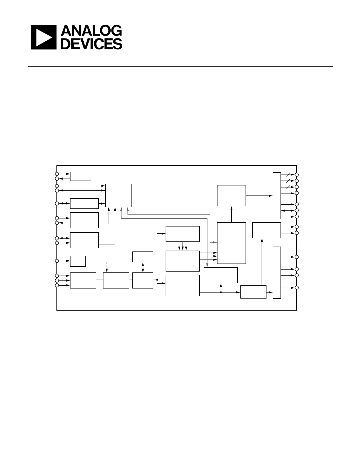
FUNCTIONAL BLOCK DIAGRAM
XTALP
XTALN
SCL
SDA
CEC
RXA_5V
HPA_A/INT2*
DDCA_SDA
DDCA_SCL
RXA_C±
RXA_0±
RXA_1±
RXA_2±
DPLL
CONTROL
INTERFACE
2
I
CEC
CONTRO LLER
5V DETECT
AND HPD
CONTRO LLER
EDID
REPEATER
CONTRO LLER
PLL
EQUALIZER EQUALIZE R
C
CONTROL
AND DATA
HDCP
EEPROM
HDCP
ENGINE
HDMI
PROCESSOR
DATA
PREPROCESSOR
AND COLOR
SPACE
CONVERSION
PACKET
PROCESSOR
BACKEND
COLOR SPACE
CONVERSION
COMPONENT
PROCESSOR
A
B
C
PACKET/
INFOFRAME
MEMORY
INTERRUPT
CONTRO LLER
(INT1, INT2)
MUTE
AUDIO
PROCESSOR
ADV7611
12
12
12
AUDIO OUTPUT FORMATTER OUTPUT FORMATTER
P0 TO P7
P8 TO P15
P16 TO P23
LLC
HS
VS/FIELD/ALSB
DE
INT1
INT2*
AP
LRCLK
SCLK/INT2*
MCLK/INT2*
*INT2 CAN BE ONLY OUTPUT ON ONE OF THE PINS: SCLK/INT2, MCLK/INT2, OR HPA_A/INT2.
Figure 1.
PLEASE SEE THE LAST PAGE FOR AN IMPORTANT
WARNING AND LEGAL TERMS AND CONDITIONS.
Rev. A | Page 1 of 184
09238-001
Page 2

UG-180 Hardware User Guide
TABLE OF CONTENTS
Scope .................................................................................................. 1
Disclaimer.......................................................................................... 1
Functional Block Diagram .............................................................. 1
Revision History ............................................................................... 5
Using the ADV7611 Hardware User Guide .................................. 6
Number Notations........................................................................ 6
Register Access Conventions ...................................................... 6
Acronyms and Abbreviations ..................................................... 6
Field Function Descriptions........................................................ 8
Example Field Function Description..................................... 8
References...................................................................................... 8
Introduction to the ADV7611 ........................................................ 9
HDMI Receiver............................................................................. 9
Component Processor ................................................................. 9
Main Features of ADV7611 ........................................................ 9
HDMI Receiver......................................................................... 9
Component Video Processing ................................................ 9
Video Output Formats........................................................... 10
Additional Features ................................................................ 10
Pin Configuration and Function Descriptions....................... 11
Global Control Registers ............................................................... 13
ADV7611 Revision Identification ............................................ 13
Power-Down Controls............................................................... 13
Primary Power-Down Controls ........................................... 13
Secondary Power-Down Controls ....................................... 13
Power-Down Modes .............................................................. 14
Global Pin Control..................................................................... 15
Reset Pin .................................................................................. 15
Reset Controls......................................................................... 15
Tristate Output Drivers ......................................................... 15
Tristate LLC Driver ................................................................16
Tristate Synchronization Output Drivers............................16
Tristate Audio Output Drivers..............................................16
Drive Strength Selection........................................................ 17
Output Synchronization Selection ....................................... 17
Output Synchronization Signals Polarity............................18
Digital Synthesizer Controls.................................................19
Crystal Frequency Selection ................................................. 19
Primary Mode and Video Standard............................................. 20
Primary Mode and Video Standard Controls......................... 20
V_FREQ .................................................................................. 22
HDMI Decimation Modes........................................................ 22
Primary Mode and Video Standard Configuration for
HDMI Free Run.......................................................................... 22
Recommended Settings for HDMI Inputs.............................. 23
Pixel Port Configuration ............................................................... 25
Pixel Port Output Modes........................................................... 25
Bus Rotation and Reordering Controls............................... 25
Pixel Data and Synchronization Signals Control............... 25
LLC Controls............................................................................... 26
DLL on LLC Clock Path............................................................ 26
Adjusting DLL Phase in All Modes ..................................... 26
DLL Settings for 656, 8-/10-/12-Bit Modes........................ 27
HDMI Receiver............................................................................... 28
+5 V Cable Detect ...................................................................... 28
Hot Plug Assert........................................................................... 29
E-EDID/Repeater Controller.................................................... 31
E-EDID Data Configuration..................................................... 31
Notes........................................................................................ 32
E-EDID Support for Power-Down Modes ......................... 32
Transitioning of Power Modes ................................................. 32
Structure of Internal E-EDID................................................... 32
Notes........................................................................................ 33
TMDS Equalization ................................................................... 33
Port Selection.............................................................................. 33
TMDS Clock Activity Detection .............................................. 33
Important ................................................................................ 34
Clock and Data Termination Control ................................. 34
HDMI/DVI Status Bits .............................................................. 34
Video 3D Detection ................................................................... 34
TMDS Measurement.................................................................. 35
TMDS Measurement after TMDS PLL ............................... 35
Deep Color Mode Support........................................................ 36
Notes........................................................................................ 36
Video FIFO.................................................................................. 36
Pixel Repetition .......................................................................... 38
HDCP Support ........................................................................... 39
HDCP Decryption Engine.................................................... 39
Internal HDCP Key OTP ROM........................................... 40
HDCP Keys Access Flags...................................................... 40
Rev. A | Page 2 of 184
Page 3

Hardware User Guide UG-180
HDCP Ri Expired ...................................................................42
HDMI Synchronization Parameters.........................................43
Notes.........................................................................................43
Horizontal Filter and Measurements ...................................43
Primary Port Horizontal Filter Measurements...................43
Horizontal Filter Locking Mechanism.................................45
Vertical Filters and Measurements .......................................45
Primary Port Vertical Filter Measurements ........................45
Vertical Filter Locking Mechanism ......................................48
Important.................................................................................48
Audio DPLL.............................................................................49
Locking Mechanism ...............................................................49
ACR Parameters Loading Method .......................................49
Audio DPLL Coast Feature....................................................49
Audio FIFO..................................................................................49
Audio Packet Type Flags ............................................................51
Notes.........................................................................................52
Audio Output Interface ..............................................................53
I2S/SPDIF Audio Interface and Output Controls...............54
Notes.........................................................................................55
MCLKOUT Setting.....................................................................57
Audio Channel Mode.................................................................58
Audio Muting ..............................................................................58
Delay Line Control .................................................................58
Audio Mute Configuration....................................................59
Internal Mute Status ...............................................................61
AV Mute Status........................................................................61
Audio Mute Signal ..................................................................61
Audio Stream with Incorrect Parity Error...........................62
Audio Clock Regeneration Parameters ....................................62
ACR Parameters Readbacks ..................................................62
Monitoring ACR Parameters.................................................62
Channel Status.............................................................................63
Validity Status Flag..................................................................63
General Control and Mode Information .............................64
Category Code.........................................................................65
Source Number and Channel Number ................................65
Sampling and Frequency Accuracy ......................................66
Word Length............................................................................66
Channel Status Copyright Value Assertion .........................67
Monitoring Change of Audio Sampling Frequency ...........67
Packets and InfoFrames Registers ............................................67
InfoFrames Registers..............................................................67
InfoFrame Collection Mode..................................................68
InfoFrame Checksum Error Flags........................................68
AVI InfoFrame Registers .......................................................69
Audio InfoFrame Registers....................................................70
SPD InfoFrame Registers.......................................................71
MPEG Source InfoFrame Registers......................................72
Vendor Specific InfoFrame Registers...................................73
Packet Registers...........................................................................74
ACP Packet Registers .............................................................74
ISRC Packet Registers.............................................................75
Gamut Metadata Packets .......................................................77
Customizing Packet/InfoFrame Storage Registers .................78
Repeater Support.........................................................................79
Repeater Routines Performed by the EDID/Repeater
Controller.................................................................................79
Repeater Actions Required by External Controller ...........80
HDCP Registers Available in Repeater Map.......................81
Interface to DPP Section............................................................86
Notes.........................................................................................87
Pass Through Mode....................................................................87
4:2:2 Pass Through..................................................................87
4:4:4 Pass Through..................................................................87
Color Space Information Sent to the DPP and
CP Sections ..................................................................................88
Status Registers............................................................................88
HDMI Section Reset Strategy ...................................................91
HDMI Packet Detection Flag Reset .........................................91
Data Preprocessor and Color Space Conversion and Color
Controls............................................................................................92
Color Space Conversion Matrix................................................92
CP CSC Selection....................................................................92
Selecting Auto or Manual CP CSC Conversion Mode......93
Auto Color Space Conversion Matrix..................................93
HDMI Automatic CSC Operation........................................95
Manual Color Space Conversion Matrix .............................97
CSC in Pass-Through Mode................................................101
Color Controls...........................................................................101
Component Processor..................................................................103
Introduction to the Component Processor ...........................103
Clamp Operation ......................................................................103
Rev. A | Page 3 of 184
Page 4

UG-180 Hardware User Guide
CP Gain Operation................................................................... 105
Features of Manual Gain Control ...................................... 105
Features of Automatic Gain Control .................................105
Manual Gain and Automatic Gain Control Selection.....105
Manual Gain Control...........................................................106
Manual Gain Filter Mode....................................................108
Other Gain Controls............................................................108
CP Offset Block......................................................................... 109
Notes ......................................................................................109
AV Code Block.......................................................................... 110
CP Data Path for HDMI Modes ............................................. 112
Pregain Block ........................................................................ 112
Sync Processed by CP Section ................................................115
Sync Routing from HDMI Section .................................... 115
Standard Detection and Identification.............................. 115
Detailed Mechanism of STDI Block Horizontal/Vertical
Lock Mechanism ..................................................................118
CP Output Synchronization Signal Positioning................... 122
CP Synchronization Signals ................................................ 124
HSync Timing Controls ...................................................... 124
VSync Timing Controls.......................................................126
DE Timing Controls ............................................................ 128
FIELD Timing Controls......................................................129
HCOUNT Timing Control................................................. 133
CP HDMI Controls.................................................................. 134
Free Run Mode .........................................................................134
Free Run Mode Thresholds.................................................134
Free Run Feature in HDMI Mode...................................... 136
Free Run Default Color Output.......................................... 137
CP Status.................................................................................... 138
CP_REG_FF.......................................................................... 138
CP Core Bypassing.................................................................... 138
Consumer Electronics Control................................................... 139
Main Controls........................................................................... 139
CEC Transmit Section ............................................................. 140
CEC Receive Section................................................................ 142
Logical Address Configuration ..........................................142
Receive Buffers...................................................................... 143
CEC Message Reception Overview.................................... 146
Antiglitch Filter Module .......................................................... 147
Typical Operation Flow ...........................................................148
Initializing CEC Module..................................................... 148
Using CEC Module as Initiator.......................................... 149
Using CEC Module as Follower .........................................150
Low Power CEC Message Monitoring................................... 151
Interrupts....................................................................................... 153
Interrupt Architecture Overview........................................... 153
Interrupt Pins............................................................................ 156
Notes...................................................................................... 156
Interrupt Duration............................................................... 157
Interrupt Drive Level........................................................... 157
Interrupt Manual Assertion................................................ 157
Multiple Interrupt Events.................................................... 158
Description of Interrupt Bits .................................................. 159
General Operation ...............................................................159
HDMI Video Mode.............................................................. 159
CEC........................................................................................ 159
HDMI Only Mode ...............................................................159
Additional Explanations.......................................................... 160
STDI_DATA_VALID_RAW............................................... 160
CP_LOCK, CP_UNLOCK ................................................. 161
HDMI Interrupts Validity Checking Process ................... 161
Storing Masked Interrupts .................................................. 163
Register Access and Serial Ports Description ........................... 174
Main I2C Port............................................................................ 174
Register Access .....................................................................174
IO I2C Map Address............................................................. 174
Addresses of Other Maps.................................................... 175
Protocol for Main I2C Port.................................................. 176
DDC Ports................................................................................. 177
I2C Protocols for Access to the Internal EDID................. 177
I2C Protocols for Access to HDCP Registers.................... 177
DDC Port A .......................................................................... 177
Appendix A ................................................................................... 178
PCB Layout Recommendations .............................................178
Power Supply Bypassing.......................................................... 178
Example of a Current Loop................................................. 178
Digital Outputs (Data and Clocks)........................................ 178
Digital Inputs ............................................................................ 179
XTAL and Load Cap Value Selection .................................... 179
Example................................................................................. 179
Rev. A | Page 4 of 184
Page 5

Hardware User Guide UG-180
Appendix B .................................................................................... 180
Recommended Unused Pin Configurations ........................ 180
REVISION HISTORY
12/11—Rev. 0 to Rev. A
Change to Video Output Formats Section ................................... 10
Changes to RD_INFO[15:0] Table in ADV7611 Revision
Identification Section ...................................................................... 13
Change to XTAL_FREQ_SEL[1:0] Table in Crystal
Frequency Selection Section .......................................................... 19
Changes to Table 7 .......................................................................... 23
Added Endnote to OP_FORMAT_SEL[7:0] Table in Pixel
Port Output Modes Section ........................................................... 25
Added LLC_DLL_DOUBLE to DLL on LLC C
ction .............................................................................................. 26
Se
lock Path
Appendix C .................................................................................... 182
Pixel Output Formats ............................................................... 182
Added DLL Settings for 656, 8-/10-/12-Bit Modes Section ...... 27
Changes to Audio Mute Signal Section ........................................ 61
Added 1001 to CS_DATA[27:24] Table in Sampling and
Frequency Accuracy Section ......................................................... 66
Changes to Check the Value of Each Coefficient Section ....... 100
Changes to CP_HUE[7:0], Addr 44 (CP), Address 0x3D[7:0]
in Color Controls Section; Changes to CP_HUE[7:0] Table ..... 102
Changes to INT2_POL Table in Interrupt Drive Level Section ... 157
Added Endnote to Table 71 ......................................................... 182
10/10—Revision 0: Initial Version
Rev. A | Page 5 of 184
Page 6

UG-180 Hardware User Guide
USING THE ADV7611 HARDWARE USER GUIDE
NUMBER NOTATIONS
Table 1.
Notation Description
Bit N Bits are numbered in little endian format, that is, the least significant bit of a number is referred to as Bit 0.
V[X:Y] Bit field representation covering Bit X to Bit Y of a value or a field (V).
0xNN Hexadecimal (base-16) numbers are preceded by the prefix ‘0x’.
0bNN Binary (base-2) numbers are preceded by the prefix ‘0b’.
NN Decimal (base-10) are represented using no additional prefixes or suffixes.
REGISTER ACCESS CONVENTIONS
Table 2.
Mode Description
R/W Memory location has read and write access.
R Memory location is read access only. A read always returns 0 unless otherwise specified.
W Memory location is write access only.
ACRONYMS AND ABBREVIATIONS
Table 3.
Acronym/Abbreviation Description
ACP Audio content protection.
AGC Automatic gain control.
Ainfo HDCP register. Refer to digital content protection documentation in the References section.
AKSV
An 64-bit pseudo-random value generated by HDCP cipher function of Device A.
AP Audio output pin.
AVI Auxiliary video information.
BCAPS HDCP register. Refer to digital content protection documentation in the References section.
BKSV HDCP receiver key selection vector. Refer to digital content protection documentation in the References section.
CP Component processor.
CSC Color space converter/conversion.
DDR Double data rate.
DE Data enable.
DLL Delay locked loop.
DPP Data preprocessor.
DVI Digital visual interface.
EAV End of active video.
EMC Electromagnetic compatibility.
EQ Equalizer.
HD High definition.
HDCP High bandwidth digital content protection.
HDMI High bandwidth multimedia interface.
HDTV High definition television.
HPA Hot plug assert.
HPD Hot plug detect.
HSync Horizontal synchronization.
IC Integrated circuit.
ISRC International standard recording code.
I2S Inter IC sound.
HDCP transmitter key selection vector. Refer to digital content protection documentation in the References
section.
Rev. A | Page 6 of 184
Page 7

Hardware User Guide UG-180
Acronym/Abbreviation Description
I2C Inter integrated circuit.
KSV Key selection vector.
LLC Line locked clock.
LSB Least significant bit.
L-PCM Linear pulse coded modulated.
Mbps Megabit per second.
MPEG Moving picture expert group.
ms Millisecond.
MSB Most significant bit.
NC No connect.
OTP One-time programmable.
Pj’
Ri’ HDCP link verification response. Refer to digital content protection documentation in the References section.
Rx Receiver.
SAV Start of active video.
SDR Single data rate.
SHA-1 Refer to HDCP documentation.
SMPTE Society of Motion Picture and Television Engineers.
SOG Sync on green.
SOY Sync on Y.
SPA Source physical address.
SPD Source production descriptor.
STDI Standard detection and identification.
TDM Time division multiplexed.
TMDS Transition minimized differential signaling.
Tx Transmitter.
VBI Video blanking interval.
VSync Vertical synchronization.
XTAL Crystal oscillator.
HDCP enhanced link verification response. Refer to digital content protection documentation in the References
section.
Rev. A | Page 7 of 184
Page 8

UG-180 Hardware User Guide
FIELD FUNCTION DESCRIPTIONS
Throughout this user guide, a series of function tables are provided. The function of a field is described in a table preceded by the bit
name, a short function description, the I
The detailed description consists of:
• For a readable field, the values the field can take
• For a writable field, the values the field can be set to
Example Field Function Description
This section provides an example of a field function table followed by a description of each part of the table.
PRIM_MODE[3:0], IO Map, Address 0x01[3:0].
A control to select the primary mode of operation of the decoder.
Function
PRIM_MODE[3:0] Description
0000 Reserved
0001 Reserved
0010 Reserved
0011 Reserved
0100 Reserved
0101 HDMI-Comp
0110 (default) HDMI-GR
0111 to 1111 Reserved
In this example
• The name of the field is PRIM_MODE and it is four bit long.
2
• Address 0x01 is the I
C location of the field in big endian format (MSB first, LSB last).
• The address is followed by a detailed description of the field.
2
C map, the register location within the I2C map, and a detailed description of the field.
• The first column of the table lists values the field can take or can be set to. These values are in binary format if not preceded by 0x or
in hexadecimal format if preceded by 0x.
• The second column describes the function of each field for each value the field can take or can be set to. Values are in binary format.
REFERENCES
CEA, CEA-861-D, A DTV Profile for Uncompressed High Speed Digital Interfaces, Revision D, July 18, 2006.
Digital Content Protection (DCP) LLC, High-Bandwidth Digital Content Protection System, Revision 1.4, July 8, 2009.
HDMI Licensing and LLC, High-Definition Multimedia Interface, Revision 1.4a, March 4, 2010.
ITU, ITU-R BT.656-4, Interface for Digital Component Video Signals in 525-Line and 625-Line Television Systems Operating
at the 4:2:2 Level of Recommendation ITU-R BT.601, February 1998.
Rev. A | Page 8 of 184
Page 9

Hardware User Guide UG-180
INTRODUCTION TO THE ADV7611
The ADV7611 is a high quality, single input, high definition multimedia interface (HDMI®) receiver. It incorporates an HDMI receiver
that supports all mandatory HDMI 1.4a 3D TV formats up to 1080 p60@8-bit. It integrates a CEC controller that supports the capability
discovery and control (CDC) feature.
The ADV7611 has an audio output port for the audio data extracted from the HDMI stream. The receiver has an advanced mute
controller that prevents audible extraneous noise in the audio output. Additionally, the ADV7611 can be set to output TDM I
allows four multiplexed I
2
S channels to be sent.
Fabricated in an advanced CMOS process, the ADV7611 is provided in a 10 mm × 10 mm, 64-pin surface-mount LQFP_EP, RoHScompliant package and is specified over the −40°C to +85°C temperature range.
HDMI RECEIVER
The ADV7611 HDMI receiver incorporates equalization of the HDMI data signals to compensate for the losses inherent in HDMI and
DVI cabling, especially at longer lengths and higher frequencies. The equalizer is highly effective and is capable of equalizing for long
cables to achieve robust receiver performance.
With the inclusion of high-bandwidth digital content protection (HDCP), displays can receive encrypted video content. The HDMI
interface of the ADV7611 allows a video receiver to authenticate, decrypt encoded data and renew that authentication during
transmission, as specified by the HDCP v1.4 protocol.
The ADV7611 offers an audio output port for audio data extraction from the HDMI stream. The receiver has an advanced mute
controller that prevents audible extraneous noise in the audio output. Additionally, the ADV7611 can be set to output time division
multiplexed (TDM) I
2
S, which allows four multiplexed I2S channels to be sent.
2
S, which
COMPONENT PROCESSOR
The component processor (CP) is located behind the HDMI receiver. It processes the video data received from the HDMI receiver. The
CP section provides color adjustment features, such as brightness, saturation, and hue. The color space conversion (CSC) matrix allows
the color space to be changed as required. The standard detection and identification (STDI) block allows the detection of video timings.
MAIN FEATURES OF ADV7611
HDMI Receiver
• HDMI 1.4a features supported
• 3D HDMI 1.4a video format support
• Full colorimetry, including sYCC601, Adobe RGB, Adobe YCC601, and xvYCC extended gamut color
• CEC 1.4-compatible
• HDCP v1.4-compliant receiver
• Supports all display resolutions up to UXGA 60 Hz 8-bit
• Supports stereo audio formats with a sampling frequency up to 192 kHz
• Supports multichannel audio with sampling frequency up to 48 kHz in TDM I
• Programmable front-end equalization for long cable lengths
• Audio mute for removing extraneous noise
• Programmable interrupt generator to detect HDMI packets
• Internal EDID support
• Repeater support
Component Video Processing
• An any-to-any 3 × 3 CSC matrix support YCrCb to RGB and RGB to YCrCb
• Provides color controls, such as saturation, brightness, hue, and contrast
• STDI block that enables format detection
• Free run output mode provides stable timing when no video input is present
2
S mode
Rev. A | Page 9 of 184
Page 10

UG-180 Hardware User Guide
Video Output Formats
• Double data rate (DDR) 8-/12-bit 4:2:2 YCrCb.
• DDR supported only up to 50 MHz (an equivalent to ata rate clocked with 100 MHz clock in SDR mode)
• Pseudo DDR (CCIR-656 type stream) 8-/12-bit 4:2:2 YCrCb for 525i, 625i, 525P, and 625P
• SDR 16-/24-bit 4:2:2 YCrCb for all standards
• SDR 24-bit 4:4:4 YCrCb/RGB for all HDMI standards
• DDR 24-bit 4:4:4 RGB
Additional Features
• HS, VS, FIELD, and DE output signals with programmable position, polarity, and width
• Numerous interrupt sources available for the INT1 and INT2 interrupt request output pins, available via one of the selected pins, that
is, SCLK/INT2, MCLK/INT2, or HPA_A/INT2
• Temperature range of −40°C to +85°C
• 10 mm × 10 mm, 64-pin LQFP_EP package
Rev. A | Page 10 of 184
Page 11
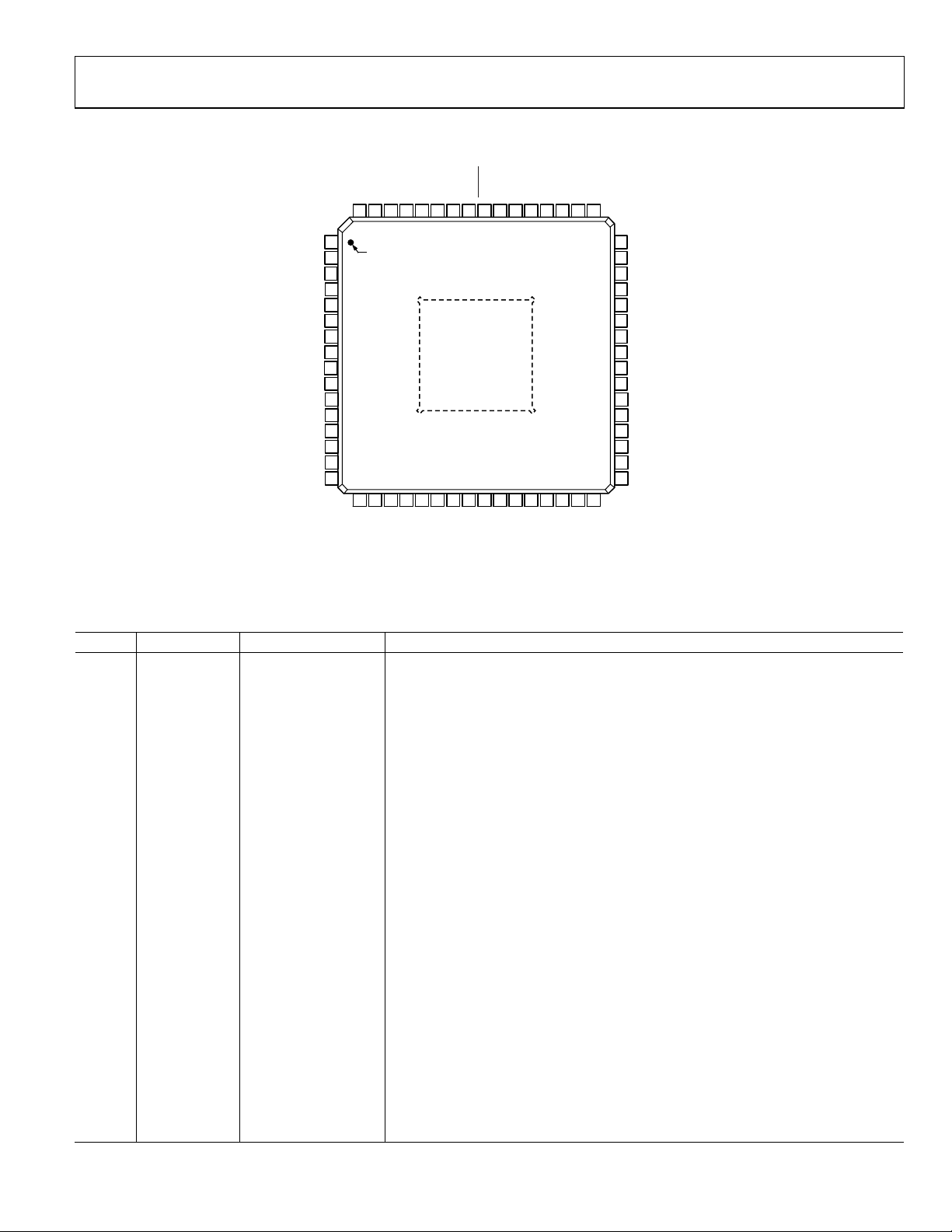
Hardware User Guide UG-180
A
A
PIN CONFIGURATION AND FUNCTION DESCRIPTIONS
RXA_5V63DDCA_SD
DDCA_SD
64
CEC60DVDD59XTALN58XTALP57PVDD56RESET55INT154SDA53SCL52DVDD51MCLK/INT250LRCLK49SCLK/INT2
62
61
CVDD
TVDD
RXA_0–
RXA_0+
TVDD
RXA_1–
RXA_1+
TVDD
RXA_2–
RXA_2+
CVDD
P23
P22
1
2
3
4
5
6
7
8
9
10
11
12
13
14
15
16
17
PIN 1
P2118P2019P1920P1821P1722P16
ADV7611
TOP VIEW
(Not to Scale)
23
24
25
LLC
DVDD
DVDDIO
26
P1527P1428P1329P12
HPA_A/INT2
RXA_C–
RXA_C+
NOTES
1. CONNECT EXP OSED PAD–PIN0 TO GROUND (BOTTOM) .
30
P11
48
AP
47
VS/FIELD/ALSB
46
HS
45
DE
44
DVDDIO
43
P0
42
P1
41
P2
40
DVDD
39
P3
38
P4
37
P5
36
P6
35
P7
34
DVDDIO
33
P8
31
32
P9
P10
09238-003
Figure 2. Pin Configuration
Table 4. Pin Function Descriptions
Pin No. Mnemonic Type Description
0 GND Ground Ground.
1 HPA_A/INT2 Miscellaneous digital
A dual function pin that can be configured to output Hot Plug Assert signal (for HDMI
Port A) or an Interrupt2 signal.
2 CVDD Power HDMI Analog Block Supply Voltage (1.8 V).
3 RXA_C− HDMI input Digital Input Clock Complement of Port A in the HDMI Interface.
4 RXA_C+ HDMI input Digital Input Clock True of Port A in the HDMI Interface.
5 TVDD Power Terminator Supply Voltage (3.3 V).
6 RXA_0− HDMI input Digital Input Channel 0 Complement of Port A in the HDMI Interface.
7 RXA_0+ HDMI input Digital Input Channel 0 True of Port A in the HDMI Interface.
8 TVDD Power Terminator Supply Voltage (3.3 V).
9 RXA_1− HDMI input Digital Input Channel 1 Complement of Port A in the HDMI Interface.
10 RXA_1+ HDMI input Digital Input Channel 1 True of Port A in the HDMI Interface.
11 TVDD Power Terminator Supply Voltage (3.3 V).
12 RXA_2− HDMI input Digital Input Channel 2 Complement of Port A in the HDMI Interface.
13 RXA_2+ HDMI input Digital Input Channel 2 True of Port A in the HDMI Interface.
14 CVDD Power HDMI Analog Block Supply Voltage (1.8 V).
15 P23 Digital video output Video Pixel Output Port.
16 P22 Digital video output Video Pixel Output Port.
17 P21 Digital video output Video Pixel Output Port.
18 P20 Digital video output Video Pixel Output Port.
19 P19 Digital video output Video Pixel Output Port.
20 P18 Digital video output Video Pixel Output Port.
21 P17 Digital video output Video Pixel Output Port.
22 P16 Digital video output Video Pixel Output Port.
23 DVDDIO Power Digital I/O Supply Voltage (3.3 V).
24 DVDD Power Digital Core Supply Voltage (1.8 V).
Rev. A | Page 11 of 184
Page 12

UG-180 Hardware User Guide
Pin No. Mnemonic Type Description
25 LLC Digital video output Line Locked Output Clock for the Pixel Data (Range is 13.5 MHz to 162.5 MHz).
26 P15 Digital video output Video Pixel Output Port.
27 P14 Digital video output Video Pixel Output Port.
28 P13 Digital video output Video Pixel Output Port.
29 P12 Digital video output Video Pixel Output Port.
30 P11 Digital video output Video Pixel Output Port.
31 P10 Digital video output Video Pixel Output Port.
32 P9 Digital video output Video Pixel Output Port.
33 P8 Digital video output Video Pixel Output Port.
34 DVDDIO Power Digital I/O Supply Voltage (3.3 V).
35 P7 Digital video output Video Pixel Output Port.
36 P6 Digital video output Video Pixel Output Port.
37 P5 Digital video output Video Pixel Output Port.
38 P4 Digital video output Video Pixel Output Port.
39 P3 Digital video output Video Pixel Output Port.
40 DVDD Power Digital Core Supply Voltage (1.8 V).
41 P2 Digital video output Video Pixel Output Port.
42 P1 Digital video output Video Pixel Output Port.
43 P0 Digital video output Video Pixel Output Port.
44 DVDDIO Power Digital I/O Supply Voltage (3.3 V).
45 DE Miscellaneous digital DE (data enable) is a signal that indicates active pixel data.
46 HS Digital video output HS is a horizontal synchronization output signal.
47 VS/FIELD/ALSB Digital input/output
48 AP Miscellaneous
49 SCLK/INT2 Miscellaneous digital
50 LRCLK Miscellaneous Audio Left/Right Clock.
51 MCLK/INT2 Miscellaneous
52 DVDD Power Digital Core Supply Voltage (1.8 V).
53 SCL Miscellaneous digital I2C Port Serial Clock Input. SCL is the clock line for the control port.
54 SDA Miscellaneous digital I2C Port Serial Data Input/Output Pin. SDA is the data line for the control port.
55 INT1 Miscellaneous digital
56
RESET
Miscellaneous digital
57 PVDD Power PLL Supply Voltage (1.8 V).
58 XTALP Miscellaneous analog
59 XTALN Miscellaneous analog Crystal Input. Input pin for 28.63636 MHz crystal.
60 DVDD Power Digital Core Supply Voltage (1.8 V).
61 CEC Digital input/output Consumer Electronic Control Channel.
62 DDCA_SCL HDMI input HDCP Slave Serial Clock Port A. DDCA_SCL is a 3.3 V input that is 5 V tolerant.
63 DDCA_SDA HDMI input HDCP Slave Serial Data Port A. DDCA_SDA is a 3.3 V input that is 5 V tolerant.
64 RXA_5V HDMI input 5 V Detect Pin for Port A in the HDMI Interface.
VS is a vertical synchronization output signal. FIELD is a field synchronization output
signal in all interlaced video modes. VS or FIELD can be configured for this pin. The
ALSB allows selection of the I
Audio Output Pin. Pin can be configured to output SPDIF Digital Audio Output (SPDIF)
or Time-Division-Multiplexed I
2
C address.
2
S.
A dual function pin that can be configured to output Audio Serial Clock or an
Interrupt2 signal.
A dual fuction pin that can be configured to output Audio Master Clock or an
Interrupt2 signal.
Interrupt. This pin can be active low or active high. When status bits change, this pin is
triggered. The events that trigger an interrupt are under user configuration.
System Reset Input. Active low. A minimum low reset pulse width of 5 ms is required
to reset the ADV7611 circuitry.
Input Pin for 28.63636 MHz Crystal or an External 1.8 V, 28.63636 MHz Clock Oscillator
Source to Clock the ADV7611.
Rev. A | Page 12 of 184
Page 13

Hardware User Guide UG-180
GLOBAL CONTROL REGISTERS
The register control bits described in this section deal with the general control of the chip, and the CP and the HDMI receiver sections of
the ADV7611.
ADV7611 REVISION IDENTIFICATION
RD_INFO[15:0], IO, Address 0xEA[7:0]; Address 0xEB[7:0] (Read Only)
Chip revision code.
Function
RD_INFO[15:0] Description
0x2041 = Final Silicon ADV7612 ADV7612
0x2051 = Final Silicon ADV7611 ADV7611
POWER-DOWN CONTROLS
Primary Power-Down Controls
POWER_DOWN is the main power-down control. It is the main control for power-down Mode 0 and Mode 1. See the Power-Down
Modes section for more details.
POWER_DOWN, IO, Address 0x0C[5]
A control to enable power-down mode. This is the main I
Function
POWER_DOWN Description
0 Chip operational
1 (default) Enables chip power down
Secondary Power-Down Controls
The following controls allow various sections of the ADV7611 to be powered down.
It is possible to stop the clock to the CP to reduce power for a power-sensitive application. The CP_PWRDN bit enables this power-save
mode. The HDMI block is not affected by this power-save mode. This allows the use of limited HDMI, STDI monitoring features while
reducing the power consumption. For full processing of the HDMI input, the CP core needs to be powered up.
CP_PWRDN, IO, Address 0x0C[2]
A power-down control for the CP core.
Function
CP_PWRDN Description
0 (default) Powers up clock to CP core.
1 Powers down clock to CP core. HDMI block not affected by this bit.
XTAL_PDN
XTAL_PDN allows the user to power down the XTAL clock in the following sections:
2
C power-down control.
• STDI blocks
• Free run synchronization generation block
2
C sequencer block, which is used for the configuration of the gain, clamp, and offset
• I
• CP and HDMI section
The XTAL clock is also provided to the HDCP engine, EDID, and the repeater controller within the HDMI receiver. The XTAL clock
within these sections is not affected by XTAL_PDN.
XTAL_PDN, IO, Address 0x0B[0]
A power-down control for the XTAL in the digital blocks.
Function
XTAL_PDN Description
0 (default) Powers up XTAL buffer to digital core
1 Powers down XTAL buffer to digital core
Rev. A | Page 13 of 184
Page 14

UG-180 Hardware User Guide
CORE_PDN
CORE_PDN allows the user to power down clocks, with the exception of the XTAL clock, in the following sections:
• CP block
• Digital section of the HDMI block
CORE_PDN, IO, Address 0x0B[1]
A power-down control for the DPP, CP core, and digital sections of the HDMI core.
Function
CORE_PDN Description
0 (default) Powers up CP and digital sections of HDMI block
1 Powers down CP and digital section of HDMI block
Power-Down Modes
The ADV7611 supports the following power-down modes:
• Power-Down Mode 0
• Power-Down Mode 1
Tabl e 5 shows the power-down and normal modes of ADV7611.
Table 5. Power-Down Modes
POWER_DOWN Bit CEC_POWER_UP Bit CEC EDID Power-Down Mode
0 0 Disabled Enabled Power-Down Mode 0
0 1 Enabled Enabled Power-Down Mode 1
1 0 Disabled Enabled1 Normal mode
1 1 Enabled Enabled1 Normal mode
1
Dependent on the values of EDID_X_ENABLE_CPU and EDID_X_ENABLE for the HDMI port (where X is A).
Power-Down Mode 0
In Power-Down Mode 0, selected sections and pads are kept active to provide EDID and +5 V antiglitch filter functionality.
In Power-Down Mode 0, the sections of the ADV7611 are disabled except for the following blocks:
• I2C slave section
• EDID/repeater controller
• EDID ring oscillator
The ring oscillator provides a clock to the EDID/repeater controller (refer to the E-EDID/Repeater Controller section) and the +5 V
power supply antiglitch filter. The clock output from the ring oscillator runs at approximately 50 MHz.
The following pads only are enabled in Power-Down Mode 0:
2
• I
C pads
• SDA
• SCL
• +5 V pads
• RXA_5V
• HPA_A
• DDC pads
• DDCA_SCL
• DDCA_SDA
• Reset pad
Power-Down Mode 0 is initiated through a software (I
RESET
2
C register) configuration.
Rev. A | Page 14 of 184
Page 15

Hardware User Guide UG-180
Entering Power-Down Mode 0 via Software
The ADV7611 can be put into Power-Down Mode 0 by setting POWER_DOWN to 1 (default value) and CEC_POWER_UP to 0. This
method allows an external processor to put the system in which the ADV7611 is integrated into standby mode. In this case, the CP and
HDMI cores of the ADV7611 are kept powered up from the main power (for example, ac power) and set in or out of power-down Mode 0
through the POWER_DOWN bit.
Power-Down Mode 1
Power-Down Mode 1 is enabled when the following conditions are met:
• POWER_DOWN bit is set to 1
• CEC section is enabled by setting CEC_POWER_UP to 1
Power-Down Mode 1 provides the same functionality as Power-Down Mode 0, with the addition of the following sections:
• XTAL clock
• CEC section
• Interrupt controller section
The following pads are enabled in Power-Down Mode 1:
• Same pads as enabled in Power-Down Mode 0
• CEC pad
• INT1 and INT2 interrupt pads
The internal EDID is also accessible through the DDC bus for Port A in Power-Down Mode 0 and Power-Down Mode 1.
GLOBAL PIN CONTROL
Reset Pin
The ADV7611 can be reset by a low reset pulse on the reset pin with a minimum width of 5 ms. It is recommended to wait 5 ms after the
low pulse before an I
Reset Controls
MAIN_RESET, IO, Address 0xFF[7] (Self-Clearing)
Main reset where I
Function
MAIN_RESET Description
0 (default) Normal operation
1 Applies main I2C reset
Tristate Output Drivers
PA D S _ P DN , IO, Address 0x0C[0]
A power-down control for pads of the digital output s. When enabled, the pads are tristated and the input path is disabled. This control
applies to the DE, HS, VS/FIELD/ALSB, INT1, and LLC pads and to the P0 to P23 pixel pads.
Function
PADS_PDN Description
0 (default) Powers up pads of digital output pins
1 Powers down pads of digital output pins
DDC_PWRDN[7:0], Addr 68 (HDMI), Address 0x73[7:0]
A power-down control for DDC pads.
Function
DDC_PWRDN[7:0] Description
0 (default) Powers up DDC pads
1 Powers down DDC pads
2
C write is performed to the ADV7611.
2
C registers are reset to their default values.
Rev. A | Page 15 of 184
Page 16

UG-180 Hardware User Guide
TRI_PIX
This bit allows the user to tristate the output driver of pixel outputs. Upon setting TRI_PIX, the pixel output P[23:0] is tristated.
TRI_PIX, IO, Address 0x15[1]
A control to tristate the pixel data on the pixel pins, P[23:0].
Function
TRI_PIX Description
0 Pixel bus active
1 (default) Tristates pixel bus
Tristate LLC Driver
TRI_LLC, IO, Address 0x15[2]
A control to tristate the output pixel clock on the LLC pin.
Function
TRI_LLC Description
0 LLC pin active
1 (default) Tristates LLC pin
Tristate Synchronization Output Drivers
The following output synchronization signals are tristated when TRI_SYNCS is set:
• VS/FIELD/ALSB
• HS
• DE
The drive strength controls for these signals are provided via the DR_STR_SYNC bits. The ADV7611 does not support tristating via a
dedicated pin.
TRI_SYNCS, IO, Address 0x15[3]
Synchronization output pins tristate control. The synchronization pins under this control are HS, VS/FIELD/ALSB, and DE.
Function
TRI_SYNCS Description
0 Sync output pins active
1 (default) Tristates sync output pins
Tristate Audio Output Drivers
TRI_AUDIO, IO Map, Address 0x15[4]
TRI_AUDIO allows the user to tristate the drivers of the following audio output signals:
• AP
• SCLK/INT2
• LRCLK
• MCLK/INT2
The drive strength for the output pins can be controlled by the DR_STR[1:0] bits. The ADV7611 does not support tristating via a
dedicated pin.
TRI_AUDIO, IO, Address 0x15[4]
A control to tristate the audio output interface pins (AP).
Function
TRI_AUDIO Description
0 Audio output pins active
1 (default) Tristates audio output pins
Rev. A | Page 16 of 184
Page 17

Hardware User Guide UG-180
Drive Strength Selection
DR_STR
It may be desirable to strengthen or weaken the drive strength of the output drivers for electromagnetic compatibility (EMC)
and crosstalk reasons. This section describes the controls to adjust the output drivers used by the CP and HDMI modes.
The drive strenth DR_STR_SYNC[1:0] bits allow the user to select the strength of the following synchronization signals:
• DE
• HS
• VS/FIELD
The DR_STR[1:0] drive strength bits affect output drivers for the following output pins:
• P[23:0]
• AP
• SCLK
• SDA
• SCL
The drive strength DR_STR_CLK[1:0] bits affect output driver for LLC line.
DR_STR[1:0], IO, Address 0x14[5:4]
A control to set the drive strength of the data output drivers.
Function
DR_STR[1:0] Description
00 Reserved
01 Medium low (2×)
10 (default) Medium high (3×)
11 High (4×)
DR_STR_CLK[1:0], IO, Address 0x14[3:2]
A control to set the drive strength control for the output pixel clock out signal on the LLC pin.
Function
DR_STR_CLK[1:0] Description
00 Reserved
01 Medium low (2×) for LLC up to 60 MHz
10 (default) Medium high (3×) for LLC from 44 MHz to 105 MHz
11 High (4×) for LLC greater than 100 MHz
DR_STR_SYNC[1:0], IO, Address 0x14[1:0]
A control to set the drive strength of the synchronization pins, HS, VS/FIELD/ALSB, and DE.
Function
DR_STR_SYNC[1:0] Description
00 Reserved
01 Medium low (2×)
10 (default) Medium high (3×)
11 High (4×)
Output Synchronization Selection
VS_OUT_SEL, IO, Address 0x06[7]
A control to select the VSync or FIELD signal to be output on the VS/FIELD/ALSB pin.
Function
VS_OUT_SEL Description
0 Selects FIELD output on VS/FIELD/ALSB pin
1 (default) Selects VSync output on VS/FIELD/ALSB pin
Rev. A | Page 17 of 184
Page 18

UG-180 Hardware User Guide
F_OUT_SEL, IO, Address 0x05[4]
A control to select the DE or FIELD signal to be output on the DE pin.
Function
F_OUT_SEL Description
0 (default) Selects DE output on DE pin
1 Selects FIELD output on DE pin
Output Synchronization Signals Polarity
INV_LLC_POL, IO Map, Address 0x06, [0]
The polarity of the pixel clock provided by the ADV7611 via the LLC pin can be inverted using the INV_LLC_POL bit. Note that this
inversion affects only the LLC output pin. The other output pins are not affected by INV_LLC_POL.
Changing the polarity of the LLC clock output may be necessary in order to meet the setup and hold time expectations of the downstream
devices processing the output data of the ADV7611. It is expected that these parameters must be matched regardless of the type of video
data that is transmitted. Therefore, INV_LLC_POL is designed to be mode independent.
INV_LLC_POL, IO, Address 0x06[0]
A control to select the polarity of the LLC.
Function
INV_LLC_POL Description
0 (default) Does not invert LLC
1 Inverts LLC
The output synchronization signals HS, VS/FIELD/ALSB, and DE can be inverted using the following control bits:
• INV_HS_POL
• INV_VS_POL
• INV_F_POL
INV_HS_POL, IO, Address 0x06[1]
A control to select the polarity of the HS signal.
Function
INV_HS_POL Description
0 (default) Negative polarity HS
1 Positive polarity HS
INV_VS_POL, IO, Address 0x06[2]
A control to select the polarity of the VS/FIELD/ALSB signal.
Function
INV_VS_POL Description
0 (default) Negative polarity VS/FIELD/ALSB
1 Positive polarity VS/FIELD/ALSB
INV_F_POL, IO, Address 0x06[3]
A control to select the polarity of the DE signal.
Function
INV_F_POL Description
0 (default) Negative FIELD/DE polarity
1 Positive FIELD/DE polarity
Rev. A | Page 18 of 184
Page 19

Hardware User Guide UG-180
Digital Synthesizer Controls
The ADV7611 features two digital encoder synthesizers that generate the following clocks:
• Video DPLL: this clock synthesizer generates the pixel clock. It undoes the effect of deep color and pixel repetition that are inherent
to HDMI streams. The output of the LLC pin is either this pixel clock or a divided down version, depending on the datapath
configuration. It takes less than one video frame for this synthesizer to lock.
• Audio DPLL: this clock synthesizer generates the audio clock. As per HDMI specifications, the incoming HDMI clock is divided
down by CTS and then multiplied up by N. This audio clock is used as the main clock in the audio stream section. The output of
MCLK represents this clock. It takes less than 5 ms after a valid ACR packet for this synthesizer to lock.
Crystal Frequency Selection
The ADV7611 supports 27.0, 28.63636, 24.576, and 24.0 MHz frequency crystals. The control described here allows selection of crystal
frequency.
XTAL_FREQ_SEL[1:0], IO, Address 0x04[2:1]
A control to set the XTAL frequency.
Function
XTAL_FREQ_SEL[1:0] Description
00 27 MHz
01 (default) 28.63636 MHz
10 24.576 MHz
11 24.0 MHz
Rev. A | Page 19 of 184
Page 20

UG-180 Hardware User Guide
PRIMARY MODE AND VIDEO STANDARD
Setting the primary mode and choosing a video standard are the most fundamental settings when configuring the ADV7611. There
are two primary modes for the ADV7611: HDMI-component and HDMI-graphic modes. The appropriate mode should be set with
PRIM_MODE[3:0].
In HDMI modes, the ADV7611 can receive and decode HDMI or DVI data throughout the DVI/HDMI receiver front end. Video data
from the HDMI receiver is routed to the CP block while audio data is available on the audio interface. One of these modes is enabled by
selecting either the HDMI-component or the HDMI-graphics primary mode.
Note: The HDMI receiver decodes and processes any applied HDMI stream irrespective of the video resolution. However, many primary
mode and video standard combinations can be used to define how the decoded video data routed to the DPP and CP blocks is processed.
This allows for free run features and data decimation modes that some systems may require.
If free run and decimation are not required, it is recommended to set the following configuration for HDMI mode:
• PRIM_MODE[3:0]: 0x06
• VID_STD[5:0]: 0x02
PRIMARY MODE AND VIDEO STANDARD CONTROLS
PRIM_MODE[3:0], IO, Address 0x01[3:0]
A control to select the primary mode of operation of the decoder. Setting the appropriate HDMI mode is important for free run mode to
work properly. This control is used with VID_STD[5:0].
Function
PRIM_MODE[3:0] Description
0000 Reserved
0001 Reserved
0010 Reserved
0011 Reserved
0100 Reserved
0101 HDMI component
0110 (default) HDMI graphics
0111 to 1111 Reserved
VID_STD[5:0], IO, Address 0x00[5:0]
Sets the input video standard mode. Configuration is dependent on PRIM_MODE[3:0]. Setting the appropriate mode is important for
free run mode to work properly.
Function
VID_STD[5:0] Description
000010 Default value
PRIM_MODE[3:0] should be used with VID_STD[5:0] to select the required video mode. These controls are set according to Tabl e 6.
Table 6. Primary Mode and Video Standard Selection
PRIM_MODE[3:0] VID_STD[5:0]
Code Description Processor Code Input Video Output Resolution Comment
0000 Reserved xxxxxx Reserved Reserved
0001 Reserved xxxxxx Reserved Reserved
0010 Reserved xxxxxx Reserved Reserved
0100 Reserved xxxxxx Reserved Reserved
0011 Reserved xxxxxx Reserved Reserved
Rev. A | Page 20 of 184
Page 21
Hardware User Guide UG-180
PRIM_MODE[3:0] VID_STD[5:0]
Code Description Processor Code Input Video Output Resolution Comment
0101 HDMI-COMP
(Component video)
0110 HDMI-GR
(Graphics)
0111 Reserved xxxxxx Reserved Reserved
1000 Reserved xxxxxx Reserved Reserved
1001 Reserved xxxxxx Reserved Reserved
CP 000000 SD 1×1 525i 720 × 480
CP 000001 SD 1×1 625i 720 × 576
CP 000010 SD 2×1 525i 720 × 480
CP 000011 SD 2×1 625i 720 × 576
000100 Reserved Reserved
000101 Reserved Reserved
000110 Reserved Reserved
000111 Reserved Reserved
001000 Reserved Reserved
001001 Reserved Reserved
CP 001010 PR 1×1 525p 720 × 480
CP 001011 PR 1×1 625p 720 × 576
CP 001100 PR 2×1 525p 720 × 480
CP 001101 PR 2×1 625p 720 × 576
001110 Reserved Reserved
001111 Reserved Reserved
010000 Reserved Reserved
010001 Reserved Reserved
010010 Reserved Reserved
CP 010011 HD 1×1 1280 × 720
CP 010100 HD 1×1 1920 × 1080
CP 010101 HD 1×1 1920 × 1035
CP 010110 HD 1×1 1920 × 1080
CP 010111 HD 1×1 1920 × 1152
011000 Reserved Reserved
CP 011001 HD 2×1 720p 1280 × 720
CP 011010 HD 2×1 1125 1920 × 1080
CP 011011 HD 2×1 1125 1920 × 1035
CP 011100 HD 2×1 1250 1920 × 1080
CP 011101 HD 2×1 1250 1920 × 1152
CP 011110 HD 1×1 1920 × 1080
CP 011111 HD 1×1 1920 × 1080
CP 000000 SVGA 800 × 600 @ 56
CP 000001 SVGA 800 × 600 @ 60
CP 000010 SVGA 800 × 600 @ 72
CP 000011 SVGA 800 × 600 @ 75
CP 000100 SVGA 800 × 600 @ 85
CP 000101 SXGA 1280 × 1024 @ 60
CP 000110 SXGA 1280 × 1024 @ 75
000111 Reserved Reserved
CP 001000 VGA 640 × 480 @ 60
CP 001001 VGA 640 × 480 @ 72
CP 001010 VGA 640 × 480 @ 75
CP 001011 VGA 640 × 480 @ 85
CP 001100 XGA 1024 × 768 @ 60
CP 001101 XGA 1024 × 768 @ 70
CP 001110 XGA 1024 × 768 @ 75
CP 001111 XGA 1024 × 768 @ 85
01xxxx Reserved
HDMI receiver support
HDMI receiver support
Rev. A | Page 21 of 184
Page 22

UG-180 Hardware User Guide
PRIM_MODE[3:0] VID_STD[5:0]
Code Description Processor Code Input Video Output Resolution Comment
1010 Reserved xxxxxx Reserved Reserved
1011 Reserved xxxxxx Reserved Reserved
1100 Reserved xxxxxx Reserved Reserved
1101 Reserved xxxxxx Reserved Reserved
1110 Reserved xxxxxx Reserved Reserved
1111 Reserved xxxxxx Reserved Reserved
V_FREQ
This control is set to allow free run to work correctly (refer to Tabl e 7).
V_FREQ[2:0], IO, Address 0x01[6:4]
A control to set vertical frequency.
Function
V_FREQ[2:0] Description
000 (default) 60 Hz
001 50 Hz
010 30 Hz
011 25 Hz
100 24 Hz
101 Reserved
110 Reserved
111 Reserved
HDMI DECIMATION MODES
Some of the modes defined by VID_STD have an inherent 2×1 decimation. For these modes, the main clock generator and the decimation filters in the DPP block are configured automatically. This ensures the correct data rate at the input to the CP block. Refer to the
Data Preprocessor and Color Space Conversion and Color Controls section for more information on the automatic configuration of the
DPP block.
The ADV7611 correctly decodes and processes any incoming HDMI stream with the required decimation, irrespective of its video
resolution:
• In 1×1 mode (that is, without decimation), as long the PRIM_MODE and VID_STD registers are programmed for any HDMI mode
without decimation.
For example:
• Set PRIM_MODE to 0x5 and VID_STD to 0x00
• Set PRIM_MODE to 0x5 and VID_STD to 0x13
• Set PRIM_MODE to 0x6 and VID_STD to 0x02
• In 2×1 decimation mode, as long the PRIM_MODE and VID_STD registers are programmed for any HDMI mode with 2×1
decimation. For example:
• Set PRIM_MODE to 0x5 and VID_STD to 0x0C
• Set PRIM_MODE to 0x5 and VID_STD to 0x19
Note: Decimating the video data from an HDMI stream is optional and should be performed only if it is required by the downstream
devices connected to the ADV7611.
PRIMARY MODE AND VIDEO STANDARD CONFIGURATION FOR HDMI FREE RUN
If free run is enabled in HDMI mode, PRIM_MODE[3:0] and VID_STD[5:0] specify the input resolution expected by the ADV7611 (for
free run Mode 1) and/or the output resolution to which the ADV7611 free runs (for free run Mode 0 and Mode 1). Refer to the Free Run
Mode section for additional details on the free run feature for HDMI inputs and to HDMI_FRUN_MODE.
Rev. A | Page 22 of 184
Page 23

Hardware User Guide UG-180
RECOMMENDED SETTINGS FOR HDMI INPUTS
This section provides the recommended settings for an HDMI input encapsulating a video resolution corresponding to a selection Video
ID Code described in the 861 specification.
Tabl e 7 provides the recommended settings for the following registers:
• PRIM_MODE
• VID_STD
• V_FREQ (V_FREQ should be set to 0x0 if not specified in Ta ble 7 .)
• INV_HS_POL = 1 (INV_HS_POL should be set to 1 if not specified in Ta ble 7 .)
• INV_VS_POL = 1 (INV_VS_POL should be set to 1 if not specified in Ta ble 7 .)
Table 7. Recommended Settings for HDMI Inputs
Recommended Settings
Recommended Settings
Video ID Codes
(861 Specification) Formats
2, 3 720 × 480p @ 60 Hz 0 PRIM_MODE = 0x6
4 1280 × 720p @ 60 Hz 0 PRIM_MODE = 0x6
5 1920 × 1080i @ 60 Hz 0 PRIM_MODE = 0x6
6, 7 720 (1440) × 480i @ 60 Hz 1 PRIM_MODE = 0x6
10, 11 2880 × 480i @ 60 Hz 3 PRIM_MODE = 0x6
14, 15 1440 × 480p @ 60 Hz 1 PRIM_MODE = 0x6
16 1920 × 1080p @ 60 Hz 0 PRIM_MODE = 0x6
17, 18 720 × 576p @ 60 Hz 0 PRIM_MODE = 0x6
19 1280 × 720p @ 50 Hz 0 PRIM_MODE = 0x6
20 1920 × 1080i @ 50 Hz 0 PRIM_MODE = 0x6
21, 22 720 (1440) ×576i @ 60 Hz 1 PRIM_MODE = 0x6
25, 26 2880 × 480i @ 60 Hz 3 PRIM_MODE = 0x6
29, 30 144 0× 576p @ 60 Hz 1 PRIM_MODE = 0x6
31 1920 × 1080p @ 50 Hz 0 PRIM_MODE = 0x6
32 1920 × 1080p @ 24 Hz 0 PRIM_MODE = 0x6
33 1920 × 1080p @ 25 Hz 0 PRIM_MODE = 0x6
35, 36 2880 × 480p @ 60 Hz 3 PRIM_MODE = 0x6
37, 38 2880 × 576p @ 60 Hz 3 PRIM_MODE = 0x6
Pixel
Repetition
Rev. A | Page 23 of 184
if Free Run Used and
DIS_AUTO_PARAM_BUFF = 0
VID_STD = 0x2
VID_STD = 0x2
VID_STD = 0x2
VID_STD = 0x2
VID_STD = 0x2
VID_STD = 0x2
VID_STD = 0x2
VID_STD = 0x2
VID_STD = 0x2
VID_STD = 0x2
VID_STD = 0x2
VID_STD = 0x2
VID_STD = 0x2
VID_STD = 0x2
VID_STD = 0x2
VID_STD = 0x2
VID_STD = 0x2
VID_STD = 0x2
if Free Run Not Used
or Free Run Used and
DIS_AUTO_PARAM_BUFF = 1
PRIM_MODE = 0x5
VID_STD = 0xA
PRIM_MODE = 0x5
VID_STD = 0x13
PRIM_MODE = 0x5
VID_STD = 0x14
PRIM_MODE = 0x5
VID_STD = 0x0
PRIM_MODE = 0x5
VID_STD = 0x0
PRIM_MODE=0x5
VID_STD = 0xA
PRIM_MODE = 0x5
VID_STD = 0x1E
PRIM_MODE = 0x5
VID_STD = 0xB
PRIM_MODE = 0x5
VID_STD = 0xA3
V_FREQ = 0x1
PRIM_MODE = 0x5
VID_STD = 0x14
V_FREQ = 0x1
PRIM_MODE = 0x5
VID_STD = 0x1
PRIM_MODE=0x5
VID_STD = 0x1
PRIM_MODE = 0x5
VID_STD = 0xA
PRIM_MODE = 0x5
VID_STD = 0x1E
V_FREQ = 0x1
PRIM_MODE = 0x5
VID_STD = 0x1E
V_FREQ = 0x4
PRIM_MODE = 0x5
VID_STD = 0x1E
V_FREQ = 0x3
PRIM_MODE = 0x5
VID_STD = 0xA
PRIM_MODE = 0x5
VID_STD = 0xA
Page 24

UG-180 Hardware User Guide
Recommended Settings
Recommended Settings
Video ID Codes
(861 Specification) Formats
N/A SVGA 800 × 600p @ 56 0 PRIM_MODE = 0x6
N/A SVGA 800 × 600p @ 60 0 PRIM_MODE = 0x6
N/A SVGA 800 × 600p @ 72 0 PRIM_MODE = 0x6
N/A SVGA 800 × 600p @ 75 0 PRIM_MODE = 0x6
N/A SVGA 800 × 600p @ 85 0 PRIM_MODE = 0x6
N/A SXGA 1280 × 1024p @ 60 0 PRIM_MODE = 0x6
N/A SXGA 1280 × 1024p @ 75 0 PRIM_MODE = 0x6
N/A VGA 640 × 480p @ 60 0 PRIM_MODE = 0x6
N/A VGA 640 × 480p @ 72 0 PRIM_MODE = 0x6
N/A VGA 640 × 480p @ 75 0 PRIM_MODE = 0x6
N/A VGA 640 × 480p @ 85 0 PRIM_MODE = 0x6
N/A VGA 1024 × 768p @ 60 0 PRIM_MODE = 0x6
N/A VGA 1024 × 768p @ 70 0 PRIM_MODE = 0x6
N/A VGA 1024 × 768p @ 75 0 PRIM_MODE = 0x6
N/A VGA 1024 × 768p @ 85 0 PRIM_MODE = 0x6
Pixel
Repetition
if Free Run Used and
DIS_AUTO_PARAM_BUFF = 0
VID_STD = 0x0
VID_STD = 0x0
VID_STD = 0x0
VID_STD = 0x0
VID_STD = 0x0
VID_STD = 0x0
VID_STD = 0x0
VID_STD = 0x0
VID_STD = 0x0
VID_STD = 0x0
VID_STD = 0x0
VID_STD = 0x0
VID_STD = 0x0
VID_STD = 0x0
VID_STD = 0x0
if Free Run Not Used
or Free Run Used and
DIS_AUTO_PARAM_BUFF = 1
PRIM_MODE = 0x6
VID_STD = 0x0
PRIM_MODE = 0x6
VID_STD = 0x1
PRIM_MODE = 0x6
VID_STD = 0x2
PRIM_MODE = 0x6
VID_STD = 0x3
PRIM_MODE = 0x6
VID_STD = 0x04
PRIM_MODE = 0x6
VID_STD = 0x05
PRIM_MODE = 0x6
VID_STD = 0x06
PRIM_MODE = 0x6
VID_STD = 0x08
PRIM_MODE = 0x6
VID_STD = 0x09
PRIM_MODE = 0x6
VID_STD = 0x0A
PRIM_MODE = 0x6
VID_STD = 0x0B
PRIM_MODE = 0x6
VID_STD = 0x0C
PRIM_MODE = 0x6
VID_STD = 0x0D
PRIM_MODE = 0x6
VID_STD = 0x0E
PRIM_MODE = 0x6
VID_STD = 0x0F
Rev. A | Page 24 of 184
Page 25

Hardware User Guide UG-180
PIXEL PORT CONFIGURATION
The ADV7611 has a very flexible pixel port, which can be configured in a variety of formats to accommodate downstream ICs. The
ADV7611 can provide output modes up to 24 bits.
This section details the controls required to configure the ADV7611 pixel port. Appendix C contains tables describing pixel port
configurations.
PIXEL PORT OUTPUT MODES
OP_FORMAT_SEL[7:0], IO, Address 0x03[7:0]
A control to select the data format and pixel bus configuration. Refer to the pixel port configuration for full information on pixel port
modes and configuration settings.
Function
OP_FORMAT_SEL[7:0] Description
0x00 (default)1 8-bit SDR ITU-656 mode
0x0A1 12-bit SDR ITU Mode 2
0x20 8-bit 4:2:2 DDR mode
0x2A 12-bit DDR 4:2:2 Mode 2
0x40 24-bit 4:4:4 SDR mode
0x60 24-bit 4:4:4 DDR mode
0x80 16-bit ITU-656 SDR mode
0x8A 24-bit ITU-656 SDR Mode 2
1
Refer to the DLL settings for 656, 8-/10-/12-bit modes in the DLL on LLC Clock Path section.
Bus Rotation and Reordering Controls
Bus reordering controls are available for ADV7611. OP_CH_SEL[2:0] allows the three output buses to be rearranged, thus providing six
different output possibilities.
OP_CH_SEL[2:0], IO, Address 0x04[7:5]
A control to select the configuration of the pixel data bus on the pixel pins. Refer to the pixel port configuration for full information on
pixel port modes and configuration settings.
Function
OP_CH_SEL[2:0] Description
000 P[23:16] Y/G, P[15:8] U/CrCb/B, P[7:0] V/R
001 P[23:16] Y/G, P[15:8] V/R, P[7:0] U/CrCb/B
010 P[23:16] U/CrCb/B, P[15:8] Y/G, P[7:0] V/R
011 (default) P[23:16] V/R, P[15:8] Y/G, P[7:0] U/CrCb/B
100 P[23:16] U/CrCb/B, P[15:8] V/R, P[7:0]Y/G
101 P[23:16] V/R, P[15:8] U/CrCb/B, P[7:0] Y/G
110 Reserved
111 Reserved
Pixel Data and Synchronization Signals Control
The polarity of the LLC and synchronization signals can be inverted, and the LLC, the synchronization signals, and the pixel data output
can be tristated. Refer to the information on the following controls:
• INV_F_POL
• INV_VS_POL
• INV_HS_POL
• TRI_PIX
• TRI_LLC
• TRI_SYNCS
Rev. A | Page 25 of 184
Page 26

UG-180 Hardware User Guide
OP_SWAP_CB_CR, IO, Address 0x05[0]
A control for the swapping of Cr and Cb data on the pixel buses.
Function
OP_SWAP_CB_CR Description
0 (default) Outputs Cr and Cb as per OP_FORMAT_SEL
1 Inverts the order of Cb and Cr in the interleaved data stream
OP_SWAP_CB_CR swaps the order in which Cb and Cr are interleaved in the output data stream. It caters for cases in which the data on
Channels B and C are swapped. It is effective only if OP_FORMAT_SEL[7:0] is set to a 4:2:2 compatible output mode.
Note: It has no effect for 24-bit SDR modes and DDR modes.
LLC CONTROLS
The ADV7611 has a limited number of adjustment features available for the line locked clock (LLC) output. The polarity of the LLC can
be inverted and the LLC of the output driver can be tristated. Controls also exist to skew the LLC versus the output data to achieve
suitable setup and hold times for any back end device.
The LLC controls are as follows:
• INV_LLC_POL
• TRI_LLC
• LLC_DLL_EN
• LLC_DLL_MUX
• LLC_DLL_PHASE[4:0]
DLL ON LLC CLOCK PATH
A delay locked loop (DLL) block is implemented on the LLC clock path. This DLL allows the changing of the phase of the output pixel
clock on the LLC pin.
LLC_DLL_DOUBLE, IO, Address 0x19[6]
A control to double LLC frequency.
Function
LLC_DLL_DOUBLE Description
0 (default) Normal LLC frequency
1 Double LLC frequency
Adjusting DLL Phase in All Modes
LLC_DLL_EN, IO, Address 0x19[7]
A control to enable the DLL for the output pixel clock.
Function
LLC_DLL_EN Description
1 Enables LLC DLL
0 (default) Disables LLC DLL
LLC_DLL_MUX, IO, Address 0x33[6]
A control to apply the pixel clock DLL to the pixel clock output on the LLC pin.
Function
LLC_DLL_MUX Description
0 (default) Bypasses the DLL
1 Muxes the DLL output on LLC output
Rev. A | Page 26 of 184
Page 27

Hardware User Guide UG-180
LLC_DLL_PHASE[4:0], IO, Address 0x19[4:0]
A control to adjust LLC DLL phase in increments of 1/32 of a clock period.
Function
LLC_DLL_PHASE[4:0] Description
00000 (default) Default
xxxxx Sets one of 32 phases of DLL to vary LLC CLK
DLL Settings for 656, 8-/10-/12-Bit Modes
The following table shows the settings that must be used to enable 8-/10-/12-bit, 656 output.
Address Setting Description
IO Map Address 0x19[7] 1 Enables LLC DLL
IO Map Address 0x33[6] 1 Muxes the DLL output on LLC output
IO Map Address 0x19[6] 1 Doubles the clock
Rev. A | Page 27 of 184
Page 28
UG-180 Hardware User Guide
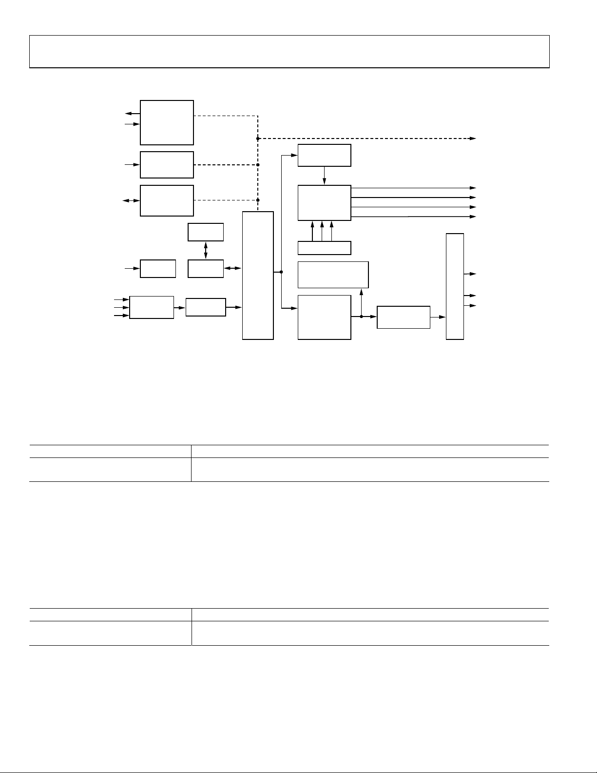
HDMI RECEIVER
HPA_A/INT2
RXA_5V
CEC
DDCA_SDA/DDCA_SC L
RXA_C±
RXA_0±
RXA_1±
RXA_2±
5V DETECT
AND HPA
CONTROLLER
CEC
CONTROLLER
EDID/
REPEATER
CONTROLLER
PLL
HDCP
EEPROM
HDCP
BLOCK
SAMPLEREQUALIZER
TO INTERRUPT
CONTROL LER
DEEP COLOR
CONVERSION
DATA
4:2:2 TO 4:4:4
CONVERSION
FILTER
PACKET/
INFOF RAME
MEMORY
PACKET
HDMI DECODE + PORT MEASUREMENT
PROCESSOR
HS
VS
DE
AUDIO
PROCESSOR
AUDIO OUT POUT FORMATTER
TO DPP
TO DPP
TO DPP
TO DPP
AP
SCLK/INT2
MCLK/INT2
09238-004
Figure 3. Functional Block Diagram of HDMI Core
+5 V CABLE DETECT
The HDMI receiver in the ADV7611 can monitor the level on the +5 V power signal pin of the HDMI port. The results of this detection
can be read back from the following I
CABLE_DET_A_RAW, IO, Address 0x6F[0] (Read Only)
Raw status of Port A +5 V cable detection signal.
Function
CABLE_DET_A_RAW Description
0 (default) No cable detected on Port A
1 Cable detected on Port A (high level on RXA_5V)
The ADV7611 provides a digital glitch filter on the +5 V power signals from the HDMI port. The output of this filter is used to reset the
HDMI block (refer to the HDMI Section Reset Strategy section).
The +5 V power signal must be constantly high for the duration of the timer (controlled by FILT_5V_DET_TIMER[6:0]), otherwise the
output of the filter is low. The output of the filter returns low as soon as any change in the +5 V power signal is detected.
FILT_5V_DET_DIS, Addr 68 (HDMI), Address 0x56[7]
This control is used to disable the digital glitch filter on the HDMI 5 V detect signals. The filtered signals are used as interrupt flags and
used to reset the HDMI section. The filter works from an internal ring oscillator clock and, therefore, is available in power-down mode.
The clock frequency of the ring oscillator is 42 MHz ± 10%.
Function
FILT_5V_DET_DIS Description
0 (default) Enabled
1 Disabled
Note: If the +5 V pins are not used and are left unconnected, the +5 V detect circuitry must be disconnected from the HDMI reset signal
by setting DIS_CABLE_DET_RST to 1. This avoids holding the HDMI section in reset.
2
C registers. These readbacks are valid even when the part is not configured for HDMI mode.
Rev. A | Page 28 of 184
Page 29

Hardware User Guide UG-180
FILT_5V_DET_TIMER[6:0], Addr 68 (HDMI), Address 0x56[6:0]
This control is used to set the timer for the digital glitch filter on the HDMI +5 V detect inputs. The unit of this parameter is two clock
cycles of the ring oscillator (~ 47 ns). The input must be constantly high for the duration of the timer; otherwise, the filter output remains
low. The output of the filter returns low as soon as any change in the +5 V power signal is detected.
Function
FILT_5V_DET_TIMER[6:0] Description
1011000 (default) Approximately 4.2 μs
xxxxxxx Time duration of +5 V deglitch filter. Unit of this parameter is 2 clock cycles of the ring oscillator (~47 ns).
DIS_CABLE_DET_RST, Addr 68 (HDMI), Address 0x48[6]
This control disables the reset effects of cable detection. DIS_CABLE_DET_RST must be set to 1 if the +5 V pins are unused and left
unconnected.
Function
DIS_CABLE_DET_RST Description
0 (default)
1 Does not use 5 V input pins as reset signal for HDMI section
HOT PLUG ASSERT
The ADV7611 features hot plug assert (HPA) control for its HDMI port. The purpose of the control and its corresponding output pin is
to communicate to an HDMI transmitter that it is possible to access the enhanced-extended display identification (E-EDID) connected to
the DDC bus.
HPA_MANUAL, Addr 68 (HDMI), Address 0x6C[0]
Manual control enable for the HPA output pins. Automatic control of these pins is disabled by setting this bit. Manual control is
determined by the HPA_MAN_VALUE_X (where X = A).
Function
HPA_MANUAL Description
0 (default) HPA takes its value based on HPA_AUTO_INT_EDID
1 HPA takes its value from HPA_MAN_VALUE_X
HPA_MAN_VALUE_A, IO, Address 0x20[7]
A manual control for the value of HPA on Port A. Valid only if HPA_MANUAL is set to 1.
Function
HPA_MAN_VALUE_A Description
0 0 V applied to HPA_A pin
1 (default) High level applied to HPA_A pin
Note: The HPA_A pin is open drain. An external pull-up resistor is required to pull it high.
Resets HDMI section if 5 V input pin corresponding to selected HDMI port (for example, RXA_5V for Port A)
is inactive
Rev. A | Page 29 of 184
Page 30

UG-180 Hardware User Guide
HPA_AUTO_INT_EDID[1:0], Addr 68 (HDMI), Address 0x6C[2:1]
This control selects the type of automatic control on the HPA output pins. This bit has no effect when HPA_MANUAL is set to 1.
Function
HPA_AUTO_INT_EDID[1:0] Description
00
01 (default)
10 HPA of an HDMI port asserted high after two conditions met.
11 HPA of an HDMI port is asserted high after three conditions met:
Note: The delay is programmable via HPA_DELAY_SEL[3:0]. Refer to EDID_ENABLE for details on enabling the internal E-EDID for an
HDMI port. In HPA_MAN_VALUE_X and CABLE_DET_X_RAW, X refers to A.
HPA_DELAY_SEL[3:0], Addr 68 (HDMI), Address 0x6C[7:4]
Sets a delay between +5 V detection and hot plug assertion on the HPA output pins, in increments of 100 ms per bit.
Function
HPA_DELAY_SEL[3:0] Description
0000 No delay
0001 100 ms delay
0010 200 ms delay
1010 (default) 1 sec delay
1111 1.5 sec delay
HPA_TRISTATE_A, IO, Address 0x20[3]
Tristates HPA output pin for Port A.
Function
HPA_TRISTATE_A Description
0 (default) HPA_A pin active
1 Tristates HPA_A pin
HPA_STATUS_PORT_A, IO, Address 0x21[3] (Read Only)
Readback of HPA status for Port A.
Function
HPA_STATUS_PORT_A Description
0 (default) +5 V not applied to HPA_A pin by chip
1 +5 V applied to HPA_A pin by chip
HPA of an HDMI port asserted high immediately after internal EDID activated for that port. HPA of a specific
HDMI port deasserted low immediately after internal E-EDID is de-activated for that port.
HPA of an HDMI port asserted high following a programmable delay after part detects an HDMI cable plug
on that port. HPA of an HDMI port immediately deasserted after part detects a cable disconnect on that
HDMI port.
1. Internal EDID is active for that port.
2. Delayed version of cable detect signal CABLE_DET_X_RAW for that port is high.
HPA of an HDMI port immediately deasserted after either of these two conditions are met:
1. Internal EDID is de-activated for that port.
2. Cable detect signal CABLE_DET_X_RAW for that port is low.
1. Internal EDID is active for that port.
2. Delayed version of cable detect signal CABLE_DET_X_RAW for that port is high.
3. User has set manual HPA control for that port to 1 via HPA_MAN_VALUE_X controls.
HPA of an HDMI port immediately deasserted after any of these three conditions met:
1. Internal EDID de-activated for that port.
2. Cable detect signal CABLE_DET_X_RAW for that port is low.
3. User sets the manual HPD control for that port to 0 via HPA_MAN_VALUE_X controls
Rev. A | Page 30 of 184
Page 31

Hardware User Guide UG-180
HPA_OVR_TERM, Addr 68 (HDMI), Address 0x6C[3]
A control to set the termination control to be overridden by the HPA setting. When this bit is set, termination on a specific port is set
according to the HPA status of that port.
Function
HPA_OVR_TERM Description
0 (default) Automatic or manual I2C control of port termination
1 Termination controls disabled and overridden by HPA controls
E-EDID/REPEATER CONTROLLER
The HDMI section incorporates an E-EDID/repeater controller, which performs the following tasks:
• Computes the E-EDID checksum
• Performs the repeater routines described in the Repeater Support section
The E-EDID/repeater controller is powered from the DVDD supply and clocked by an internal ring oscillator. The controller and the
internal DDC bus arbiter are kept active in power-down Mode 0 and power-down Mode 1. This allows the internal E-EDID to be
functional and accessible through the DDC port, even when the part is powered down (refer to the Power-Down Modes section).
These HDMI transmitters can then read the capabilities of the powered-down application integrating the ADV7611 by accessing its
internal E-EDID through the DDC ports.
The E-EDID/repeater controller is reset when the DVDD supplies go low or when HDCP_REPT_EDID_RESET is set high. When the
E-EDID/repeater controller reboots, it performs the following tasks:
• Clears the internal E-EDID and Key Selection Vector (KSV) RAM (refer to E-EDID Data Configuration section and the Internal
HDCP Key OTP ROM section )
• Computes a checksum for port
HDCP_REPT_EDID_RESET, Addr 68 (HDMI), Address 0x5A[3] (Self-Clearing)
A reset control for the E-EDID/repeater controller. When asserted, it resets the E-EDID/repeater controller.
Function
HDCP_REPT_EDID_RESET Description
0 (default) Normal operation
1 Resets the E-EDID/repeater controller
E-EDID DATA CONFIGURATION
The ADV7611 features a RAM that can store an E-EDID. This internal E-EDID feature can be used for the HDMI port. It is also possible
to use an external device storage for the E-EDID data.
The following controls are provided to enable the internal E-EDID for each of the four HDMI ports.
EDID_A_ENABLE, Addr 64 (Repeater), Address 0x74[0]
Enables I
Function
EDID_A_ENABLE Description
0 (default) Disables E-EDID for Port A
1 Enables E-EDID for Port A
When the internal E-EDID is enabled, the ADV7611 must first calculate the E-EDID checksums for that port before the E-EDID is
actually enabled.
The following read only flags can be utilized to determine if the E-EDID is actually enabled on the HDMI ports.
EDID_A_ENABLE_CPU, Addr 64 (Repeater), Address 0x76[0] (Read Only)
Flags internal EDID enabling on Port A.
Function
EDID_A_ENABLE_CPU Description
0 (default) Disabled
1 Enabled
2
C access to the internal EDID RAM from DDC Port A.
Rev. A | Page 31 of 184
Page 32

UG-180 Hardware User Guide
Notes
• If the internal E-EDID RAM is enabled, an external E-EDID storage device must not be connected on the DDC bus of that port.
• The internal E-EDID can be read by current address read sequences on the DDC port.
• The ADV7611 supports the segment pointer, which is set at Register Address 0x60 through the DDC bus, and used in combination
with the internal E-EDID address (0xA0) to access the internal E-EDID.
• The contents of the EDID RAM are not to be trusted after power-up or hardware reset. Usersshould write the proper contents to the
EDID RAM memory inside the ADV7611 via an external MCU.
E-EDID Support for Power-Down Modes
The ADV7611 supports E-EDID access in Power-Down Mode 0 and Power-Down Mode 1. Using this feature, an application that
integrates the ADV7611 in standby can make its E-EDID available to the HDMI transmitter. This allows support of CEC and provides
compatibility with HDMI transmitters that require the E-EDID to be available when the HDMI receiver is powered down.
In Power-Down Mode 0, the part operates in a very low power state with only the minimum of internal circuitry enabled for the
internal E-EDID.
For more details on E-EDID accessibility in power-down modes, refer to the Power-Down Modes section.
TRANSITIONING OF POWER MODES
If the part starts in Power-Down Mode 0 and then transitions into a different power mode (that is, Power-Down Mode 1 or normal
operation mode), the information in the internal E-EDID is not overwritten. The internal E-EDID remains active on the HDMI port for
which the E-EDID has been accessed. This prevents disturbing E-EDID read requests from HDMI sources connected to the ADV7611
while it is being powered on, or while the power mode is transitioning.
It is possible to disable the automatic enable of internal EDID on the HDMI port when the part comes out of power-down mode, by
setting the DISABLE_AUTO_EDID bit.
DISABLE_AUTO_EDID, Addr 64 (Repeater), Address 0x7A[1]
Disables all automatic enables for internal E-EDID.
Function
DISABLE_AUTO_EDID Description
0 (default) Automatic enable of internal E-EDID on HDMI port when the part comes out of Power-Down Mode 0
1 Disable automatic enable of internal E-EDID on HDMI port when the part comes out of Power-Down Mode 0
STRUCTURE OF INTERNAL E-EDID
This section describes the structure of the internal E-EDID accessible through the DDC bus. This section describes the structure
and configuration for of the internal E-EDID accessed through Port A. The internal E-EDID is enabled for Port A by setting the
EDID_A_ENABLE bit to 1.
The structure of the internal E-EDID image for Port A is shown in Figure 4.
Rev. A | Page 32 of 184
Page 33

Hardware User Guide UG-180
Figure 4. Port A E-EDID Structure and Mapping for SPA Located in EDID Block 1
PORTAE-EDID STRUCTURE
BLOCK 2 CHECKSUM0x1FF
BLOCK 3
0x180
0x17F
BLOCK 2 CHECKSUM
BLOCK 2
0x100
0xFF
BLOCK 1 CHECKSUM
BLOCK 1
0x80
0x7F
BLOCK 0 CHECKSUM
BLOCK 0
0x00
0x1FE
0x17E
0xFE
0x7E
09238-005
Notes
• After EDID_A_ENABLE is set to 1, the ADV7611 EDID/repeater controller computes the checksums and updates the internal RAM
address locations 0x7F, 0xFF, 0X17F, and 0x1FF in the internal EDID RAM with the computed checksums.
• After power up, the ADV7611 E-EDID controller sets all bytes in the internal EDID RAM to 0, this operation takes less than 1 ms. It
is recommended to wait for at least 1 ms before initializing the EDID map with E-EDID.
• When internal E-EDID is enabled on Port A, the hot plug should not be asserted until the EDID map has been completely initialized
with E-EDID.
• The internal E-EDID can be accessed in read-only mode through the DDC interface at the I
• The internal E-EDID can be accessed in read/write mode through the general I
2
C interface at the EDID map I2C address.
2
C address 0xA0.
TMDS EQUALIZATION
The ADV7611 incorporates active equalization of the HDMI data signals. This equalization compensates for the high frequency losses
inherent in HDMI and DVI cabling, especially at long lengths and higher frequencies. The ADV7611 is capable of equalizing for cable
lengths up to 30 meters and for pixel clock frequencies up to 225 MHz.
PORT SELECTION
HDMI_PORT_SELECT allows the selection of the active HDMI port. The only port on ADV7611 is Port A.
HDMI_PORT_SELECT[2:0], Addr 68 (HDMI), Address 0x00[2:0]
This two bit control is used for HDMI primary port selection.
Function
HDMI_PORT_SELECT[2:0] Description
000 (default) Port A
TMDS CLOCK ACTIVITY DETECTION
The ADV7611 provides circuitry to monitor TMDS clock activity on HDMI port. The firmware can poll the appropriate registers for
TMDS clock activity detection and configure the ADV7611 as desired. TMDS clock detection control is active as soon as the ADV7611
detects activity above 25 MHz on the TMDS clock input.
Rev. A | Page 33 of 184
Page 34

UG-180 Hardware User Guide
TMDS_CLK_A_RAW, IO, Address 0x6A[4] (Read Only)
Raw status of Port A TMDS clock detection signal.
Function
TMDS_CLK_A_RAW Description
0 (default) No TMDS clock detected on Port A
1 TMDS clock detected on Port A
Important
• The clock detection flag is valid if the part is powered up or in Power Down Mode 1. Refer to the Power-Down Mode 1 section.
• The clock detection flags is valid, irrespective of the mode the part is set into via the PRIM_MODE[3:0] register.
Clock and Data Termination Control
The ADV7611 provides controls for the TMDS clock and data termination on the HDMI port.
Note: The clock termination of the port by HDMI_PORT_SELECT[2:0] must always be enabled.
This part does not support HDMI streams with a clock lower than 25 MHz.
TERM_AUTO, Addr 68 (HDMI), Address 0x01[0]
This bit allows the user to select automatic or manual control of clock termination. If automatic mode termination is enabled, then the
termination on the port selected via HDMI_PORT_SELECT[1:0] is enabled.
Function
TERM_AUTO Description
0 (default) Disable termination automatic control
1 Enable termination automatic control
Note: When manual mode is enabled, the termination for each port is set individually by the CLOCK_TERMA_DISABLE control bits
CLOCK_TERMA_DISABLE, Addr 68 (HDMI), Address 0x83[0]
Disable clock termination on Port A. Can be used when TERM_AUTO set to 0
Function
CLOCK_TERMA_DISABLE Description
0 Enable Termination Port A
1 (default) Disable Termination Port A
HDMI/DVI STATUS BITS
HDMI/DVI status mode is available through HDMI_MODE.
HDMI_MODE_RAW, Addr 68 (HDMI), Address 0x65[3] (Read Only)
Raw status signal of HDMI mode signal.
Function
HDMI_MODE_RAW Description
0 (default) DVI mode detected
1 HDMI mode detected
HDMI_MODE, Addr 68 (HDMI), Address 0x05[7] (Read Only)
A readback to indicate whether the stream processed by the HDMI core is a DVI or an HDMI stream.
Function
HDMI_MODE Description
0 (default) DVI mode detected
1 HDMI mode detected
VIDEO 3D DETECTION
Status of 3D video is available through the VIDEO_3D_RAW bit.
VIDEO_3D_RAW, Addr 68 (HDMI), Address 0x6A[2] (Read Only)
Raw status of the video 3D signal.
Rev. A | Page 34 of 184
Page 35

Hardware User Guide UG-180
Function
VIDEO_3D_RAW Description
0 Video 3D not detected (read only)
1 Video 3D detected
TMDS MEASUREMENT
The ADV7611 contains logic that measures the frequency of the TMDS clock transmitted. The TMDS frequency can be read back via the
TMDSFREQ[8:0] and TMDSFREQ_FRAC[6:0] registers.
TMDS Measurement after TMDS PLL
The TMDSFREQ measurement is provided by a clock measurement circuit located after the TMDS PLL. The TMDS PLL must, therefore,
be locked to the incoming TMDS clock in order for the TMDSFREQ and TMDSFREQ_FRAC registers to return a valid measurement.
The TMDS frequency can be obtained using Equation 1, TMDS Frequency in MHz (Measured after TMDS PLL).
TMDS
TMDSFREQF
_ FRACTMDSFREQ
128
Notes
The TMDS PLL lock status can be monitored via TMDS_PLL_LOCKED.
The TMDS_PLL_LOCKED flag should be considered valid if a TMDS clock is input on the HDMI port selected via
HDMI_PORT_SELECT[2:0].
The NEW_TMDS_FRQ_RAW flag can be used to monitor if the TMDS frequency on the selected HDMI port changes by a
programmable threshold.
(1)
The ADV7611 can be configured to trigger an interrupt when the bit NEW_TMDS_FRQ_RAW changes from 0 to 1. In that
configuration, the interrupt status NEW_TMDS_FRQ_ST indicates that NEW_TMDS_FRQ_RAW has changed from 0 to 1. Refer to the
Interrupts section for additional information on the configuration of interrupts.
TMDSFREQ[8:0], Addr 68 (HDMI), Address 0x51[7:0]; Address 0x52[7] (Read Only)
This register provides a full precision integer TMDS frequency measurement.
Function
TMDSFREQ[8:0] Description
000000000 (default) Outputs 9-bit TMDS frequency measurement in MHz
xxxxxxxxx Outputs 9-bit TMDS frequency measurement in MHz
TMDSFREQ_FRAC[6:0], Addr 68 (HDMI), Address 0x52[6:0] (Read Only)
A readback to indicate the fractional bits of measured frequency of PLL recovered TMDS clock. The unit is 1/128 MHz.
Function
TMDSFREQ_FRAC[6:0] Description
0000000 (default) Outputs 7-bit TMDS fractional frequency measurement in 1/128 MHz
xxxxxxx Outputs 7-bit TMDS fractional frequency measurement in 1/128 MHz
TMDS_PLL_LOCKED, Addr 68 (HDMI), Address 0x04[1] (Read Only)
A readback to indicate if the TMDS PLL is locked to the TMDS clock input to the selected HDMI port.
Function
TMDS_PLL_LOCKED Description
0 (default) The TMDS PLL is not locked.
1 The TMDS PLL is locked to the TMDS clock input to the selected HDMI port.
TMDSPLL_LCK_A_RAW, IO, Address 0x6A[6] (Read Only)
A readback to indicate the raw status of the Port A TMDS PLL lock signal.
Function
TMDSPLL_LCK_A_RAW Description
0 (default) TMDS PLL on Port A is not locked.
1 TMDS PLL on Port A is locked to the incoming clock.
Rev. A | Page 35 of 184
Page 36

UG-180 Hardware User Guide
NEW_TMDS_FRQ_RAW, IO, Address 0x83[1] (Read Only)
Status of new TMDS frequency interrupt signal. When set to 1, it indicates the TMDS Frequency has changed by more than the tolerance
set in FREQTOLERANCE[3:0]. Once set, this bit will remain high until it is cleared via NEW_TMDS_FREQ_CLR.
Function
NEW_TMDS_FRQ_RAW Description
0 (default) TMDS frequency has not changed by more than tolerance set in FREQTOLERANCE[3:0] in the HDMI map.
1 TMDS frequency has changed by more than tolerance set in FREQTOLERANCE[3:0] in the HDMI map.
FREQTOLERANCE[3:0], Addr 68 (HDMI), Address 0x0D[3:0]
Sets the tolerance in MHz for new TMDS frequency detection. This tolerance is used for the audio mute mask MT_MSK_VCLK_CHNG
and the HDMI status bit NEW_TMDS_FRQ_RAW.
Function
FREQTOLERANCE[3:0] Description
0100 (default) Default tolerance in MHz for new TMDS frequency detection
xxxx Tolerance in MHz for new TMDS frequency detection
DEEP COLOR MODE SUPPORT
The Deep Color mode information that the ADV7611 extracts from the general control packet can be read back from
DEEP_COLOR_MODE[1:0].
DEEP_COLOR_MODE[1:0], Addr 68 (HDMI), Address 0x0B[7:6] (Read Only)
A readback of the Deep Color mode information extracted from the general control packet
Function
DEEP_COLOR_MODE[1:0] Description
00 (default) 8-bits per channel
01 10-bits per channel
10 12-bits per channel
Notes
• Deep Color mode can be monitored via DEEP_COLOR_CHNG_RAW, which indicates if the color depth of the processed HDMI
stream has changed.
•
The ADV7611 can be configured to trigger an interrupt when the DEEP_COLOR_CHNG_RAW bit changes from 0 to 1. In that
configuration, the interrupt status DEEP_COLOR_CHNG_ST indicates that DEEP_COLOR_CHNG_RAW has changed from 0 to 1.
Refer to the Interrupts section for additional information on the configuration of interrupts.
DEEP_COLOR_CHNG_RAW, IO, Address 0x83[7] (Read Only)
Status of Deep Color mode changed interrupt signal. When set to 1 it indicates a change in the deep color mode has been detected. Once
set, this bit will remain high until it is cleared via DEEP_COLOR_CHNG_CLR.
Function
DEEP_COLOR_CHNG_RAW Description
0 (default) Deep color mode has not changed
1 Change in deep color triggered this interrupt
VIDEO FIFO
The ADV7611 contains a FIFO located between the incoming TMDS data and the CP core (refer to Figure 5). Data arriving over the
HDMI link will be at 1X for non-Deep Color mode (8 bits per channel), and 1.25X, 1.5X, or 2X for deep color modes (30, 36, and 48 bits,
respectively). Data unpacking and data rate reduction must be performed on the incoming HDMI data to provide the CP core with the
correct data rate and data bit width. The video FIFO is used to pass data safely across the clock domains.
The video FIFO also provides extreme robustness to jitter on the TMDS clock. The CP clock is generated by a DPLL running on the
incoming TMDS clock, and the CP clock may contain less jitter than the incoming TMDS clock. The video FIFO provides immunity to
the incoming jitter and the resultant clock phase mismatch between the CP clock and the TMDS clock.
Rev. A | Page 36 of 184
Page 37

Hardware User Guide UG-180
TMDS
CLOCK
TMDS
CHANNEL 0
TMDS
CHANNEL 1
TMDS
CHANNEL 2
TMDS
PLL
TMDS
SAMPLING
AND
DATA
RECOVERY
TMDS CH0
10
TMDS CH1
10
TMDS CH2
10
TMDS
DECODING
DIVIDE R
R
G
B
HS
VS
DE
DPLL
12
12
12
FIFO
R
G
B
HS
VS
DE
12
12
12
09238-009
Figure 5. HDMI Video FIFO
The video FIFO is designed to operate completely autonomously. It automatically resynchronizes the read and write pointers if they are
about to point to the same location. However, it is also possible for the user to observe and control the FIFO operation with a number of
FIFO status and control registers.
DCFIFO_LEVEL[2:0], Addr 68 (HDMI), Address 0x1C[2:0] (Read Only)
A readback that indicates the distance between the read and write pointers. Overflow/underflow would read as Level 0. Ideal centered
functionality would read as 0b100.
Function
DCFIFO_LEVEL[2:0] Description
000 (default) FIFO has underflowed or overflowed.
001 FIFO is about to overflow.
010 FIFO has some margin.
011 FIFO has some margin.
100 FIFO perfectly balanced
101 FIFO has some margin.
110 FIFO has some margin.
111 FIFO is about to underflow.
DCFIFO_LOCKED, Addr 68 (HDMI), Address 0x1C[3] (Read Only)
A readback to indicate if video FIFO is locked.
Function
DCFIFO_LOCKED Description
0 (default) Video FIFO is not locked. Video FIFO had to resynchronize between previous two Vsyncs.
1 Video FIFO is locked. Video FIFO did not have to resynchronize between previous two Vsyncs.
DCFIFO_RECENTER, Addr 68 (HDMI), Address 0x5A[2] (Self-Clearing)
A reset to recenter the video FIFO. This is a self-clearing bit.
Function
DCFIFO_RECENTER Description
0 (default) Video FIFO normal operation
1 Video FIFO to recenter
Rev. A | Page 37 of 184
Page 38

UG-180 Hardware User Guide
DCFIFO_KILL_DIS, Addr 68 (HDMI), Address 0x1B[2]
The video FIFO output is zeroed if there is more than one resynchronization of the pointers within two FIFO cycles. This behavior can be
disabled with this bit.
Function
DCFIFO_KILL_DIS Description
0 (default) FIFO output set to zero if more than one resynchronization is necessary during two FIFO cycles
1 FIFO output never set to zero regardless of how many resynchronizations occur
DCFIFO_KILL_NOT_LOCKED, Addr 68 (HDMI), Address 0x1B[3]
DCFIFO_KILL_NOT_LOCKED controls whether or not the output of the Video FIFO is set to zero when the video PLL is unlocked.
Function
DCFIFO_KILL_NOT_LOCKED Description
0 FIFO data is output regardless of video PLL lock status.
1 (default) FIFO output is zeroed if video PLL is unlocked.
The DCFIFO is programmed to reset itself automatically when the video PLL transitions from unlocked to locked. Note that the video
PLL transition does not necessarily indicate that the overall system is stable.
DCFIFO_RESET_ON_LOCK, Addr 68 (HDMI), Address 0x1B[4]
Enables the reset/recentering of video FIFO on video PLL unlock
Function
DCFIFO_RESET_ON_LOCK Description
0 Do not reset on video PLL lock
1 (default) Reset FIFO on video PLL lock
PIXEL REPETITION
In HDMI mode, video formats with TMDS rates below 25 M pixels/sec require pixel repetition in order to be transmitted over the TMDS
link. When the ADV7611 receives this type of video format, it discards repeated pixel data automatically, based on the pixel repetition
field available in the AVI InfoFrame.
When HDMI_PIXEL_REPETITION is nonzero, video pixel data is discarded and the pixel clock frequency is divided by
(HDMI_PIXEL_REPETITION) + 1.
HDMI_PIXEL_REPETITION[3:0], Addr 68 (HDMI), Address 0x05[3:0] (Read Only)
A readback to provide the current HDMI pixel repetition value decoded from the AVI InfoFrame received. The HDMI receiver
automatically discards repeated pixel data and divides the pixel clock frequency appropriately as per the pixel repetition value.
Function
HDMI_PIXEL_REPETITION[3:0] Description
0000 (default) 1×
0001 2×
0010 3×
0011 4×
0100 5×
0101 6×
0110 7×
0111 8×
1000 9×
1001 10×
1010 to 1111 Reserved
Rev. A | Page 38 of 184
Page 39

Hardware User Guide UG-180
DEREP_N_OVERRIDE, Addr 68 (HDMI), Address 0x41[4]
This control allows the user to override the pixel repetition factor. The ADV7611 then uses DEREP_N instead of
HDMI_PIXEL_REPETITION[3:0] to discard video pixel data from the incoming HDMI stream.
Function
DEREP_N_OVERRIDE Description
0 (default)
1 Enables manual setting of the pixel repetition factor as per DEREP_N[3:0].
DEREP_N[3:0], Addr 68 (HDMI), Address 0x41[3:0]
Sets the derepetition value if derepetition is overridden by setting DEREP_N_OVERRIDE.
Function
DEREP_N[3:0] Description
0000 (default) DEREP_N+1 indicates the pixel and clock discard factor
xxxx DEREP_N+1 indicates the pixel and clock discard factor
The following registers allow forcing YCrCb 444 and YCrCb 422 regardless of the AVI Infoframe. This feature is useful when the source
switches between YCrCb 444 and YCrCb 422 modes without sending appropriate update in AVI Infoframe.
FORCE_YCRCB_444, Addr 68 (HDMI), Address 0x46[4]
Forces a 4:4:4 interpretation of the video contents, regardless of the description in the AVI infoframe. This bit carries higher priority than
FORCE_YCRCB_422.
Function
FORCE_YCRCB_444 Description
0 (default) Not forced
1 Forced
FORCE_YCRCB_422, Addr 68 (HDMI), Address 0x47[4]
Forces a 4:2:2 interpretation of the video contents, regardless of the description in the AVI infoframe. This bit is only valid if
FORCE_YCRCB_444 is zero.
Function
FORCE_YCRCB_422 Description
0 (default) Not forced
1 Forced
HDCP SUPPORT
HDCP Decryption Engine
The HDCP decryption engine allows for the reception and decryption of HDCP content-protected video and audio data. In the HDCP
authentication protocol, the transmitter authenticates the receiver by accessing the HDCP registers of the ADV7611 over the DDC bus.
Once the authentication is initiated, the HDCP decryption integrated in the ADV7611 computes and updates a decryption mask for every
video frame. This mask is applied to the incoming data at every clock cycle to yield decrypted video and audio data.
HDCP_A0, Addr 68 (HDMI), Address 0x00[7]
A control to set the second LSB of the HDCP port I
Function
HDCP_A0 Description
0 (default) I2C address for HDCP port is 0x74. Used for single-link mode or 1st Receiver in dual-link mode.
1 I2C address for HDCP port is 0x76. Used only for a second receiver dual-link mode.
Automatic detection and processing of procession of pixel repeated modes using the AVI InfoFrame
information.
2
C address.
Rev. A | Page 39 of 184
Page 40

UG-180 Hardware User Guide
HDMI_CONTENT_ENCRYPTED, Addr 68 (HDMI), Address 0x05[6] (Read Only)
A readback to indicate the use of HDCP encryption.
Function
HDMI_CONTENT_ENCRYPTED Description
0 (default) The input stream processed by the HDMI core is not HDCP encrypted.
1 The input stream processed by the HDMI core is HDCP encrypted.
HDMI_ENCRPT_X_RAW reports the encryption status of the data present on each individual HDMI port (where X = A).
Note: These bits are reset to 0 if an HDMI packet detection reset occurs. (Refer to the HDMI Packet Detection Flag Reset section.)
HDMI_ENCRPT_A_RAW, IO, Address 0x6F[2] (Read Only)
Raw status of Port A encryption detection signal.
Function
HDMI_ENCRPT_A_RAW Description
0 (default) Current frame in Port A is not encrypted.
1 Current frame in Port A is encrypted.
Notes
• The ADV7611 supports the 1.1_FEATURES, FAST_REAUTHENTICATION, and FAST_I2C speed HDCP features. The BCAPS
register must be initialized appropriately if these features are to be supported by the application integrating the ADV7611, for
example, set BCAPS[0] to 1 to support FAST_REAUTHENTICATION.
•
It is recommended to set BCAPS[7:0] Bit [7] to 1 if the ADV7611 is used as the front end of an HDMI receiver. This bit should be set
to 0 for DVI applications.
Internal HDCP Key OTP ROM
The ADV7611 features an on-chip nonvolatile memory that is preprogrammed with a set of HDCP keys.
HDCP Keys Access Flags
The ADV7611 accesses the internal HDCP key OTP ROM (also referred to as HDCP ROM) on two different occasions:
•
After a power up, the ADV7611 reads the KSV from the internal HDCP ROM (refer to Figure 6).
•
After a KSV update from an HDCP transmitter, the ADV7611 reads the KSV and all keys in order to carry out the link verification
response (refer to Figure 7).
The host processor can read the HDCP_KEYS_READ and HDCP_KEY_ERROR flags to check that the ADV7611 successfully accessed
the HDCP ROM.
HDCP_KEYS_READ, Addr 68 (HDMI), Address 0x04[5] (Read Only)
A readback to indicate a successful read of the HDCP keys and/or KSV from the internal HDCP Key OTP ROM. A logic high is returned
when the read is successful.
Function
HDCP_KEYS_READ Description
0 (default) HDCP keys and/or KSV not yet read
1 HDCP keys and/or KSV HDCP keys read
HDCP_KEY_ERROR, Addr 68 (HDMI), Address 0x04[4] (Read Only)
A readback to indicate if a checksum error occurred while reading the HDCP and/or KSV from the HDCP Key ROM Returns 1 when
HDCP Key master encounters an error while reading the HDCP Key OTP ROM
Function
HDCP_KEY_ERROR Description
0 (default) No error occurred while reading HDCP keys
1 HDCP keys read error
Rev. A | Page 40 of 184
Page 41

Hardware User Guide UG-180
START
(AFTER POWER-UP)
HDCP_KEY_READ = 0
HDCP_KEY_ERROR = 0
READ KSV AND CHECKSUM
CS1 FROM HDC P OTP ROM
DERIVE CHECKSUM CS1'
FROM KSV
CS1 = CS1'
YES
SET BKSV (HDC P REGISTER
ADDRESS 0x00
BKSV = KSV
HDCP_KEY_READ = 1
HDCP_KEY_ERROR = 0
END
NO
HDCP_KEY_ERROR = 1
09238-010
Figure 6. HDCP ROM Access After Power-Up
Rev. A | Page 41 of 184
Page 42

UG-180 Hardware User Guide
START
(AKSV UPDATE
FROM TRANSMITTER)
HDCP_KEY_READ = 0
HDCP_KEY_ERROR = 0
READ KSV, HDCP KEYS AND
CHECKSUM CS2 FRO M HDCP PROM
DERIVE CHECKSUM CS2'
FROM KSV AND HDC P KEYS
CS1 = CS1'
YES
DERIVE LI NK VERIFICATION Ri'
UPDATE BKSV AND Ri' IN
HDCP RESGI STERS
HDCP_KEY_READ = 1
END
HDCP_KEY_ERROR = 0
END
Figure 7. HDCP ROM Access After KSV Update from the Transmitter
NO
HDCP_KEY_ERROR = 1
09238-011
Notes
• After the part has powered up, it is recommended to wait for 1 ms before checking the HDCP_KEYS_READ and
HDCP_KEY_ERROR flag bits. This ensures that the ADV7611 had sufficient time to access the internal HDCP ROM and set the
HDCP_KEYS_READ and HDCP_KEY_ERROR flag bits.
•
After an AKSV update from the transmitter, it is recommended to wait for 2 ms before checking the HDCP_KEYS_READ and
HDCP_KEY_ERROR flag bits. This ensures that the ADV7611 had sufficient time to access the internal HDCP ROM, and set the
HDCP_KEYS_READ and HDCP_KEY_ERROR flag bits.
•
When the ADV7611 successfully retrieves the HDCP keys and/or KSV from the internal HDCP ROM, the HDCP_KEYS_READ flag
bit is set to 1 and the HDCP_KEY_ERROR flag bit is set to 0.
•
The I
2
C controllers for the main I2C lines and the HDCP lines are independent of each other. It is, therefore, possible to access the
internal registers of the ADV7611 while it reads the HDCP keys and/or the KSV from the internal HDCP ROM.
•
A hardware reset (that is, reset via the reset pin) does not lead the ADV7611 to read the KSV or the keys from the HDCP ROM.
•
The ADV7611 takes 1.8 ms to read the keys from the HDCP ROM
HDCP Ri Expired
Following register allows early detection of HDMI TX failure. Also refer to interrupt status controls RI_EXPIRED_A_ST.
HDCP_RI_EXPIRED, Addr 68 (HDMI), Address 0x04[3] (Read Only)
Readback high when a calculated Ri has not been read by the source TX, on the active port. It remains high until next Aksv update.
Function
HDCP_RI_EXPIRED Description
0 (default) Calculated Ri has been read by the source TX
1 Calculated Ri has not been read by the source TX
Rev. A | Page 42 of 184
Page 43

Hardware User Guide UG-180
HDMI SYNCHRONIZATION PARAMETERS
The ADV7611 contains the logic required to measure the details of the incoming video resolution. The HDMI synchronization
parameters readback registers from the HDMI Map can be used, in addition to the STDI registers from the CP (refer to the Standard
Detection and Identification section), to estimate the video resolution of the incoming HDMI stream.
Notes
• The synchronization parameters are valid if the part is configured in HDMI mode via PRIM_MODE[3:0].
The HDMI synchronization filter readback parameters are valid even while the part free runs (refer to the Free Run Mode section)
•
on the condition that the measurement filters have locked.
Horizontal Filter and Measurements
The HDMI horizontal filter performs measurements on the DE and HSync of the HDMI stream on the selected port. These
measurements are available in the HDMI Map and can be used to determine the resolution of the incoming video data stream.
Primary Port Horizontal Filter Measurements
The HDMI horizontal filter performs the measurements described in this section on the HDMI port selected by
HDMI_PORT_SELECT[2:0].
Notes
• The horizontal measurements are valid only if DE_REGEN_LCK_RAW is set to 1.
The HDMI horizontal filter is used solely to measure the horizontal synchronization signals decoded from the HDMI stream. The
•
HDMI horizontal filter is not in the main path of the synchronization processed by the part and does not delay the overall HDMI
data into video data out latency.
•
The unit for horizontal filter measurement is a pixel, that is, the actual element of the picture content encapsulated in the HDMI/DVI
stream which the ADV7611 processes. A pixel has a duration T
measurements.
= T
T
Pixel
× DEEP_COLOR_RATIO × (PIXEL_REPETITION + 1) (2)
FTMDS
where:
T
is the TMDS frequency.
FTMDS
DEEP_COLOR_RATIO = 1 for 24-bit deep color.
DEEP_COLOR_RATIO = 5/4 for 30-bit deep color.
DEEP_COLOR_RATIO = 3/2 for 36-bit deep color.
DEEP_COLOR_RATIO = 2 for 48-bit deep color.
PIXEL_REPETITION is the number of repeated pixels in the input HDMI stream.
, which is provided in Equation 2, unit time of horizontal filter
PIXEL
DE_REGEN_FILTER_LOCKED, Addr 68 (HDMI), Address 0x07[5] (Read Only)
DE regeneration filter lock status. Indicates that the DE regeneration section has locked to the received DE and horizontal
synchronization parameter measurements are valid for readback.
Function
DE_REGEN_FILTER_LOCKED Description
0 (default) DE regeneration not locked
1 DE regeneration locked to incoming DE
DE_REGEN_LCK_RAW, IO, Address 0x6A[0] (Read Only)
Raw status of the DE regeneration lock signal.
Function
DE_REGEN_LCK_RAW Description
0 (default) DE regeneration block has not been locked.
1 DE regeneration block has been locked to the incoming DE signal.
Rev. A | Page 43 of 184
Page 44

UG-180 Hardware User Guide
TOTAL_LINE_WIDTH[13:0], Addr 68 (HDMI), Address 0x1E[5:0]; Address 0x1F[7:0] (Read Only)
Total line width is a horizontal synchronization measurement. This gives the total number of pixels per line. This measurement is valid
only when the DE regeneration filter has locked.
Function
TOTAL_LINE_WIDTH[13:0] Description
xxxxxxxxxxxxx Total number of pixels per line
LINE_WIDTH[12:0], Addr 68 (HDMI), Address 0x07[4:0]; Address 0x08[7:0] (Read Only)
Line width is a horizontal synchronization measurement, which gives the number of active pixels in a line. This measurement is only valid
when the DE regeneration filter is locked.
Function
LINE_WIDTH[12:0] Description
00000000000 (default) Total number of active pixels per line
xxxxxxxxxxx Total number of active pixels per line
HSYNC_FRONT_PORCH[12:0], Addr 68 (HDMI), Address 0x20[4:0]; Address 0x21[7:0] (Read Only)
HSync front porch width is a horizontal synchronization measurement. The unit of this measurement is unique pixels. This measurement
is valid only when the DE regeneration filter has locked.
Function
HSYNC_FRONT_PORCH[12:0] Description
xxxxxxxxxxx Total number of pixels in the front porch
HSYNC_PULSE_WIDTH[12:0], Addr 68 (HDMI), Address 0x22[4:0]; Address 0x23[7:0] (Read Only)
HSync pulse width is a horizontal synchronization measurement. The unit of this measurement is unique pixels. This measurement is
valid only when the DE regeneration filter has locked.
Function
HSYNC_PULSE_WIDTH[12:0] Description
xxxxxxxxxxx Total number of pixels in the hsync pulse
HSYNC_BACK_PORCH[12:0], Addr 68 (HDMI), Address 0x24[4:0]; Address 0x25[7:0] (Read Only)
HSync back porch width is a horizontal synchronization measurement. The unit of this measurement is unique pixels. This measurement
is valid only when the DE regeneration filter has locked.
Function
HSYNC_BACK_PORCH[12:0] Description
xxxxxxxxxxx Total number of pixels in the back porch
DVI_HSYNC_POLARITY, Addr 68 (HDMI), Address 0x05[5] (Read Only)
A readback to indicate the polarity of the HSync encoded in the input stream
Function
DVI_HSYNC_POLARITY Description
0 (default) The HSync is active low.
1 The HSync is active high.
Rev. A | Page 44 of 184
Page 45

Hardware User Guide UG-180
DATA
ENABLE
D
C
HSYNC
NOTE:
A TOTAL NUMBER OF PIXELS PER LINE
B ACTIVE NUMBER OF PIXELS PER LINE
C HSYNC FRONT PO RCH WIDTH IN PIXEL UNIT
D HSYNC WIDTH IN PIXEL UNIT
E HSYNC BACK PORCH W IDTH IN PIXEL UNIT
Figure 8. Horizontal Timing Parameters
A
B
E
Horizontal Filter Locking Mechanism
The locking/unlocking mechanism of the HDMI horizontal filter is as follows:
The HDMI horizontal filter locks if the following two conditions are met:
•
•
The DE transitions occur at the exact same pixel count for eight consecutive video lines
•
The HSync transitions occur at the exact same pixel count for eight consecutive video lines
•
The HDMI horizontal filter unlocks if either of the two following conditions are met:
•
The DE transitions occur on different pixels count for 15 consecutive video lines
The HSync transitions occur on different pixels count for 15 consecutive video lines
•
09238-012
Vertical Filters and Measurements
The ADV7611 integrates a HDMI vertical filter, which performs measurements on the VSync of the HDMI stream on the selected port.
These measurements are available in the HDMI map and can be used to determine the resolution of the incoming video data stream.
Primary Port Vertical Filter Measurements
The HDMI vertical filter performs the measurements on the HDMI port selected by HDMI_PORT_SELECT[2:0].
The Field 0 measurements are adequate to determine the standard of incoming progressive modes. A combination of Field 0 and field 1
measurements should be used to determine the standard of interlaced modes.
Notes
• The vertical measurements are valid only if V_LOCKED_RAW is set to 1.
•
The HDMI vertical filter is used solely to measure the vertical synchronization signals decoded from the HDMI stream. This filter is
not in the main path of the synchronization processed by the part and does not delay the overall HDMI data into video data out
latency.
VERT_FILTER_LOCKED, Addr 68 (HDMI), Address 0x07[7] (Read Only)
Vertical filter lock status. Indicates whether the vertical filter is locked and vertical synchronization parameter measurements are valid for
readback.
Function
VERT_FILTER_LOCKED Description
0 Vertical filter has not locked.
1 Vertical filter has locked.
V_LOCKED_RAW, IO, Address 0x6A[1] (Read Only)
Raw status of the vertical sync filter locked signal.
Function
V_LOCKED_RAW Description
0 Vertical sync filter has not locked and vertical sync parameters are not valid
1 Vertical sync filter has locked and vertical sync parameters are valid
Note: Field 0 measurements are used to determine the video modes that are progressive.
Rev. A | Page 45 of 184
Page 46

UG-180 Hardware User Guide
FIELD0_TOTAL_HEIGHT[13:0], Addr 68 (HDMI), Address 0x26[5:0]; Address 0x27[7:0] (Read Only)
Field 0 total height is a vertical synchronization measurement. This readback gives the total number of half lines in Field 0. This
measurement is valid only when the vertical filter has locked.
Function
FIELD0_TOTAL_HEIGHT[13:0] Description
xxxxxxxxxxxxxx The total number of half lines in Field 0 (divide readback by 2 to get number of lines)
FIELD0_HEIGHT[12:0], Addr 68 (HDMI), Address 0x09[4:0]; Address 0x0A[7:0] (Read Only)
Field 0 height is a vertical filter measurement. This readback gives the number of active lines in Field 0. This measurement is valid only
when the vertical filter has locked.
Function
FIELD0_HEIGHT[12:0] Description
xxxxxxxxxxxxx The number of active lines in Field 0
FIELD0_VS_FRONT_PORCH[13:0], Addr 68 (HDMI), Address 0x2A[5:0]; Address 0x2B[7:0] (Read Only)
Field 0 VSync front porch width is a vertical synchronization measurement. The unit of this measurement is half lines. This measurement
is valid only when the vertical filter has locked.
Function
FIELD0_VS_FRONT_PORCH[13:0] Description
xxxxxxxxxxxxxx
FIELD0_VS_PULSE_WIDTH[13:0], Addr 68 (HDMI), Address 0x2E[5:0]; Address 0x2F[7:0] (Read Only)
Field 0 VSync width is a vertical synchronization measurement. The unit for this measurement is half lines. This measurement is valid
only when the vertical filter has locked.
Function
FIELD0_VS_PULSE_WIDTH[13:0] Description
xxxxxxxxxxxxxx
FIELD0_VS_BACK_PORCH[13:0], Addr 68 (HDMI), Address 0x32[5:0]; Address 0x33[7:0] (Read Only)
Field 0 VSync back porch width is a vertical synchronization measurement. The unit for this measurement is half lines.
Function
FIELD0_VS_BACK_PORCH[13:0] Description
xxxxxxxxxxxxxx
DVI_VSYNC_POLARITY, Addr 68 (HDMI), Address 0x05[4] (Read Only)
A readback to indicate the polarity of the VSync encoded in the input stream
Function
DVI_VSYNC_POLARITY Description
0 The Vsync is active low.
1 The VSync is active high.
The total number of half lines in the VSync front porch of Field 0 (divide readback by 2 to get
number of lines)
The total number of half lines in the VSync pulse of Field 0 (divide readback by 2 to get number of
lines)
The total number of half lines in the VSync Back Porch of Field 0 (divide readback by 2 to get number
of lines)
Rev. A | Page 46 of 184
Page 47

Hardware User Guide UG-180
A
B
DATA
ENABLE
HSYNC
C
VSYNC
NOTE:
A TOTAL NUMBER OF LINES IN FIELD 0. UNIT IS IN HALF LINES.
B ACTIVES NUMBER O F LINES IN FIELD 0. UNIT IS IN HALF LINES.
C VSYNC FRONT PORCH WIDTH IN FI ELD 0. UNIT IS IN HALF LINES.
D VSYNC PULSE W IDTH IN FIELD 0. UNIT IS IN HAL F LINES.
E VSYNC BACK PO RCH WIDTH IN FIELD 0. UNIT IS I N HALF LINES.
Figure 9. Vertical Parameters for FIELD 0
Note: Field 1 measurements should not be used for progressive video modes.
FIELD1_TOTAL_HEIGHT[13:0], Addr 68 (HDMI), Address 0x28[5:0]; Address 0x29[7:0] (Read Only)
Field 1 total height is a vertical synchronization measurement. This readback gives the total number of half lines in Field 1.
This measurement is valid only when the vertical filter has locked. Field 1 measurements are valid when HDMI_INTERLACED
is set to 1.
Function
FIELD1_TOTAL_HEIGHT[13:0] Description
xxxxxxxxxxxxxx The total number of half lines in Field 1 (divide readback by 2 to get number of lines)
FIELD1_HEIGHT[12:0], Addr 68 (HDMI), Address 0x0B[4:0]; Address 0x0C[7:0] (Read Only)
Field 1 height is a vertical filter measurement. This readback gives the number of active lines in field. This measurement is valid only
when the vertical filter has locked. Field 1 measurements are only valid when HDMI_INTERLACED is set to 1.
Function
FIELD1_HEIGHT[12:0] Description
xxxxxxxxxxxxx The number of active lines in Field 1
FIELD1_VS_FRONT_PORCH[13:0], Addr 68 (HDMI), Address 0x2C[5:0]; Address 0x2D[7:0] (Read Only)
Field 1 VSync front porch width is a vertical synchronization measurement. The unit of this measurement is half lines. This measurement is
valid only when the vertical filter has locked. Field 1 measurements are valid when HDMI_INTERLACED is set to 1.
Function
FIELD1_VS_FRONT_PORCH[13:0] Description
xxxxxxxxxxxxxx
The total number of half lines in the VSync front porch of Field 1 (divide readback by 2 to get
number of lines)
FIELD1_VS_PULSE_WIDTH[13:0], Addr 68 (HDMI), Address 0x30[5:0]; Address 0x31[7:0] (Read Only)
Field 1 VSync width is a vertical synchronization measurement. The unit for this measurement is half lines. This measurement is valid
only when the vertical filter has locked. Field 1 measurements are valid when HDMI_INTERLACED is set to 1.
Function
FIELD1_VS_PULSE_WIDTH[13:0] Description
xxxxxxxxxxxxxx
The total number of half lines in the VSync pulse of Field 1 (divide readback by 2 to get number
of lines)
FIELD1_VS_BACK_PORCH[13:0], Addr 68 (HDMI), Address 0x34[5:0]; Address 0x35[7:0] (Read Only)
Field 1 VSync back porch width is a vertical synchronization measurement. The unit for this measurement is half lines. This measurement is
valid only when the vertical filter has locked. Field 1 measurements are valid when HDMI_INTERLACED is set to 1.
Function
FIELD1_VS_BACK_PORCH[13:0] Description
xxxxxxxxxxxxx
The number of half lines in the VSync back porch of Field 1 (divide readback by 2 to get number
of lines)
ED
09238-013
Rev. A | Page 47 of 184
Page 48

UG-180 Hardware User Guide
A
B
DATA
ENABLE
HSYNC
C
VSYNC
NOTE:
A TOTAL NUMBER OF LINES IN FIELD 1. UNIT IS IN HALF LINES.
B ACTIVES NUMBER O F LINES IN F IELD 1. UNIT I S IN HALF LINES.
C VSYNC FRONT P ORCH WIDTH IN FI ELD 1. UNIT IS IN HALF LINES.
D VSYNC PULSE W IDTH IN FIELD 1. UNIT IS IN HAL F LINES.
E VSYNC BACK PO RCH WIDTH IN FIELD 1. UNIT IS I N HALF LINES.
Figure 10. Vertical Parameters for FIELD 1
The vertical filter provides the interlaced status of the video stream. The interlaced status INTERLACED_HDMI is valid only if the
vertical filter is locked and V_LOCKED_RAW is set to 1.
HDMI_INTERLACED, Addr 68 (HDMI), Address 0x0B[5] (Read Only)
HDMI input Interlace status, a vertical filter measurement.
Function
HDMI_INTERLACED Description
0 Progressive Input
1 Interlaced Input
Vertical Filter Locking Mechanism
The HDMI vertical filter locks if the input VSync comes at exactly the same line count for two consecutive frames. The HDMI vertical
filter unlocks if the VSync comes at a different pixels count for two consecutive frames.Audio Control and Configuration
The ADV7611 extracts an L-PCM, IEC 61937 compressed or DST audio data stream from their corresponding audio packets (that is,
audio sample or DST) encapsulated inside the HDMI data stream.
The ADV7611 also regenerates an audio master clock along with the extraction of the audio data. The clock regeneration is performed by
an integrated DPLL. The regenerated clock is used to output audio data from the 64 stereo sample depth FIFO to the audio interface
configuration pins.
Important
• The ADV7611 supports the extraction of stereo audio data (noncompressed or compressed) at audio sampling frequency up to
192 kHz.
•
The ADV7611 supports the extraction of multichannel audio data, but limited pin count allows only for output in I
S/PDIF.
The ADV7611 supports output of multichannel audio data in I
•
TMDS CLOCK
N
CTS
ED
09238-014
2
S TDM mode or
2
S TDM format up to 48kHz of audio sampling frequency per channel.
AUDIO DPLL
MCLK/INT2
TMDS CLOCK
DATA FROM HDCP
ENGINE/MASK
ACR PACKET
DATA
PACKET PROCESSOR
(DISPATCH BLOCK)
AUDIO DATA
VIDEO DATA
TO DPP
BLOCK
AUDIO
FIFO
128fs
DELAY
LINE
CHANNEL STATUS
BITS COLLECTION
MUTE/UNMUTE
RAMPED
AUDIO
RECONSTRUCTIO N,
SERIALIZATION AND
MUXING
AP
SCLK/
INT2
09238-015
Figure 11. Audio Processor Block Diagram
Rev. A | Page 48 of 184
Page 49

Hardware User Guide UG-180
Audio DPLL
The audio DPLL generates an internal audio master clock with a frequency of 128 times the audio sampling frequency, usually called fs.
The audio master clock is used to clock the audio processing section.
Locking Mechanism
When the upstream HDMI transmitter outputs a stable TMDS frequency and consistent audio clock regeneration values, the audio DPLL
locks within two cycles of the audio master clock after the following two conditions are met:
TMDS PLL is locked (refer to TMDS_PLL_LOCKED)
•
•
ADV7611 has received an ACR packet with N and CTS parameters within a valid range
The audio DPLL lock status can be monitored via AUDI O_PLL_LO CKED.
AUD IO_PLL _LO CKED, Addr 68 (HDMI), Address 0x04[0] (Read Only)
A readback to indicate the Audio DPLL lock status.
Function
AUDIO_PLL_LOCKED Description
0 (default) The audio DPLL is not locked.
1 The audio DPLL is locked.
ACR Parameters Loading Method
The N and CTS parameters from the ACR packets are used to regenerate the audio clock and are reloaded into the DPLL anytime they
change. The self-clearing bit FORCE_N_UPDATE provides a means to reset the audio DPLL by forcing a reload of the N and CTS
parameters from the ACR packet into the audio DPLL.
FORCE_N_UPDATE, Addr 68 (HDMI), Address 0x5A[0] (Self-Clearing)
A control to force an N and CTS value update to the audio DPLL. The audio DPLL regenerates the audio clock.
Function
FORCE_N_UPDATE Description
0 (default) No effect
1 Forces an update on the N and CTS values for audio clock regeneration
Audio DPLL Coast Feature
The audio DPLL incorporates a coast feature that allows it to indefinitely output a stable audio master clock when selectable events occur.
The coast feature allows the audio DPLL to provide an audio master clock when the audio processor mutes the audio following a mute
condition (refer to the Audio Muting section). The events that cause the audio DPLL to coast are selected via the coasts masks listed in
Tabl e 8.
Table 8. Selectable Coast Conditions
HDMI Map
Bit Name
AC_MSK_VCLK_CHNG 0x13[6]
AC_MSK_VPLL_UNLOCK 0x13[5] When set to 1, audio DPLL coasts if TMDS PLL unlocks TMDS_PLL_LOCKED
AC_MSK_NEW_CTS 0x13[3]
AC_MSK_NEW_N 0x13[2] When set to 1, audio DPLL coasts if N changes CHANGE_N_RAW
AC_MSK_CHNG_PORT 0x13[1] When set to 1, audio DPLL coasts if active port is changed HDMI_PORT_SELECT[2:0]
AC_MSK_VCLK_DET 0x13[0]
Address
Description
When set to 1, audio DPLL coasts if TMDS clock has any
irregular/missing pulses
When set to 1, audio DPLL coasts if CTS changes by more
than threshold set in CTS_CHANGE_THRESHOLD[5:0]
When set to 1, audio DPLL coasts if no TMDS clock is detected
on the active port
Corresponding Status
Register(s)
VCLK_CHNG_RAW
CTS_PASS_THRSH_RAW
TMDS_CLK_A_RAW
AUDIO FIFO
The audio FIFO can store up to 128 audio stereo data from the audio sample or DST packets. Stereo audio data are added into the FIFO
from the audio packet received. Stereo audio data are retrieved from the FIFO at a rate corresponding to 128 times the audio sampling
frequency, f
The status of the audio FIFO can be monitored through the status flags FIFO_UNDERFLO_RAW, FIFO_OVERFLO_RAW,
FIFO_NEAR_OVFL_RAW, and FIFO_NEAR_UFLO_RAW.
.
s
Rev. A | Page 49 of 184
Page 50

UG-180 Hardware User Guide
ADDRESS ORDER
EMPTY
…
…
…
EMPTY
STEREO DATA N – 1
STEREO DATA N – 2
…
…
…
STEREO DATA 1
STEREO DATA 0
EMPTY
EMPTY
ADDRESS 63
ADDRESS N + 2
ADDRESS N + 1
ADDRESS N
ADDRESS 3
ADDRESS 2
ADDRESS 1
ADDRESS 0
WRITE POINTER
READ POINT ER
09238-016
Figure 12. Audio FIFO
FIFO_UNDERFLO_RAW, IO, Address 0x7E[6] (Read Only)
Status of audio FIFO underflow interrupt signal. When set to 1, it indicates the audio FIFO read pointer has reached the write pointer
causing the audio FIFO to underflow. Once set, this bit will remain high until it is cleared via AUDIO_FIFO_UNDERFLO_CLR.
Function
FIFO_UNDERFLO_RAW Description
0 (default) Audio FIFO has not underflowed.
1 Audio FIFO has underflowed.
FIFO_OVERFLO_RAW, IO, Address 0x7E[5] (Read Only)
Status of audio FIFO overflow interrupt signal. When set to 1, it indicates audio FIFO write pointer has reached the read pointer causing
the audio FIFO to overflow. Once set, this bit will remain high until it is cleared via AUDIO_FIFO_OVERFLO_CLR.
Function
FIFO_OVERFLO_RAW Description
0 (default) Audio FIFO has not overflowed.
1 Audio FIFO has overflowed.
FIFO_NEAR_UFLO_RAW, IO, Address 0x83[0] (Read Only)
Status of audio FIFO near underflow interrupt signal. When set to 1, it indicates the audio FIFO is near underflow as the number of FIFO
registers containing stereo data is less or equal to value set in AUDIO_FIFO_ALMOST_EMPTY_THRESHOLD. Once set, this bit will
remain high until it is cleared via FIFO_NEAR_UFLO_CLR.
Function
FIFO_NEAR_UFLO_RAW Description
0 (default) Audio FIFO has not reached low threshold defined in AUDIO_FIFO_ALMOST_EMPTY_THRESHOLD [5:0].
1 Audio FIFO has reached low threshold defined in AUDIO_FIFO_ALMOST_EMPTY_THRESHOLD [5:0].
FIFO_NEAR_OVFL_RAW, IO, Address 0x7E[7] (Read Only)
Status of audio FIFO near overflow interrupt signal. When set to 1, it indicates the audio FIFO is near overflow as the number FIFO
registers containing stereo data is greater or equal to value set in AUDIO_FIFO_ALMOST_FULL_THRESHOLD. Once set, this bit will
remain high until it is cleared via FIFO_NEAR_OVFL_CLR.
Rev. A | Page 50 of 184
Page 51

Hardware User Guide UG-180
Function
FIFO_NEAR_OVFL_RAW Description
0 (default) Audio FIFO has not reached high threshold defined in AUDIO_FIFO_ALMOST_FULL_THRESHOLD [5:0]
1 Audio FIFO has reached high threshold defined in AUDIO_FIFO_ALMOST_FULL_THRESHOLD [5:0]
AUDIO_FIFO_ALMOST_EMPTY_THRESHOLD[6:0], Addr 68 (HDMI), Address 0x12[6:0]
Sets the threshold used for FIFO_NEAR_UFLO_RAW. FIFO_NEAR_UFLO_ST interrupt is triggered if audio FIFO goes below this level.
Function
AUDIO_FIFO_ALMOST_EMPTY_THRESHOLD[6:0] Description
0x02 (default) Default value
AUDIO_FIFO_ALMOST_FULL_THRESHOLD[6:0], Addr 68 (HDMI), Address 0x11[6:0]
Sets the threshold used for FIFO_NEAR_OVRFL_RAW. FIFO_NEAR_OVRFL_ST interrupt is triggered if audio FIFO reaches this level.
Function
AUDIO_FIFO_ALMOST_FULL_THRESHOLD[6:0] Description
0x7D (default) Default value
AUDIO PACKET TYPE FLAGS
The ADV7611 can receive the following audio packets:
Audio sample packets—receive and process
•
•
HBR packets—detection only
•
DSD packets—detection only
•
DST packets—detection only
The following flags are provided to monitor the type of audio packets received by the ADV7611. Figure 13 shows the algorithm that can
be implemented to monitor the type of audio packet processed by the ADV7611.
AUDIO_MODE_CHNG_RAW, IO, Address 0x83[5] (Read Only)
Status of audio mode change interrupt signal. When set to 1, it indicates that the type of audio packet received has changed. The following
are considered audio modes, no audio packets, audio sample packet, DSD packet, HBR packet or DST packet. Once set, this bit remains
high until it is cleared via AUDIO_MODE_CHNG_CLR.
Function
AUDIO_MODE_CHNG_RAW Description
0 (default) Audio mode has not changed.
1 Audio mode has changed.
AUDIO_SAMPLE_PCKT_DET, Addr 68 (HDMI), Address 0x18[0] (Read Only)
Audio sample packet detection bit. This bit resets to zero on the 11th HSync leading edge following an audio packet if a subsequent audio
sample packet has not been received or if a DSD, DST, or HBR audio packet sample packet has been received.
Function
AUDIO_SAMPLE_PCKT_DET Description
0 (default) No L_PCM or IEC 61937 compressed audio sample packet received within the last 10 HSync
1 L_PCM or IEC 61937 compressed audio sample packet received within the last 10 HSyncs
DSD_PACKET_DET, Addr 68 (HDMI), Address 0x18[1] (Read Only)
DSD audio packet detection bit. This bit resets to zero on the 11th HSync leading edge following a DSD packet or if an audio, DST, or
HBR packet sample packet has been received or after an HDMI reset condition.
Function
DSD_PACKET_DET Description
0 (default) No DSD packet received within the last 10 HSync
1 DSD packet received within the last 10 HSync
Rev. A | Page 51 of 184
Page 52

UG-180 Hardware User Guide
DST_AUDIO_PCKT_DET, Addr 68 (HDMI), Address 0x18[2] (Read Only)
DST audio packet detection bit. This bit resets to zero on the 11th HSync leading edge following a DST packet if a subsequent DST has
not been received. Or if an audio, DSD, or HBR packet sample packet has been received or after an HDMI reset condition.
Function
DST_AUDIO_PCKT_DET Description
0 (default) No DST packet received within the last 10 HSync
1 DST packet received within the last 10 HSync
HBR_AUDIO_PCKT_DET, Addr 68 (HDMI), Address 0x18[3] (Read Only)
HBR Packet detection bit. This bit resets to zero on the 11th HSync leading edge following an HBR packet if a subsequent HBR packet has
not been detected. It also resets if an Audio, DSD or DST packet sample packet has been received and after an HDMI reset condition.
Function
HBR_AUDIO_PCKT_DET Description
0 (default) No HBR audio packet received within the last 10 HSync
1 HBR audio packet received within the last 10 HSync
Notes
• The ADV7611 processes only one type of audio packet at a time.
•
The ADV7611 does not process DSD or HBR audio.
The ADV7611 processes the latest type of audio packet that it received.
•
•
AUDIO_SAMPL_PCKT_DET, DSD_PACKET_DET, DST_AUDIO_PCKT_DET, and HBR_AUDIO_PCKT_DET are reset to 0
when a HDMI packet detect reset condition occurs.
•
A corresponding interrupt can be enabled for AUDIO_MODE_CHNG_RAW by setting the mask AUDIO_MODE_CHNG_MB1 or
AUDIO_MODE_CHNG_MB2. Refer to the Interrupts section for additional information on the interrupt feature.
Rev. A | Page 52 of 184
Page 53

Hardware User Guide UG-180
START
NO AUDIO SAMPL E PACKETS ARE
BEING RECEI VED
NO DSD PACKETS ARE
BEING RECEI VED
NO DST PACKETS ARE
BEING RECEI VED
ENABLE THE AUDI O_MODE_CHNG_ST
SET AUDIO_MODE_CHNG_CLR TO 1
NO YES
NO YES
NO YES
INTERRUPT
YES
AUDIO_MO DE_CH
NG_ST INTERRUPT?
IS
AUDIO_SAMP LE
PCKT_DET?
IS
DSD_PACKET_DET ?
IS
DST_PACKET_DET?
AUDIO SAMPL E PACKETS ARE
BEING RECEIVED
DSD PACKETS ARE
BEING RECEIVED
DST PACKETS ARE
BEING RECEIVED
NO HBR PACKETS ARE
BEING RECEI VED
NO YES
IS
HBR_PACKET_DET?
HBR PACKETS ARE
BEING RECEIVED
09238-017
Figure 13. Monitoring Audio Packet Type Processed by ADV7611
AUDIO OUTPUT INTERFACE
The ADV7611 has a dedicated 3-pin audio output interface. The output pin names and descriptions are shown in Tabl e 9.
Table 9. Audio Outputs and Clocks
Output Pixel Port Description
AP Audio Output Port
SCLK/INT2 Bit Clock
MCLK/INT2 Audio Master Clock
Tabl e 10 shows the default configurations for the various possible output interfaces.
Table 10. Default Audio Output Pixel Port Mapping
Output Pixel Port I2S /SPDIF Interface DST interface
AP I2S 0/SDPIF0/I2S_TDM
LRCLK LRCLK DST_FF
Note: It is possible to tristate the audio pins using the global controls, as described in the Tristate Audio Output Drivers section. It is
possible to output SPDIF signal to the AP pin using MUX_SPDIF_TO_I2S_ENABLE.
Rev. A | Page 53 of 184
Page 54

UG-180 Hardware User Guide
MUX_SPDIF_TO_I2S_ENABLE, Addr 68 (HDMI), Address 0x6E[3]
2
Enables muxing SPDF data into I
Function
MUX_SPDIF_TO_I2S_ENABLE Description
0 (default) Don’t modify I2S outputs
1 Mux SPDIF into I2S pins
I2S/SPDIF Audio Interface and Output Controls
Two controls are provided to change the mapping between the audio output ports and the I2S and SPDIF (IEC60958) signals.
I2S_SPDIF_MAP_ROT[1:0], Addr 68 (HDMI), Address 0x6D[5:4]
A control to select the arrangement of the I
Function
I2S_SPDIF_MAP_ROT[1:0] Description
00 (default) I2S0/SPDIF0 on AP
01 I2S3/SPDIF3 on AP
10 I2S2/SPDIF2 on AP
11 I2S1/SPDIF1 on AP
Tabl e 11 shows example mapping for the I2S/SPDIF signals.
Table 11. Audio Mappings for I2S_SPDIF_MAP_ROT = 00 (Default)
Output Pixel Port I2S/SPDIF Interface
AP1 I2S0/SDPIF0
S pins (AP)
2
S/SPDIF interface on the audio output port pins.
I2SBITWIDTH[4:0], Addr 68 (HDMI), Address 0x03[4:0]
2
A control to adjust the bit width for right justified mode on the I
S interface.
Function
I2SBITWIDTH[4:0] Description
00000 0 bit
00001 1 bit
00010 2 bits
… …
11000 (default) 24 bits
11110 30 bits
11111 31 bits
I2SOUTMODE[1:0], Addr 68 (HDMI), Address 0x03[6:5]
2
A control to configure the I
S output interface.
Function
I2SOUTMODE[1:0] Description
00 (default) I2S mode
01 Right justified
10 Left justified
11 Raw SPDIF (IEC60958) mode
I2S_TDM_MODE_ENABLE, Addr 68 (HDMI), Address 0x6D[7]
2
Enables I
S TDM output mode, where all four stereo pairs come out through I2S0 signal (which is on the AP pin when I2S_SPDIF_MAP_ROT =
00). This mode can only be used in multichannel modes. Only the following fs ratios for MCLKOUT are valid: 1, 2, or 4.
Function
I2S_TDM_MODE_ENABLE Description
0 (default) Disable TDM mode, each stereo pair will come out in an APx pin
1 Enable TDM mode, all four stereo pairs will be time multiplexed into AP pin
Rev. A | Page 54 of 184
Page 55

Hardware User Guide UG-180
Notes
• I2SOUTMODE is effective when the ADV7611 is configured to output I2S streams or AES3 streams. This is the case in the situation
where the ADV7611 receives audio sample packets
The following audio formats can be output when the ADV7611 receives audio sample packets:
L-PCM audio data is output on the audio output pins if the part received audio sample packets with L-PCM encoded audio data. AP
•
audio output pin can carry only stereo mode in L-PCM, which can be output in I
Figure 14, Figure 15, and Figure 16). The I2SOUTMODE[1:0] control must be set to 0x0, 0x01 or 0x2 to output I
and left justified respectively on the audio output pins. The ADV7611 can output multichannel control data in I
I2S_TDM_MODE_ENABLE must be set. In TDM mode, a stream carries multiplexed I
audio streams up to 48 kHz audio sampling frequency.
A stream conforming to the IEC60958 specification when the part receives audio sample packets with L-PCM encoded data (refer to
•
Figure 17).
•
An AES3 stream if the I2SOUTMODE[1:0] control is set to 0x3 (refer to Figure 18 and Figure 19). Note that AES3 is also referred to
as raw SPDIF. Each AES3 stream may encapsulate stereo L-PCM audio data or multichannel non L-PCM audio data (for example,
5.1 Dolby Digital).
Binary stream on the audio output pins when the part receives audio sample packets with non L-PCM encoded audio data (that is,
•
AC-3 compressed audio) and if the following configuration is used:
•
I2SOUTMODE must be set to 0x0, 0x01, or 0x2 for I
2
S, right justified, and left justified format, respectively (refer to Figure 14,
Figure 15, and Figure 16)
•
MT_MSK_COMPRS_AUD is set to 0
Note that no audio flags are output by the part in that configuration. Each binary stream output by the part may encapsulate stereo
L-PCM audio data or multichannel non L-PCM audio data (for example, 5.1 Dolby Digital).
•
A stream conforming to the IEC61937 specification when the part receives audio sample packets with non L-PCM encoded audio
data (for example, AC-3 compressed audio). The audio outputs can carry an audio stream that may be stereo or multichannel audio
(for example, 5.1 Dolby Digital).
2
S, right justified, or left justified mode (refer to
2
S channels. TDM mode is supported for
2
S, right justified,
2
S TDM mode and
Table 12. I2S/SPDIF Interface Description
I2S/SPDIF Interface IO Function
SPDIF0 SPDIF audio output
I2S0/SDPIF0 I2S audio (Channel 1, Channel 2)/SPDIF0
I2S1/SDPIF1 I2S audio (Channel 3, Channel 4)/SPDIF1
I2S2/SDPIF2 I2S audio (Channel 5, Channel 6)/PDIF2
I2S3/SDPIF3 I2S audio (Channel 7, Channel 8)/SPDIF3
SCLK Bit clock
LRCLK Data output clock for left and right channel
MCLKOUT Audio master clock output
LEFT RIGHTLRCLK
SCLK
ISx
MSB MSB LSBLSB
32 CLOCK SLO TS 32 CLO CK SLOTS
Figure 14. Timing Audio Data Output in I
2
S Mode
09238-018
Rev. A | Page 55 of 184
Page 56

UG-180 Hardware User Guide
LEFT RIGHT
MSB MSB MSB
MSB
MSB EXTENDED
32 CLOCK SL OTS 32 CLOCK SLO TS
MSB – 1 MSB – 1
MSB MSB MSBLSB LSBMSB
MSB EXTENDED
09238-019
Figure 15. Timing Audio Data Output in Right Justified Mode
LEFT RIGHT
MSB
32 CLOCK SLOTS 32 CLOCK SL OTS
MSB LSBLSB
09238-020
Figure 16. Timing Audio Data Output in Left Justified Mode
312827034
SYNC
PREAMBLE
L
S
B
AUDIO SAMP LE WORD
VALIDITY FLAG
USER DATA
CHANNEL STATUS
PARITY BIT
M
VUCP
S
B
09238-021
Figure 17. IEC60958 Subframe Timing Diagram
27 3124230
L
S
B
DATA
M
VUCB0000
S
B
VALIDITY FLAG
USER DATA
CHANNEL STATUS
BLOCK START FLAG
ZERO PADDING
09238-022
Figure 18. AES3 Subframe Timing Diagram
Rev. A | Page 56 of 184
Page 57

Hardware User Guide UG-180
CHANNEL A CHANNEL B
LSB MSB V U C UVC
32 CLOCK SLO TS 32 CLOCK SLOTS
FRAME N FRAME N + 1
MSBLSB BB
09238-023
Figure 19. AES3 Stream Timing Diagram
LRCLK
256 SCLKs
SCLK
32 SCLKs
AP
SLOT 1
LEFT 1
SLOT 2
RIGHT 1
MSB MSB – 1 MSB – 2
SLOT 3
LEFT 2
SLOT 4
RIGHT 2
Figure 20. I
2
S TDM Stream
SLOT 5
LEFT 3
LRCLK
SCLK
AP
SLOT 6
RIGHT 3
SLOT 7
LEFT 4
SLOT 8
RIGHT 4
09238-024
MCLKOUT SETTING
The frequency of audio master clock MCLKOUT is set using the MCLK_FS_N[2:0] register, as shown in Equation 3, relationship between
MCLKOUT, MCLKFS_N, and f
MCLKOUT = (MCLKFS_N[2:0] + 1) × 128 × f
MCLK_FS_N[2:0], Addr 4C (DPLL), Address 0xB5[2:0]
Selects the frequency of MCLK out as multiple of 128 fs.
Function
MCLK_FS_N[2:0] Description
000 128 fs
001 (default) 256 fs
010 384 fs
011 512 fs
100 640 fs
101 768 fs
110 Not valid
111 Not valid
Note that when I2S_TDM_MODE_ENABLE is set to 1, only the following fs ratios for MCLKOUT are valid: 1, 2, or 4.
.
s
S
(3)
Rev. A | Page 57 of 184
Page 58

UG-180 Hardware User Guide
AUDIO CHANNEL MODE
AUDIO_CH_MD_RAW indicates if 2-channel audio data or multichannel audio data is received.
AUD IO_CH_ MD_ RAW, IO, Address 0x65[4] (Read Only)
Raw status signal indicating the layout value of the audio packets that were last received.
Function
AUDIO_CH_MD_RAW Description
0
1
Note: The Audio CH_MD_RAW flag is valid for audio sample packets and DSD packets.
AUDIO_CHANNEL_MODE, Addr 68 (HDMI), Address 0x07[6] (Read Only)
Flags stereo or multichannel audio packets. Note stereo packets may carry compressed multichannel audio.
Function
AUDIO_CHANNEL_MODE Description
0 Stereo audio (may be compressed multichannel)
1 Multichannel uncompressed audio detected (Channel 3 to Channel 8).
AUDIO MUTING
The ADV7611 integrates an advanced audio mute function that is designed to remove all extraneous noise and pops from a 2-channel
L-PCM audio stream at sample frequencies up to 48 kHz.
The hardware for audio mute function is composed of the following three blocks:
The last audio packets received have a layout value of 1. (For example, Layout-1 corresponds to
2-channel audio when audio sample packets are received).
The last audio packets received have a layout value of 0. (For example, Layout-0 corresponds to
8-channel audio when audio sample packets are received.)
Audio delay line that delays Channel 1 and Channel 2 by 512 stereo samples.
•
•
Audio mute controller takes in event detection signals that can be used to determine when an audio mute is needed. The controller
generates a mute signal to the ramped audio block and a coast signal to the digital PLL generating the audio clock.
•
Ramped audio mute block that can mute the audio over the course of 512 stereo samples.
Note that the ADV7611 mutes only the noncompressed data from the audio sample packets output through the I
2
S and the SPDIF
interface.
Delay Line Control
The audio delay line should be enabled when the ADV7611 is configured for automatic mute. The audio delay line is controlled by the
MAN_AUDIO_DL_BYPASS and AUDIO_DELAY_LINE_BYPASS bits.
MAN_AUDIO_DL_BYPASS, Addr 68 (HDMI), Address 0x0F[7]
Audio delay bypass manual enable. The audio delay line is automatically active for stereo samples and bypassed for multichannel samples.
By setting MAN_AUDIO_DL_BYPASS to 1, the audio delay bypass configuration can be set by the user with the AUDIO_DELAY_
LINE_BYPASS control.
Function
MAN_AUDIO_DL_BYPASS Description
0 (default)
1
Audio delay line is automatically bypassed if multichannel audio is received. The audio delay line is
automatically enabled if stereo audio is received.
Overrides automatic bypass of audio delay line. Audio delay line is applied depending on the
AUDIO_DELAY_LINE_BYPASS control.
AUDIO_DELAY_LINE_BYPASS, Addr 68 (HDMI), Address 0x0F[6]
Manual bypass control for the audio delay line. Only valid if MAN_AUDIO_DL_BYPASS is set to 1.
Function
AUDIO_DELAY_LINE_BYPASS Description
0 (default) Enables the audio delay line
1 Bypasses the audio delay line
Rev. A | Page 58 of 184
Page 59

Hardware User Guide UG-180
Audio Mute Configuration
The ADV7611 can be configured to automatically mute an L-PCM audio stream when selectable mute conditions occur. The audio
muting is configured as follows:
Set the audio muting speed via AUDIO_MUTE_SPEED[4:0].
•
Set NOT_AUTO_UNMUTE, as follows:
•
•
Set AUDIO_UNMUTE[2:0] to 0 if the audio must be unmuted automatically after a delay set in WAIT_UNMUTE[2:0] after all
selected mute conditions have become inactive.
•
Set NOT_AUTO_UNMUTE to 1 if the audio must be unmuted manually (for example, by an external controller) when all
selected mute conditions have become inactive.
•
Select the mute conditions that trigger an audio mute (refer to Table 13).
Select the Audio PLL coast conditions (refer to the Audio DPLL Coast Feature section).
•
•
Set WAIT_UNMUTE[2:0] to configure the audio counter that triggers the audio unmute when it has timed out after all selected
mute conditions have become inactive.
The ADV7611 internally unmutes the audio if the following three conditions (listed in order of priority) are met:
Mute conditions are inactive.
•
•
NOT_AUTO_UNMUTE is set to 0.
•
Audio unmute counter has finished counting down or is disabled.
Notes
• Both Ta ble 8 and Tabl e 13 provide a column with the heading ‘Corresponding Status Register(s)’. This column lists the status registers
that convey information related to their corresponding audio mute masks or coast masks.
•
The ADV7611 mute works differently for compressed audio data. In the case of compressed audio,mute outputs a constant stream of
0.
•
For the best audio muting performance, the following setting is recommended when the ADV7611 receives multichannel sample
packets:
•
Set AUDIO_MUTE_SPEED to 1
•
For best audio muting performance, the following settings are recommended when the audio sampling frequency of the audio stream
is greater than 48 kHz:
•
Set AUDIO_MUTE_SPEED to 1
•
Set MAN_AUDIO_DL_BYPASS to 1
•
Set AUDIO_DELAY_LINE_BYPASS to 1
•
For best audio muting performance, the following settings are recommended when the audio sampling frequency of the audio stream
is equal to or lower than 48 kHz:
Set AUDIO_MUTE_SPEED to 0x1F
•
•
Set MAN_AUDIO_DL_BYPASS to 0
MUTE_AUDIO, Addr 68 (HDMI), Address 0x1A[4]
A control to force an internal mute independently of the mute mask conditions.
Function
MUTE_AUDIO Description
0 (default) Audio in normal operation
1 Force audio mute
AUDIO_MUTE_SPEED[4:0], Addr 68 (HDMI), Address 0x0F[4:0]
Number of samples between each volume change of 1.5 dB when muting and unmuting.
Function
AUDIO_MUTE_SPEED[4:0] Description
0x1F (default) Default value
Rev. A | Page 59 of 184
Page 60

UG-180 Hardware User Guide
NOT_AUTO_UNMUTE, Addr 68 (HDMI), Address 0x1A[0]
A control to disable the auto unmute feature. When set to 1, audio can be unmuted manually if all mute conditions are inactive by setting
NOT_AUTO_UNMUTE to 0 and then back to 1.
Function
NOT_AUTO_UNMUTE Description
0 (default) Audio unmutes following a delay set by WAIT_UNMUTE after all mute conditions have become inactive
1 Prevents audio from unmuting automatically
WAIT_UNMUTE[2:0], Addr 68 (HDMI), Address 0x1A[3:1]
A control to delay audio unmute. Once all mute conditions are inactive WAIT_UNMUTE[2:0] can specify a further delay time before
unmuting. NOT_AUTO_UNMUTE must be set to 0 for this control to be effective.
Function
WAIT_UNMUTE[2:0] Description
000 (default) Disables/cancels delayed unmute. Audio unmutes directly after all mute conditions become inactive.
001 Unmutes 250 ms after all mute conditions become inactive.
010 Unmutes 500 ms after all mute conditions become inactive.
011 Unmutes 750 ms after all mute conditions become inactive.
100 Unmutes 1 sec after all mute conditions become inactive.
Table 13. Selectable Mute Conditions
HDMI Map
Bit Name
MT_MSK_COMPRS_AUD 0x14[5] Causes audio mute if audio is compressed CS_DATA[1]
MT_MSK_AUD_MODE_CHNG 0x14[4]
MT_MSK_PARITY_ERR 0x14[1]
MT_MSK_VCLK_CHNG 0x14[0]
MT_MSK_APLL_UNLOCK 0x15[7] Causes audio mute if audio PLL unlocks AUDIO_PLL_LOCKED
MT_MSK_VPLL_UNLOCK 0x15[6] Causes audio mute if TMDS PLL unlocks TMDS_PLL_LOCKED
MT_MSK_ACR_NOT_DET 0x15[5]
MT_MSK_FLATLINE_DET 0x15[3] Causes audio mute if flatline bit in audio packets is set AUDIO_FLT_LINE_RAW
MT_MSK_FIFO_UNDERFLOW 0x15[1] Causes audio mute if audio FIFO underflows FIFO_UNDERFLO_RAW
MT_MSK_FIFO_OVERFLOW 0x15[0] Causes audio mute if audio FIFO overflows FIFO_OVERFLO_RAW
MT_MSK_AVMUTE 0x16[7]
MT_MSK_NOT_HDMIMODE 0x16[6] Causes audio mute if HDMI_MODE bit goes low HDMI_MODE
MT_MSK_NEW_CTS 0x16[5]
MT_MSK_NEW_N 0x16[4] Causes audio mute if N changes CHANGE_N_RAW
MT_MSK_CHMODE_CHNG 0x16[3]
MT_MSK_APCKT_ECC_ERR 0x16[2]
MT_MSK_CHNG_PORT 0x16[1] Causes audio mute if HDMI port is changed HDMI_PORT_SELECT[2:0]
MT_MSK_VCLK_DET 0x16[0] Causes audio mute if TMDS clock is not detected TMDS_CLK_A_RAW
Address Description
Causes audio mute if audio mode changes between
PCM, DSD, DST, or HBR formats
Causes audio mute if parity bits in audio samples are
not correct
Causes audio mute if TMDS clock has irregular/missing
pulses
Causes audio mute if ACR packets are not received
within one VSync
Causes audio mute if AVMute is set in the general
control packet
Causes audio mute if CTS changes by more than the
threshold set in CTS_CHANGE_THRESHOLD[5:0]
Causes audio mute if the channel mode changes from
stereo to multichannel, or vice versa
Causes audio mute if uncorrectable error is detected in
the audio packets by the ECC block
Corresponding Status
Register(s)
AUDIO_SAMPLE_PCKT_DET
PARITY_ERROR_RAW
VCLK_CHNG_RAW
AUDIO_C_PCKT_RAW
AV_ MUT E_R AW
CTS_PASS_THRSH_RAW
AUDIO_MODE_CHNG_RAW
AUDIO_PCKT_ERR_RAW
Rev. A | Page 60 of 184
Page 61

Hardware User Guide UG-180
Internal Mute Status
The internal mute status is provided through the INTERNAL_MUTE_RAW bit.
INTERNAL_MUTE_RAW, IO, Address 0x65[6] (Read Only)
Raw status signal of internal mute signal.
Function
INTERNAL_MUTE_RAW Description
0 (default) Audio is not muted
1 Audio is muted
AV Mute Status
AV _M U T E , Addr 68 (HDMI), Address 0x04[6] (Read Only)
Readback of AVMUTE status received in the last general control packet received.
Function
AV_MUTE Description
0 (default) AVMUTE not set
1 AVMUTE set
Audio Mute Signal
The ADV7611 can output an audio mute signal that can be used to control the muting in a back end audio device processing the audio
data output by the ADV7611 (for example, DSP).
The audio mute signal is output on the INT1 pin by setting EN_MUTE_RAW_INTRQ to 1. The active level of the mute signal on INT1
and INT2 is set via the INTRQ_OP_SEL[1:0] and INT2_POL controls respectively;
The audio mute signal can also be output on the INT2 signal (via one of the following pins: SCLK/INT2, HPA_A/INT2 or MCLK/INT2)
by setting INTRQ2_MUX_SEL[1:0] to 1 and EN_MUTE_OUT_INTRQ2 to 1. The active level of the mute signal output on the INT2 pin
is set via INT2_POL.
Important
The ADV7611 may interface with an audio processor (for example, DSP) in which the muting of the audio is implemented. In this case,
the audio processor typically features a delay line followed by a mute block for audio mute and unmuting purposes. The following
hardware and software configuration is recommended for optimum muting performance of the ADV7611 and audio processor system:
Connect the mute signal of the ADV7611 to the audio processor mute input. The ADV7611 mute signal can now drive the
muting/unmuting of the audio data inside the audio processor.
Bypass the audio delay line of the ADV7611 with the following settings:
Set MAN_AUDIO_DL_BYPASS to 1.
Set AUDIO_DELAY_LINE_BYPASS to 1.
Configure the ADV7611 to mute the audio over one audio sample clock as follows:
Set AUDIO_MUTE_SPEED[4:0] to 1. This ensures that the ADV7611 never outputs invalid audio data out to the audio
processor.
EN_MUTE_RAW_INTRQ, IO Map, Address 0x40[3]
A control to apply the internal audio mute signal on INT1 interrupt pin.
Function
EN_MUTE_RAW_INTRQ Description
0 (default) Does not output audio mute signal on INT1
1 Outputs audio mute signal on INT1
EN_MUTE_RAW_INTRQ2, IO Map, Address 0x41[3]
A control to apply the internal audio mute signal on INT2 interrupt pin.
Function
EN_MUTE_RAW_INTRQ2 Description
0 (default) Does not output audio mute signal on INT2
1 Outputs audio mute signal on INT2
Rev. A | Page 61 of 184
Page 62

UG-180 Hardware User Guide
Audio Stream with Incorrect Parity Error
The ADV7611 discards audio sample packets that have an incorrect parity bit. When these samples are received, the ADV7611 repeats the
previous audio sample with a valid parity bit. The audio stream out of the ADV7611 can be muted in this situation if the audio mute mask
MT_MSK_PARITY_ERR is set.
It is possible to configure the ADV7611 so that it processes audio sample packets that have an incorrect parity bit and corrects the parity
bit. The ADV7611 can then output an audio stream even when the parity bits from the audio sample packet are invalid. This
configuration is activated by setting MT_MSK_PARITY_ERR to 0 and IGNORE_PARITY_ERR to 1.
IGNORE_PARITY_ERR, Addr 68 (HDMI), Address 0x1A[6]
A control to select the processing of audio samples even when they have a parity error.
Function
IGNORE_PARITY_ERR Description
0 (default) Discard audio sample packets that have an invalid parity bit
1 Process audio sample packets that have an invalid parity bit
MT_MSK_PARITY_ERR, Addr 68 (HDMI), Address 0x14[1]
Audio mute mask for a parity error. It sets the audio mutes if an audio sample packet is received with an incorrect parity bit.
Function
MT_MSK_PARITY_ERR Description
1 (default) Audio mute occurs if an audio sample packet is received with an incorrect parity bit
AUDIO CLOCK REGENERATION PARAMETERS
The ADV7611 recreates an internal audio master clock using audio clock regeneration (ACR) values transmitted by the HDMI source.
ACR Parameters Readbacks
The registers N and CTS can be read back from the HDMI map.
CTS[19:0], Addr 68 (HDMI), Address 0x5B[7:0]; Address 0x5C[7:0]; Address 0x5D[7:4] (Read Only)
A readback for the CTS value received in the HDMI data stream.
Function
CTS[19:0] Description
00000000000000000000 (default) Default CTS value readback from HDMI stream
xxxxxxxxxxxxxxxxxxxx CTS value readback from HDMI stream
N[19:0], Addr 68 (HDMI), Address 0x5D[3:0]; Address 0x5E[7:0]; Address 0x5F[7:0] (Read Only)
A readback for the N value received in the HDMI data stream.
Function
N[19:0] Description
00000000000000000000 (default) Default N value readback from HDMI stream
xxxxxxxxxxxxxxxxxxxx N value readback from HDMI stream
Note: A buffer has been implemented for the N and CTS readback registers. A read of the HDMI map, Address 0x5B register updates the
buffer that stores the N and CTS readback registers. The buffer implemented for N and CTS readback allows the reading of both N and
CTS registers within an I
Monitoring ACR Parameters
The reception of ACR packets can be notified via the AUDIO _C_PC KT_ RAW flag. Changes in N and CTS can be monitored via the
CHANGE_N_RAW and CTS_PASS_THRSH_RAW flags, as described in this section.
AUD IO_C_P CKT_R AW, IO, Address 0x65[1] (Read Only)
Raw status signal of audio clock regeneration packet detection signal.
Function
AUDIO_C_PCKT_RAW Description
0 (default) No audio clock regeneration packets received since the last HDMI reset condition
1 Audio clock regeneration packets received
2
C block read.
Rev. A | Page 62 of 184
Page 63

Hardware User Guide UG-180
CHANGE_N_RAW, IO, Address 0x7E[3] (Read Only)
Status of the ACR N Value changed interrupt signal. When set to 1 it indicates the N Value of the ACR packets has changed. Once set, this
bit will remain high until it is cleared via CHANGE_N_CLR.
Function
CHANGE_N_RAW Description
0 (default) Audio clock regeneration N value has not changed.
1 Audio clock regeneration N value has changed.
CTS_PASS_THRSH_RAW, IO, Address 0x7E[4] (Read Only)
Status of the ACR CTS value exceed threshold interrupt signal. When set to 1, it indicates the CTS Value of the ACR packets has exceeded
the threshold set by CTS_CHANGE_THRESHOLD. Once set, this bit will remain high until it is cleared via CTS_PASS_THRSH_CLR.
Function
CTS_PASS_THRSH_RAW Description
0 (default) Audio clock regeneration CTS value has not passed the threshold.
1 Audio clock regeneration CTS value has changed more than threshold.
CTS_CHANGE_THRESHOLD[5:0], Addr 68 (HDMI), Address 0x10[5:0]
Sets the tolerance for change in the CTS value. This tolerance is used for the audio mute mask MT_MSK_NEW_CTS and the HDMI
status bit CTS_PASS_THRSH_RAW and the HDMI interrupt status bit CTS_PASS_THRSH_ST. This register controls the amounts of
LSBs that the CTS can change before an audio mute, status change or interrupt is triggered.
Function
CTS_CHANGE_THRESHOLD[5:0] Description
100101 (default) Tolerance of CTS value for CTS_PASS_THRSH_RAW and MT_MSK_NEW_CTS
xxxxxx Tolerance of CTS value for CTS_PASS_THRSH_RAW and MT_MSK_NEW_CTS
CHANNEL STATUS
Channel status bits are extracted from the HDMI audio packets of the 1st audio channel (that is, Channel 0) and stored in registers
CHANNEL_STATUS_DATA_X of the HDMI Map (where X = 1, 2, 3, 4, and 5).
Validity Status Flag
The channel status readback described in the Channel Status section should be considered valid if CS_DATA_VALID_RAW is set to 1.
Figure 21 shows the algorithm that can be implemented to monitor the read valid channel status bit using the CS_DATA_VALID_RAW flag.
CS_DATA_VALID_RAW, IO, Address 0x65[7] (Read Only)
Raw status signal of channel status data valid signal.
Function
CS_DATA_VALID_RAW Description
0 (default) Channel status data is not valid.
1 Channel status data is valid.
Rev. A | Page 63 of 184
Page 64

UG-180 Hardware User Guide
START
INITIALIZATION
CHECK IF THE CS_DATA_VALID
INTERRUPT HAS TRIGGERED
ENABLE THE CS_DATA_VALID_ST
NO
READ THE CHANNE L STATUS BITS I N
INTERRUPT
IS
CS_DATA_VALID_S
T SET TO 1?
SET CS_DATA_VALID_CLR TO 1
IS
CS_DATA_VALID_R
AW SET TO 1?
YES
HDMI MAP 0x36 TO 0x3A
IS
CS_DATA_VALID_S
T SET TO 1?
NO
THE CHANNE L STATUS BITS PRE VIOUSLY
READ ARE NOT VALID
YES
NO
READ THE CHANNE L STATUS BIT S
AND DECIDE IF T HEY ARE VALID
THE CHANNEL STATUS BITS PREVIOUSLY
READ ARE VALID
09238-027
Figure 21. Reading Valid Channel Status Flags
Notes
• CS_DATA_VALID_RAW indicates that the first 40 of the channel status bits sent by the upstream transmitter have been correctly
collected. This bit does not indicate if the content of the channel status bit is corrupted as this is indeterminable.
•
A corresponding interrupt can be enabled for CS_DATA_VALID_RAW by setting the mask CS_DATA_VALID_MB1 or
CS_DATA_VALID_MB2. Refer to the Interrupts section for additional information on the interrupt feature.
General Control and Mode Information
The general control and mode information are specified in Byte 0 of the channel status. For more information, refer to the IEC60958
standards.
CS_DATA[0], Consumer/Professional Application, HDMI Map, Address 0x36[0]
Function
CS_DATA[0] Description
0 (default) Consumer application
1 Professional application
Rev. A | Page 64 of 184
Page 65

Hardware User Guide UG-180
CS_DATA[1], PCM/non-PCM Audio Sample, HDMI Map, Address 0x36[1]
Function
CS_DATA[1] Description
0 (default) Audio sample word represents linear PCM samples
1 Audio sample word used for other purposes
CS_DATA[2], Copyright, HDMI Map, Address 0x36[2]
Function
CS_DATA[2] Description
0 (default) Software for which copyright is asserted
1 Software for which no copyright is asserted
CS_DATA[5:3], Emphasis, HDMI Map, Address 0x36[5:3]
Function
CS_DATA[5:3]
000 (default) Two audio channels without pre-emphasis
001 Two audio channels with 50/15 pre-emphasis
1
Unspecified values are reserved.
CS_DATA[7:6], Channel Status Mode, HDMI Map, Address 0x36[7:6]
Function
CS_DATA[7:6]
00 (default) Mode 0
1
Unspecified values are reserved.
Category Code
The category code is specified in Byte 1 of the channel status. The category code indicates the type of equipment that generates the digital
audio interface signal. For more information, refer to the IEC60958 standards.
CS_DATA[15:8], Category Code, HDMI Map, Address 0x37[7:0]
Function
CS_DATA[15:8] Description
xxxx xxxx Category code1
0000 0000 (default) Reset value
1
Refer to IEC60958-3 standards.
Source Number and Channel Number
CS_DATA[19:16], Source Number, HDMI Map, Address 0x38[3:0]
Function
CS_DATA[19:16] Description
xxxx Source number1
0000 (default) Reset value
1
Refer to IEC60958-3 standards.
CS_DATA[23:20], Channel Number, HDMI Map, Address 0x38[7:4]
Function
CS_DATA[23:20] Description
xxxxx Channel number1
00000 (default)
1
Refer to IEC60958-3 standards.
1
Description
1
Description
Reset value
Rev. A | Page 65 of 184
Page 66

UG-180 Hardware User Guide
Sampling and Frequency Accuracy
The sampling frequency and clock accuracy are specified by Byte 3 of the channel status. For additional information, refer to the
IEC60958 standards.
CS_DATA[27:24], Sampling Frequency, HDMI Map, Address 0x39[3:0]
Function
CS_DATA[27:24]
0000 (default)
0010 48 kHz
0011 32 kHz
1000 88.2 kHz
1001 768 kHz
1010 96 kHz
1100 176 kHz
1110 192 kHz
1
Unspecified values are reserved.
CS_DATA[29:28], Clock Accuracy, HDMI Map, Address 0x39[5:4]
Function
CS_DATA[29:28] Description
00 (default)
01 Level I, ±50 ppm
10 Level III, variable pitch shifted
11 Reserved
CS_DATA[31:30], Reserved Register, HDMI Map, Address 0x39[7:6]
Function
CS_DATA[31:30] Description
XX Reserved
00 (default)
Word Length
Word length information is specified in Byte 4 of the channel status bit. For more information, refer to the IEC60958 standards.
CS_DATA[32], Maximum Word Length Size, HDMI Map, Address 0x3A, [0]
Function
CS_DATA[32] Description
0 (default)
1 Maximum audio sample word length is 24 bits.
CS_DATA[35:33], Word Length, HDMI Map, Address 0x3A, [3:1]
Function
CS_DATA[35:33]1 Description
000 (default)
001 20 bits 16 bits
010 22 bits 18 bits
100 23 bits 19 bits
101 24 bits 20 bits
110 21 bits 21 bits
1
Unspecified values are reserved.
1
Description
44.1 kHz
Level II, ±1000 ppm
Reset value
Maximum audio sample word length is 20 bits.
Audio sample word length if maximum length is 24 as
indicated by CS_DATA_[32]
Audio sample word length if maximum length is 20 as
indicated by CS_DATA_[32]
Word length not indicated Word length not indicated
Rev. A | Page 66 of 184
Page 67

Hardware User Guide UG-180
Channel Status Copyright Value Assertion
It is possible to overwrite the copyright value of the channel status bit that is passed to the SPDIF output. This is done via the
CS_COPYRIGHT_MANUAL and CS_COPYRIGHT_VALUE controls.
CS_COPYRIGHT_MANUAL, Addr 68 (HDMI), Address 0x50[1]
A control to select automatic or manual setting of the copyright value of the channel status bit that is passed to the SPDIF output. Manual
control is set with the CS_COPYRIGHT_VALUE bit.
Function
CS_COPYRIGHT_MANUAL Description
0 (default) Automatic CS copyright control.
1 Manual CS copyright control. Manual value is set by CS_COPYRIGHT_VALUE.
CS_COPYRIGHT_VALUE, Addr 68 (HDMI), Address 0x50[0]
A control to set the CS copyright value when in manual configuration of the CS copyright bit that is passed to the SPDIF output.
Function
CS_COPYRIGHT_VALUE Description
0 (default) Copyright value of channel status bit is 0. Valid only if CS_COPYRIGHT_MANUAL is set to 1.
1 Copyright value of channel status bit is 1. Valid only if CS_COPYRIGHT_MANUAL is set to 1.
Monitoring Change of Audio Sampling Frequency
The ADV7611 features the NEW_SAMP_RT_RAW flag to monitor changes in the audio sampling frequency field of the channel status bits.
NEW_SAMP_RT_RAW, IO, Address 0x83[3] (Read Only)
Status of new sampling rate interrupt signal. When set to 1, it indicates that audio sampling frequency field in channel status data has
changed. Once set, this bit will remain high until it is cleared via NEW_SAMP_RT _CLR.
Function
NEW_SAMP_RT_RAW Description
0 (default) Sampling rate bits of the channel status data on audio Channel 0 have not changed.
1 Sampling rate bits of the channel status data on audio Channel 0 have changed.
Important
The NEW_SAMP_RT_RAW flag does not trigger if CS_DATA_VALID_RAW is set to 0. This prevents the notification of a change from a
valid to an invalid audio sampling frequency readback in the channel status bits, and vice versa.
PACKETS AND INFOFRAMES REGISTERS
In HDMI, auxiliary data is carried across the digital link using a series of packets. The ADV7611automatically detects and stores the
following HDMI packets:
InfoFrames
•
•
Audio content protection (ACP)
•
International standard recording code (ISRC)
•
Gamut metadata
When the ADV7611 receives one of these packets, it computes the packet checksum and compares it with the checksum available in the
packet. If these checksums are the same, the packets are stored in the corresponding registers. If the checksums are not the same, the
packets are discarded. Refer to the EIA/CEA-861D specifications for more information on the packets fields.
InfoFrames Registers
The ADV7611 can store the following InfoFrames:
Auxiliary video information (AVI) InfoFrame
•
•
Source production descriptor (SPD) InfoFrame
•
Audio InfoFrame
•
Moving picture expert group (MPEG) source InfoFrame
Rev. A | Page 67 of 184
Page 68

UG-180 Hardware User Guide
InfoFrame Collection Mode
The ADV7611 has two modes for storing the InfoFrame packet sent from the source into the internal memory. By default, the ADV7611
only stores the InfoFrame packets received if the checksum is correct for each InfoFrame.
The ADV7611 also provides a mode to store every InfoFrame sent from the source, regardless of a InfoFrame packet checksum error.
ALWAYS_STORE_INF, Addr 68 (HDMI), Address 0x47[0]
A control to force InfoFrames with checksum errors to be stored.
Function
ALWAYS_STORE_INF Description
0 (default) Stores data from received InfoFrames only if their checksum is correct
1 Always store the data from received InfoFrame regardless of their checksum
InfoFrame Checksum Error Flags
The following checksum error status registers flag when the last InfoFrame received has a checksum error. Once set, these bits remain
high until the interrupt is cleared via their corresponding clear bits.
AVI_INF_CKS_ERR_RAW, IO, Address 0x88[4] (Read Only)
Status of AVI InfoFrame checksum error interrupt signal. When set to 1, it indicates that a checksum error has been detected for an AVI
InfoFrame. Once set, this bit remains high until it is cleared via AVI_INF_CKS_ERR_CLR.
Function
AVI_INF_CKS_ERR_RAW Description
0 (default) No AVI InfoFrame checksum error has occurred.
1 An AVI InfoFrame checksum error has occurred.
AUD_INF_CKS_ERR_RAW, IO, Address 0x88[5] (Read Only)
Status of audio InfoFrame checksum error interrupt signal. When set to 1, it indicates that a checksum error has been detected for an
audio InfoFrame. Once set, this bit remains high until it is cleared via AUDIO_INF_CKS_ERR_CLR.
Function
AUD_INF_CKS_ERR_RAW Description
0 (default) No audio InfoFrame checksum error has occurred.
1 An audio InfoFrame checksum error has occurred.
SPD_INF_CKS_ERR_RAW, IO, Address 0x88[6] (Read Only)
Status of SPD InfoFrame checksum error interrupt signal. When set to 1, it indicates that a checksum error has been detected for an SPD
InfoFrame. Once set, this bit remains high until it is cleared via ASPD_INF_CKS_ERR_CLR.
Function
SPD_INF_CKS_ERR_RAW Description
0 (default) No SPD InfoFrame checksum error has occurred.
1 An SPD InfoFrame checksum error has occurred.
MS_INF_CKS_ERR_RAW, IO, Address 0x88[7] (Read Only)
Status of MPEG source InfoFrame checksum error interrupt signal. When set to 1. it indicates that a checksum error has been detected for
an MPEG source InfoFrame. Once set, this bit remains high until it is cleared via MS_INF_CKS_ERR_CLR.
Function
MS_INF_CKS_ERR_RAW Description
0 (default) No MPEG source InfoFrame checksum error has occurred.
1 An MPEG source InfoFrame checksum error has occurred.
Rev. A | Page 68 of 184
Page 69

Hardware User Guide UG-180
VS_INF_CKS_ERR_RAW, IO, Address 0x8D[0] (Read Only)
Status of vendor specific InfoFrame checksum error interrupt signal. When set to 1, it indicates that a checksum error has been detected
for an Vendor Specific InfoFrame. Once set, this bit will remain high until it is cleared via VS_INF_CKS_ERR_CLR.
Function
VS_INF_CKS_ERR_RAW Description
0 (default) No VS InfoFrame checksum error has occurred
1 A VS InfoFrame checksum error has occurred
AVI InfoFrame Registers
Tabl e 14 provides a list of readback registers for the AVI InfoFrame data. Refer to the EIA/CEA-861D specifications for a detailed
explanation of the AVI InfoFrame fields.
Table 14. AVI InfoFrame Registers
InfoFrame Map Address Access Type Register Name Byte Name1
0xE0 R/W AVI_PACKET_ID[7:0] Packet type value
0xE1 R AVI_INF_VER InfoFrame version number
0xE2 R AVI_INF_LEN InfoFrame length
0x00 R AVI_INF_PB_0_1 Checksum
0x01 R AVI_INF_PB_0_2 Data Byte 1
0x02 R AVI_INF_PB_0_3 Data Byte 2
0x03 R AVI_INF_PB_0_4 Data Byte 3
0x04 R AVI_INF_PB_0_5 Data Byte 4
0x05 R AVI_INF_PB_0_6 Data Byte 5
0x06 R AVI_INF_PB_0_7 Data Byte 6
0x07 R AVI_INF_PB_0_8 Data Byte 7
0x08 R AVI_INF_PB_0_9 Data Byte 8
0x09 R AVI_INF_PB_0_10 Data Byte 9
0x0A R AVI_INF_PB_0_11 Data Byte 10
0x0B R AVI_INF_PB_0_12 Data Byte 11
0x0C R AVI_INF_PB_0_13 Data Byte 12
0x0D R AVI_INF_PB_0_14 Data Byte 13
0x0E R AVI_INF_PB_0_15 Data Byte 14
0x0F R AVI_INF_PB_0_16 Data Byte 15
0x10 R AVI_INF_PB_0_17 Data Byte 16
0x11 R AVI_INF_PB_0_18 Data Byte 17
0x12 R AVI_INF_PB_0_19 Data Byte 18
0x13 R AVI_INF_PB_0_20 Data Byte 19
0x14 R AVI_INF_PB_0_21 Data Byte 20
0x15 R AVI_INF_PB_0_22 Data Byte 21
0x16 R AVI_INF_PB_0_23 Data Byte 22
0x17 R AVI_INF_PB_0_24 Data Byte 23
0x18 R AVI_INF_PB_0_25 Data Byte 24
0x19 R AVI_INF_PB_0_26 Data Byte 25
0x1A R AVI_INF_PB_0_27 Data Byte 26
0x1B R AVI_INF_PB_0_28 Data Byte 27
1
As defined by the EIA/CEA-861D specifications.
The AVI InfoFrame registers are considered valid if the following two conditions are met:
AVI_INFO_RAW is 1.
•
•
AVI_INF_CKS_ERR_RAW is 0. This condition applies only if ALWAYS_STORE_INF is set to 1.
AVI_INFO_RAW is described in the Interrupt Architecture Overview section.
Rev. A | Page 69 of 184
Page 70

UG-180 Hardware User Guide
Audio InfoFrame Registers
Tabl e 15 provides the list of readback registers available for the Audio InfoFrame. Refer to the EIA/CEA-861D specifications for a detailed
explanation of the audio InfoFrame fields.
Table 15. Audio InfoFrame Registers
InfoFrame Map Address Access Type Register Name Byte Name1
0xE3 R/W AUD_PACKET_ID[7:0] Packet type value
0xE4 R AUD_INF_VERS InfoFrame version number
0xE5 R AUD_INF_LEN InfoFrame length
0x1C R AUD_INF_PB_0_1 Checksum
0x1D R AUD_INF_PB_0_2 Data Byte 1
0x1E R AUD_INF_PB_0_3 Data Byte 2
0x1F R AUD_INF_PB_0_4 Data Byte 3
0x20 R AUD_INF_PB_0_5 Data Byte 4
0x21 R AUD_INF_PB_0_6 Data Byte 5
0x22 R AUD_INF_PB_0_7 Data Byte 6
0x23 R AUD_INF_PB_0_8 Data Byte 7
0x24 R AUD_INF_PB_0_9 Data Byte 8
0x25 R AUD_INF_PB_0_10 Data Byte 9
0x26 R AUD_INF_PB_0_11 Data Byte 10
0x27 R AUD_INF_PB_0_12 Data Byte 11
0x28 R AUD_INF_PB_0_13 Data Byte 12
0x29 R AUD_INF_PB_0_14 Data Byte 13
1
As defined by the EIA/CEA-861D specifications.
The audio InfoFrame registers are considered valid if the following two conditions are met:
AUD IO_INFO_RAW is 1.
•
•
AUD_INF_CKS_ERR_RAW is 0. This condition applies only if ALWAYS_STORE_INF is set to 1.
AUD IO_INF O_RAW, IO, Address 0x60[1] (Read Only)
Raw status of audio InfoFrame detected signal.
Function
AUDIO_INFO_RAW Description
0 (default) No AVI InfoFrame has been received within the last three VSyncs or since the last HDMI packet detection reset.
1
An Audio InfoFrame has been received within the last three VSyncs. This bit will reset to zero on the fourth VSync
leading edge following an Audio InfoFrame, after an HDMI packet detection reset or upon writing to
AUD_PACKET_ID.
Rev. A | Page 70 of 184
Page 71

Hardware User Guide UG-180
SPD InfoFrame Registers
Tabl e 16 provides a list of readback registers available for the SPD InfoFrame. Refer to the EIA/CEA-861D specifications for a detailed
explanation of the SPD InfoFrame fields.
Table 16. SPD InfoFrame Registers
InfoFrame Map Address Access Type Register Name Byte Name1
0xE6 R/W SPD_PACKET_ID[7:0] Packet type value
0xE7 R SPD_INF_VER InfoFrame version number
0xE8 R SPD_INF_LEN InfoFrame length
0x2A R SPD_INF_PB_0_1 Checksum
0x2B R SPD_INF_PB_0_2 Data Byte 1
0x2C R SPD_INF_PB_0_3 Data Byte 2
0x2D R SPD_INF_PB_0_4 Data Byte 3
0x2E R SPD_INF_PB_0_5 Data Byte 4
0x2F R SPD_INF_PB_0_6 Data Byte 5
0x30 R SPD_INF_PB_0_7 Data Byte 6
0x31 R SPD_INF_PB_0_8 Data Byte 7
0x32 R SPD_INF_PB_0_9 Data Byte 8
0x33 R SPD_INF_PB_0_10 Data Byte 9
0x34 R SPD_INF_PB_0_11 Data Byte 10
0x35 R SPD_INF_PB_0_12 Data Byte 11
0x36 R SPD_INF_PB_0_13 Data Byte 12
0x37 R SPD_INF_PB_0_14 Data Byte 13
0x38 R SPD_INF_PB_0_15 Data Byte 14
0x39 R SPD_INF_PB_0_16 Data Byte 15
0x3A R SPD_INF_PB_0_17 Data Byte 16
0x3B R SPD_INF_PB_0_18 Data Byte 17
0x3C R SPD_INF_PB_0_19 Data Byte 18
0x3D R SPD_INF_PB_0_20 Data Byte 19
0x3E R SPD_INF_PB_0_21 Data Byte 20
0x3F R SPD_INF_PB_0_22 Data Byte 21
0x40 R SPD_INF_PB_0_23 Data Byte 22
0x41 R SPD_INF_PB_0_24 Data Byte 23
0x42 R SPD_INF_PB_0_25 Data Byte 24
0x43 R SPD_INF_PB_0_26 Data Byte 25
0x44 R SPD_INF_PB_0_27 Data Byte 26
0x45 R SPD_INF_PB_0_28 Data Byte 27
1
As defined by the EIA/CEA-861D specifications.
The Source Product Descriptor InfoFrame registers are considered valid if the following two conditions are met:
•
SPD_INFO_RAW is 1.
•
SPD_INF_CKS_ERR_RAW is 0. This condition only applies if ALWAYS_STORE_INF is set to 1.
SPD_INFO_RAW, IO, Address 0x60[2] (Read Only)
Raw status of SPD InfoFrame detected signal.
Function
SPD_INFO_RAW Description
0 (default) No source product description InfoFrame received since the last HDMI packet detection reset.
1
Source product description InfoFrame received. This bit resets to zero after an HDMI packet detection reset
or upon writing to SPD_PACKET_ID.
Rev. A | Page 71 of 184
Page 72

UG-180 Hardware User Guide
MPEG Source InfoFrame Registers
Tabl e 17 provides a list of readback registers available for the MPEG InfoFrame. Refer to the EIA/CEA-861D specifications for a detailed
explanation of the MPEG InfoFrame fields.
Table 17. MPEG InfoFrame Registers
InfoFrame Map Address Access Type Register Name Byte Name1
0xE9 R/W MS_PACKET_ID[7:0] Packet type value
0xEA R MS_INF_VERS InfoFrame version number
0xEB R MS_INF_LEN InfoFrame length
0x46 R MS_INF_PB_0_1 Checksum
0x47 R MS_INF_PB_0_2 Data Byte 1
0x48 R MS_INF_PB_0_3 Data Byte 2
0x49 R MS_INF_PB_0_4 Data Byte 3
0x4A R MS_INF_PB_0_5 Data Byte 4
0x4B R MS_INF_PB_0_6 Data Byte 5
0x4C R MS_INF_PB_0_7 Data Byte 6
0x4D R MS_INF_PB_0_8 Data Byte 7
0x4E R MS_INF_PB_0_9 Data Byte 8
0x4F R MS_INF_PB_0_10 Data Byte 9
0x50 R MS_INF_PB_0_11 Data Byte 10
0x51 R MS_INF_PB_0_12 Data Byte 11
0x52 R MS_INF_PB_0_13 Data Byte 12
0x53 R MS_INF_PB_0_14 Data Byte 13
1
As defined by the EIA/CEA-861D specifications.
The MPEG InfoFrame registers are considered valid if the following two conditions are met:
MS_INFO_RAW is 1.
•
•
MS_INF_CKS_ERR_RAW is 0. This condition applies only if ALWAYS_STORE_INF is set to 1.
MS_INFO_RAW, IO, Address 0x60[3] (Read Only)
Raw status signal of MPEG source InfoFrame detection signal.
Function
MS_INFO_RAW Description
0 (default)
1
No source product description InfoFrame received within the last three VSyncs or since the last HDMI packet
detection reset.
MPEG Source InfoFrame received. This bit resets to zero after an HDMI packet detection reset or upon
writing to MS_PACKET_ID.
Rev. A | Page 72 of 184
Page 73

Hardware User Guide UG-180
Vendor Specific InfoFrame Registers
Tabl e 18 provides a list of readback registers available for the vendor specific InfoFrame.
Table 18. VS InfoFrame Registers
InfoFrame Map Address R/W Register Name Byte Name
0xEC R VS_PACKET_ID[7:0] Packet type value
0xED R VS_INF_VERS InfoFrame version number
0xEE R VS_INF_LEN InfoFrame length
0x54 R VS_INF_PB_0_1 Checksum
0x55 R VS_INF_PB_0_2 Data Byte 1
0x56 R VS_INF_PB_0_3 Data Byte 2
0x57 R VS_INF_PB_0_4 Data Byte 3
0x58 R VS_INF_PB_0_5 Data Byte 4
0x59 R VS_INF_PB_0_6 Data Byte 5
0x5A R VS_INF_PB_0_7 Data Byte 6
0x5B R VS_INF_PB_0_8 Data Byte 7
0x5C R VS_INF_PB_0_9 Data Byte 8
0x5D R VS_INF_PB_0_10 Data Byte 9
0x5E R VS_INF_PB_0_11 Data Byte 10
0x5F R VS_INF_PB_0_12 Data Byte 11
0x60 R VS_INF_PB_0_13 Data Byte 12
0x61 R VS_INF_PB_0_14 Data Byte 13
0x62 R VS_INF_PB_0_15 Data Byte 14
0x63 R VS_INF_PB_0_16 Data Byte 15
0x64 R VS_INF_PB_0_17 Data Byte 16
0x65 R VS_INF_PB_0_18 Data Byte 17
0x66 R VS_INF_PB_0_19 Data Byte 18
0x67 R VS_INF_PB_0_20 Data Byte 19
0x68 R VS_INF_PB_0_21 Data Byte 20
0x69 R VS_INF_PB_0_22 Data Byte 21
0x6A R VS_INF_PB_0_23 Data Byte 22
0x6B R VS_INF_PB_0_24 Data Byte 23
0x6C R VS_INF_PB_0_25 Data Byte 24
0x6D R VS_INF_PB_0_26 Data Byte 25
0x6E R VS_INF_PB_0_27 Data Byte 26
0x6F R VS_INF_PB_0_28 Data Byte 27
The vendor specific InfoFrame registers are considered valid if the following two conditions are met:
VS_INFO_RAW is 1.
•
•
VS_INF_CKS_ERR_RAW is 0. This condition applies only if ALWAYS_STORE_INF is set to 1.
VS_INFO_RAW, IO, Address 0x60[4] (Read Only)
Raw status signal of vendor specific InfoFrame detection signal.
Function
VS_INFO_RAW Description
0 (default) No new VS InfoFrame has been received since the last HDMI packet detection reset.
1
A new VS InfoFrame has been received. This bit resets to zero after an HDMI packet detection reset or
upon writing to VS_PACKET_ID.
Rev. A | Page 73 of 184
Page 74

UG-180 Hardware User Guide
PACKET REGISTERS
ACP Packet Registers
Tabl e 19 provides the list of readback registers available for the ACP packets. Refer to the HDMI specifications for a detailed explanation
of the ACP packet fields.
Table 19. ACP Packet Registers
InfoFrame Map Address R/W Register Name Packet Byte No.1
0xEF R/W ACP_PACKET_ID[7:0] Packet type value
0xF0 R ACP_TYPE HB1
0xF1 R ACP_HEADER2 HB2
0x70 R ACP_PB_0_1 PB0
0x71 R ACP_PB_0_2 PB1
0x72 R ACP_PB_0_3 PB2
0x73 R ACP_PB_0_4 PB3
0x74 R ACP_PB_0_5 PB4
0x75 R ACP_PB_0_6 PB5
0x76 R ACP_PB_0_7 PB6
0x77 R ACP_PB_0_8 PB7
0x78 R ACP_PB_0_9 PB8
0x79 R ACP_PB_0_10 PB9
0x7A R ACP_PB_0_11 PB10
0x7B R ACP_PB_0_12 PB11
0x7C R ACP_PB_0_13 PB12
0x7D R ACP_PB_0_14 PB13
0x7E R ACP_PB_0_15 PB14
0x7F R ACP_PB_0_16 PB15
0x80 R ACP_PB_0_17 PB16
0x81 R ACP_PB_0_18 PB17
0x82 R ACP_PB_0_19 PB18
0x83 R ACP_PB_0_20 PB19
0x84 R ACP_PB_0_21 PB20
0x85 R ACP_PB_0_22 PB21
0x86 R ACP_PB_0_23 PB22
0x87 R ACP_PB_0_24 PB23
0x88 R ACP_PB_0_25 PB24
0x89 R ACP_PB_0_26 PB25
0x8A R ACP_PB_0_27 PB26
0x8B R ACP_PB_0_28 PB27
1
As defined by the HDMI specifications.
The ACP InfoFrame registers are considered valid if ACP_PCKT_RAW is set to 1.
ACP_PCKT_RAW, IO, Address 0x60[5] (Read Only)
Raw status signal of audio content protection packet detection signal.
Function
ACP_PCKT_RAW Description
0 (default) No ACP packet received within the last 600 ms or since the last HDMI packet detection reset.
1
ACP packets have been received within the last 600 ms. This bit resets to zero after an HDMI packet detection
reset or upon writing to ACP_PACKET_ID.
Rev. A | Page 74 of 184
Page 75

Hardware User Guide UG-180
ISRC Packet Registers
Tabl e 20 and Table 2 1 provide lists of readback registers available for the ISRC packets. Refer to the HDMI specifications for a detailed
explanation of the ISRC packet fields.
Table 20. ISRC1 Packet Registers
InfoFrame Map Address R/W Register Name Packet Byte No.1
0xF2 R/W ISRC1_PACKET_ID[7:0] Packet type value
0xF3 R ISRC1_HEADER1 HB1
0xF4 R ISRC1_HEADER2 HB2
0x8C R ISRC1_PB_0_1 PB0
0x8D R ISRC1_PB_0_2 PB1
0x8E R ISRC1_PB_0_3 PB2
0x8F R ISRC1_PB_0_4 PB3
0x90 R ISRC1_PB_0_5 PB4
0x91 R ISRC1_PB_0_6 PB5
0x92 R ISRC1_PB_0_7 PB6
0x93 R ISRC1_PB_0_8 PB7
0x94 R ISRC1_PB_0_9 PB8
0x95 R ISRC1_PB_0_10 PB9
0x96 R ISRC1_PB_0_11 PB10
0x97 R ISRC1_PB_0_12 PB11
0x98 R ISRC1_PB_0_13 PB12
0x99 R ISRC1_PB_0_14 PB13
0x9A R ISRC1_PB_0_15 PB14
0x9B R ISRC1_PB_0_16 PB15
0x9C R ISRC1_PB_0_17 PB16
0x9D R ISRC1_PB_0_18 PB17
0x9E R ISRC1_PB_0_19 PB18
0x9F R ISRC1_PB_0_20 PB19
0xA0 R ISRC1_PB_0_21 PB20
0xA1 R ISRC1_PB_0_22 PB21
0xA2 R ISRC1_PB_0_23 PB22
0xA3 R ISRC1_PB_0_24 PB23
0xA4 R ISRC1_PB_0_25 PB24
0xA5 R ISRC1_PB_0_26 PB25
0xA6 R ISRC1_PB_0_27 PB26
0xA7 R ISRC1_PB_0_28 PB27
1
As defined by the HDMI specifications.
Rev. A | Page 75 of 184
Page 76

UG-180 Hardware User Guide
The ISRC1 packet registers are considered valid if ISRC1_PCKT_RAW is set to 1.
ISRC1_PCKT_RAW, IO, Address 0x60[6] (Read Only)
Raw status signal of International Standard Recording Code 1 (ISRC1) packet detection signal.
Function
ISRC1_PCKT_RAW Description
0 (default) No ISRC1 packets received since the last HDMI packet detection reset.
1
Table 21. ISRC2 Packet Registers
InfoFrame Map Address R/W Register Name Packet Byte No.1
0xF5 R/W ISRC2_PACKET_ID[7:0] Packet type value
0xF6 R ISRC2_HEADER1 HB1
0xF7 R ISRC2_HEADER2 HB2
0xA8 R ISRC2_PB_0_1 PB0
0xA9 R ISRC2_PB_0_2 PB1
0xAA R ISRC2_PB_0_3 PB2
0xAB R ISRC2_PB_0_4 PB3
0xAC R ISRC2_PB_0_5 PB4
0xAD R ISRC2_PB_0_6 PB5
0xAE R ISRC2_PB_0_7 PB6
0xAF R ISRC2_PB_0_8 PB7
0xB0 R ISRC2_PB_0_9 PB8
0xB1 R ISRC2_PB_0_10 PB9
0xB2 R ISRC2_PB_0_11 PB10
0xB3 R ISRC2_PB_0_12 PB11
0xB4 R ISRC2_PB_0_13 PB12
0xB5 R ISRC2_PB_0_14 PB13
0xB6 R ISRC2_PB_0_15 PB14
0xB7 R ISRC2_PB_0_16 PB15
0xB8 R ISRC2_PB_0_17 PB16
0xB9 R ISRC2_PB_0_18 PB17
0xBA R ISRC2_PB_0_19 PB18
0xBB R ISRC2_PB_0_20 PB19
0xBC R ISRC2_PB_0_21 PB20
0xBD R ISRC2_PB_0_22 PB21
0xBE R ISRC2_PB_0_23 PB22
0xBF R ISRC2_PB_0_24 PB23
0xC0 R ISRC2_PB_0_25 PB24
0xC1 R ISRC2_PB_0_26 PB25
0xC2 R ISRC2_PB_0_27 PB26
0xC3 R ISRC2_PB_0_28 PB27
1
As defined by the HDMI specifications.
The ISRC2 packet registers are considered valid if, and only, if ISRC1_PCKT_RAW is set to 1.
ISRC2_PCKT_RAW, IO, Address 0x60[7] (Read Only)
Raw status signal of International Standard Recording Code 2 (ISRC2) packet detection signal.
Function
ISRC2_PCKT_RAW Description
0 (default) No ISRC2 packets received since the last HDMI packet detection reset.
1
ISRC1 packets have been received. This bit resets to zero after an HDMI packet detection reset or
upon writing to ISRC1_PACKET_ID.
ISRC2 packets have been received. This bit resets to zero after an HDMI packet detection reset or
upon writing to ISRC2_PACKET_ID.
Rev. A | Page 76 of 184
Page 77

Hardware User Guide UG-180
Gamut Metadata Packets
Refer to the HDMI specifications for a detailed explanation of the gamut metadata packet fields.
Table 22. Gamut Metadata Packet Registers
HDMI Map Address R/W Register Name Packet Byte No.1
0xF8 R/W GAMUT_PACKET_ID[7:0] Packet type value
0xF9 R GAMUT_HEADER1 HB1
0xFA R GAMUT_HEADER2 HB2
0xC4 R GAMUT_MDATA_PB_0_1 PB0
0xC5 R GAMUT_MDATA_PB_0_2 PB1
0xC6 R GAMUT_MDATA_PB_0_3 PB2
0xC7 R GAMUT_MDATA_PB_0_4 PB3
0xC8 R GAMUT_MDATA_PB_0_5 PB4
0xC9 R GAMUT_MDATA_PB_0_6 PB5
0xCA R GAMUT_MDATA_PB_0_7 PB6
0xCB R GAMUT_MDATA_PB_0_8 PB7
0xCC R GAMUT_MDATA_PB_0_9 PB8
0xCD R GAMUT_MDATA_PB_0_10 PB9
0xCE R GAMUT_MDATA_PB_0_11 PB10
0xCF R GAMUT_MDATA_PB_0_12 PB11
0xD0 R GAMUT_MDATA_PB_0_13 PB12
0xD1 R GAMUT_MDATA_PB_0_14 PB13
0xD2 R GAMUT_MDATA_PB_0_15 PB14
0xD3 R GAMUT_MDATA_PB_0_16 PB15
0xD4 R GAMUT_MDATA_PB_0_17 PB16
0xD5 R GAMUT_MDATA_PB_0_18 PB17
0xD6 R GAMUT_MDATA_PB_0_19 PB18
0xD7 R GAMUT_MDATA_PB_0_20 PB19
0xD8 R GAMUT_MDATA_PB_0_21 PB20
0xD9 R GAMUT_MDATA_PB_0_22 PB21
0xDA R GAMUT_MDATA_PB_0_23 PB22
0xDB R GAMUT_MDATA_PB_0_24 PB23
0xDC R GAMUT_MDATA_PB_0_25 PB24
0xDD R GAMUT_MDATA_PB_0_26 PB25
0xDE R GAMUT_MDATA_PB_0_27 PB26
0xDF R GAMUT_MDATA_PB_0_28 PB27
1
As defined by the HDMI specifications.
The gamut metadata packet registers are considered valid if GAMUT_MDATA_RAW is set to 1.
GAMUT_MDATA_RAW, IO, Address 0x65[0] (Read Only)
Raw status signal of gamut metadata packet detection signal.
Function
GAMUT_MDATA_RAW Description
0 (default) No gamut metadata packet has been received in the last video frame or since the last HDMI packet detection reset.
1
GAMUT_IRQ_NEXT_FIELD, Addr 68 (HDMI), Address 0x50[4]
A control set the NEW_GAMUT_MDATA_RAW interrupt to detect when the new contents are applicable to next field or to indicate that
the gamut packet is new. This is done using header information of the gamut packet.
Function
GAMUT_IRQ_NEXT_FIELD Description
0 (default) Interrupt flag indicates that gamut packet is new.
1 Interrupt flag indicates that gamut packet is to be applied next field.
A gamut metadata packet has been received in the last video frame. This bit resets to zero after an HDMI packet
detection reset or upon writing to GAMUT_PACKET_ID.
Rev. A | Page 77 of 184
Page 78

UG-180 Hardware User Guide
CUSTOMIZING PACKET/INFOFRAME STORAGE REGISTERS
The packet type value of each set of packet and InfoFrame registers in the InfoFrame Map is programmable. This allows the user to
configure the ADV7611 to store the payload data of any packet and InfoFrames sent by the transmitter connected on the selected
HDMI port.
Note: Writing to any of the nine following packet ID registers also clears the corresponding raw InfoFrame/Packet detection bit. For
example, writing 0x82, or any other value, to AVI_PACKET_ID clears AV I_ I NF O _ R AW.
AVI_PACKET_ID[7:0], Addr 7C (InfoFrame), Address 0xE0[7:0]
AVI InfoFrame ID.
Function
AVI_PACKET_ID[7:0] Description
0xxxxxxx Packet type value of packet stored in InfoFrame map, Address 0x00 to 0x1B
1xxxxxxx Packet type value of InfoFrame stored in InfoFrame map, Address 0x00 to 0x1B
AUD_PACKET_ID[7:0], Addr 7C (InfoFrame), Address 0xE3[7:0]
Audio InfoFrame ID.
Function
AUD_PACKET_ID[7:0] Description
0xxxxxxx Packet type value of packet stored in InfoFrame map, Address 0x1C to 0x29
1xxxxxxx Packet type value of InfoFrame stored in InfoFrame map, Address 0x1C to 0x29
SPD_PACKET_ID[7:0], Addr 7C (InfoFrame), Address 0xE6[7:0]
Source Prod InfoFrame ID.
Function
SPD_PACKET_ID[7:0] Description
0xxxxxxx Packet type value of packet stored in InfoFrame map, Address 0x2A to 0x45
1xxxxxxx Packet type value of InfoFrame stored in InfoFrame map, Address 0x2A to 0x45
MS_PACKET_ID[7:0], Addr 7C (InfoFrame), Address 0xE9[7:0]
MPEG source InfoFrame ID.
Function
MS_PACKET_ID[7:0] Description
0xxxxxxx Packet type value of packet stored in InfoFrame map, Address 0x46 to 0x53
1xxxxxxx Packet type value of InfoFrame stored in InfoFrame map, Address 0x46 to 0x53
VS_PACKET_ID[7:0], Addr 7C (InfoFrame), Address 0xEC[7:0]
Vendor specific InfoFrame ID.
Function
VS_PACKET_ID[7:0] Description
0xxxxxxx Packet type value of packet stored in InfoFrame map, Address 0x54 to 0x6F
1xxxxxxx Packet type value of packet stored in InfoFrame map, Address 0x54 to 0x6F
ACP_PACKET_ID[7:0], Addr 7C (InfoFrame), Address 0xEF[7:0]
ACP InfoFrame ID.
Function
ACP_PACKET_ID[7:0] Description
0xxxxxxx Packet type value of packet stored in InfoFrame Map, Address 0x70 to 0x8B
1xxxxxxx Packet type value of InfoFrame stored in InfoFrame Map, Address 0x70 to 0x8B
Rev. A | Page 78 of 184
Page 79

Hardware User Guide UG-180
ISRC1_PACKET_ID[7:0], Addr 7C (InfoFrame), Address 0xF2[7:0]
ISRC1 InfoFrame ID.
Function
ISRC1_PACKET_ID[7:0] Description
0xxxxxxx Packet type value of packet stored in InfoFrame map, Address 0x8C to 0xA7
1xxxxxxx Packet type value of InfoFrame stored in InfoFrame map, Address 0x8C to 0xA7
ISRC2_PACKET_ID[7:0], Addr 7C (InfoFrame), Address 0xF5[7:0]
ISRC2 InfoFrame ID.
Function
ISRC2_PACKET_ID[7:0] Description
0xxxxxxx Packet type value of packet stored in InfoFrame map, Address 0xA8 to 0xC3
1xxxxxxx Packet type value of InfoFrame stored in InfoFrame map, Address 0xA8 to 0xC3
GAMUT_PACKET_ID[7:0], Addr 7C (InfoFrame), Address 0xF8[7:0]
Gamut InfoFrame ID.
Function
GAMUT_PACKET_ID[7:0] Description
0xxxxxxx Packet type value of packet stored in InfoFrame map, Address 0xC4 to 0xDF
1xxxxxxx Packet type value of InfoFrame stored in InfoFrame map, Address 0xC4 to 0xDF
Note: The packet type values and corresponding packets should not be programmed in the packet type values registers. These packets are
always processed internally and cannot be stored in the packet/InfoFrame registers in the InfoFrame map:
0x01: audio clock regeneration packet
•
•
0x02: audio sample packet
0x03: general control packet
•
•
0x07: DSD audio sample packet
•
0x08: DST audio packet
•
0x09: HBR audio stream packet
REPEATER SUPPORT
The ADV7611 incorporates an EDID/repeater controller that provides all the features required for a receiver front end of a fully
HDCP 1.4 compliant repeater system. The ADV7611 has a RAM that can store up to 127 KSVs, which allows it to handle up to
127 downstream devices in repeater mode (refer to Tabl e 23).
The ADV7611 features a set of HDCP registers, defined in the HDCP specifications, which are accessible through the DDC bus (refer to
the DDC Ports section) of the selected port. A subset of the HDCP registers (defined in the following subsections) are also available in the
Repeater Map and are accessible through the main I
Repeater Routines Performed by the EDID/Repeater Controller
Power-Up
A power-on reset circuitry on the DVDD supply is used to reset the EDID/repeater controller when the ADV7611 is powered up. When
the EDID/repeater controller reboots after reset, it resets all the KSV registers listed in Tabl e 23 to 0x00.
AKSV Update
The EDID/repeater controller resets automatically the BCAPS [5] bit to 0 when an HDCP transmitter writes its AKSV into the ADV7611
HDCP registers through the DDC bus of the HDMI port.
Note: Writing a value in the AKSV[39:32] triggers an AKSV update and AKSV_UPDATE_ST interrupt if AKSV_UPDATE_MB1 or
AKSV_UPDATE_MB2 has been set to 1 This triggers the EDID/repeater controller to reset the BCAPS [5] bit back to 0.
KSV List Ready
The KSV_LIST_READY bit is set by an external controller driving the ADV7611. This notifies the ADV7611 on-chip EDID/repeater
controller that the KSV list registers have been updated with the KSV’s of the attached and active downstream HDCP devices.
2
C port (refer to the Main I2C Port section).
Rev. A | Page 79 of 184
Page 80

UG-180 Hardware User Guide
When KSV_LIST_READY is set to 1, the EDID/repeater controller computes the SHA-1 hash value V’, updates the corresponding V’
registers (refer to Tab le 24 ), and sets the READY bit (that is, BCAPS[5]) to 1. This indicates to the transmitter attached to the ADV7611
that the KSV FIFO and SHA-1 hash value V’ are ready to be read.
KSV_LIST_READY, Addr 64 (Repeater), Address 0x71[7]
The system sets this bit in order to indicate that the KSV list has been read from the Tx IC(s) and written into the repeater map. The
system must also set Bits[11:0] of BSTATUS before setting this bit.
Function
KSV_LIST_READY Description
0 (default) Not ready
1 Ready
Notes
• The SHA-1 hash value will be computed if the bit KSV_LIST_READY is set after the part has received an AKSV update from the
upstream source. The external controller should therefore set KSV_LST_READY to 1 only after the part has received an AKSV
update from the upstream source.
•
The ADV7611 does not automatically clear KSV_LIST_READY to 0, after it has finished computed the SHA-1 has value. Therefore,
the external controller needs to clear KSV_LIST_READY.
HDMI Mode
The BSTATUS[12]bit is updated automatically by the ADV7611and follows the HDMI mode status of the HDMI/DVI stream input
on the active HDMI port. BSTATUS [12] is set to 1 if the ADV7611 receives an HDMI stream, and set to 0 if the ADV7611 receives a
DVI stream.
Repeater Actions Required by External Controller
The external controller must set the BCAPS register and notify the ADV7611 when the KSV list is updated, as described in the following
sections: Repeater Bit, KSV FIFO Read from HDCP Registers, First AKSV Update, and Second and Subsequent AKSV Updates.
Note that many more routines must be implemented into the external controller driving the ADV7611 to implement a full repeater. Such
routines are described in the HDCP and HDMI specifications (for example, copying InfoFrame and packet data image from the HDMI
receiver into the HDMI transmitter, momentarily deasserting the hot plug detect and disabling the clock termination on a change of
downstream topology, and so on).
Repeater Bit
The REPEATER bit (that is, BCAPS[7:0][6]) must be set to 1 by the external controller in the routine that initializes the ADV7611. The
repeater bit must be left as such as long as the ADV7611 is configured as the front end of a repeater system.
Note: The registers in the KSV list (refer to Table 23) should always be set to 0x0 if the REPEATER bit is set to 0. The firmware running
on the external controller, therefore, always sets the registers in the KSV list to 0x0 if the repeater bit is changed from 1 to 0.
KSV FIFO Read from HDCP Registers
The KSV FIFO read at address 0x43 through the HDCP port of the selected HDMI port is dependent on the value of the REPEATER bit
(that is, BCAPS[6]):
When the REPEATER bit is set to 0, the KSV FIFO read from the HDCP port always returns 0x0
•
•
When the REPEATER bit is set to 1, the KSV FIFO read from the HDCP port matches the KSV list which is set in the Repeater Map
at addresses 0x80 to 0xF7 (refer to Ta ble 2 3)
First AKSV Update
When the upstream transmitter writes its AKSV for the first time into the ADV7611 HDCP registers, the external controller driving the
ADV7611 should perform the following tasks:
Update BSTATUS[11:0] according to the topology of the downstream device attached to the repeater.
•
•
Update the KSV list (refer to Table 2 3) with the KSV from the transmitter on the back end of the repeater as well as the KSV from all
the downstream devices connected to the repeater.
Set KSV_LIST_READY to 1.
•
•
The external controller can monitor the AKSV_UPDATE_A_RAW bits to be notified when the transmitter writes its AKSV into the
HDCP registers of the ADV7611.
Rev. A | Page 80 of 184
Page 81

Hardware User Guide UG-180
AKSV_UPDATE_A_RAW, IO, Address 0x88[0] (Read Only)
Status of Port A AKSV update interrupt signal. When set to 1 it indicates that transmitter has written its AKSV into HDCP registers for
Port A. Once set, this bit will remain high until it is cleared via AKSV_UPDATE_A_CLR.
Function
AKSV_UPDATE_A_RAW Description
0 (default) No AKSV updates on Port A
1 Detected a write access to the AKSV register on Port A
Second and Subsequent AKSV Updates
When the upstream transmitter writes its AKSV for the second time or more into the ADV7611 HDCP registers, the external controller
driving the ADV7611 should set KSV_LIST_READY to 1.
HDCP Registers Available in Repeater Map
AUT O_H DCP_MAP_E NABLE and HDCP_MAP_SELECT[2:0] determine which port is currently visible to the user.
AUT O_H DCP _MA P_ENAB LE, Addr 64 (Repeater), Address 0x79[3]
Selects which port will be accessed for HDCP addresses: the HDMI active port (selected by HDMI_PORT_SELECT, HDMI map) or the
one selected in HDCP_MAP_SELECT.
Function
AUTO_HDCP_MAP_ENABLE Description
0 HDCP data read from port given by HDCP_MAP_SELECT
1 (default) HDCP data read from the active HDMI port
HDCP_MAP_SELECT[2:0], Addr 64 (Repeater), Address 0x79[2:0]
Selects which port will be accessed for HDCP addresses (0x00 to 0x42 in Repeater map). This only takes effect when AUTO HDCP MAN
ENABLE is 0.
Function
HDCP_MAP_SELECT[2:0] Description
000 (default) Select Port A
BKSV[39:0], Addr 64 (Repeater), Address 0x04[7:0]; Address 0x03[7:0]; Address 0x02[7:0]; Address 0x01[7:0]; Address 0x00[7:0] (Read Only)
The receiver key selection vector (BKSV) can be read back once the part has successfully accessed the HDCP ROM. The following
registers contain the BKSV read from the EEPROM.
Function
BKSV[39:0] Description
0x00[7:0] BKSV[7:0]
0x01[7:0] BKSV[15:8]
0x02[7:0 ] BKSV[23:16]
0x03[7:0] BKSV[31:24]
0x04[7:0] BKSV[39:32]
AKSV[39:0], Addr 64 (Repeater), Address 0x14[7:0]; Address 0x13[7:0]; Address 0x12[7:0]; Address 0x11[7:0]; Address 0x10[7:0]
The AKSV of the transmitter attached to the active HDMI port can be read back after an AKSV update. The following registers contain
the AKSV written by the Tx.
Function
AKSV[39:0] Description
0x10[7:0] AKSV[7:0]
0x11[7:0] AKSV[15:8]
0x12[7:0] AKSV[23:16]
0x13[7:0] AKSV[31:24]
0x14[7:0] AKSV[39:32]
Rev. A | Page 81 of 184
Page 82

UG-180 Hardware User Guide
BCAPS[7:0], Addr 64 (Repeater), Address 0x40[7:0]
This is the BCAPS register presented to the Tx attached to the active HDMI port.
Function
BCAPS[7:0] Description
10000011 (default) Default BCAPS register value presented to the Tx
xxxxxxxx BCAPS register value presented to the Tx
BSTATUS[15:0], Addr 64 (Repeater), Address 0x42[7:0]; Address 0x41[7:0]
These registers contain the BSTATUS information presented to the Tx attached to the active HDMI port. Bits [11:0] must be set by the
system software acting as a repeater.
Function
BSTATUS[15:0] Description
xxxxxxxxxxxxxxxx BSTATUS register presented to Tx.
0000000000000000 (default) Reset value. BSTATUS register is reset only after power up.
0x41[7:0] BSTATUS[7:0].
0x42[7:0] BSTATUS[15:8].
KSV registers are stored consecutively in RAM, which is split into 5x128 bytes bank maps. Maps are accessible through KSV_BYTE_0 to
KSV_BYTE_127. Proper segment can be selected via KSV_MAP_SELECT[2:0] register, as shown in Figure 22.
0x00 TO 0x04 KS V0
0x05 TO 0x09 KS V1
0x0A TO 0x0E KSV2
…
0x7D TO 0x81 KSV2 5
0x82 TO 0x86 KS V26
…
0xF5 TO 0xF9 KSV49
0xFA TO 0xFE KSV50
0xFF TO 0x103 KSV51
…
0x00
KSV_MAP_SELECT = 0
0x79
0x80
KSV_MAP_SELECT = 1
0xFF
0x100
KSV_MAP_SELECT = 2
0x80 KSV_BYTE_0
KSV_MAP_SELECT = 0
0xFF KSV_BY TE_127
0x17C TO 0x180 KSV76
0x181 TO 0x185 KSV77
0x186 TO 0x18A KSV78
…
0x1FE TO 0x202 KSV102
0x203 TO 0x207 KSV103
0x208 TO 0x20C KSV104
…
0x276 TO 0x27A KSV126
0x17F
0x180
KSV_MAP_SELECT = 3
0x200
0x201
KSV_MAP_SELECT = 4
0x27A
09238-028
Figure 22. Addressing Block Using KSV_MAP_SELECT and Register KSV_BYTE_0 to Register KSV_BYTE_127
Rev. A | Page 82 of 184
Page 83

Hardware User Guide UG-180
KSV_MAP_SELECT[2:0], Addr 64 (Repeater), Address 0x79[6:4]
Selects which 128 bytes of KSV list will be accessed when reading or writing to addresses 0x80 to 0xFF in this map. Values from 5 and
upwards are not valid.
Function
KSV_MAP_SELECT[2:0] Description
000 (default) KSV Map 0 selected
001 KSV Map 1 selected
010 KSV Map 2 selected
011 KSV Map 3 selected
100 KSV Map 4 selected
101 Reserved
110 Reserved
111 Reserved
Table 23. KSV Byte Registers Location
KSV Byte Number Register Name Register Addresses1
0 KSV_BYTE_0[7:0] 0x80[7:0]
1 KSV_BYTE_1[7:0] 0x81[7:0]
2 KSV_BYTE_2[7:0] 0x82[7:0]
3 KSV_BYTE_3[7:0] 0x83[7:0]
4 KSV_BYTE_4[7:0] 0x84[7:0]
5 KSV_BYTE_5[7:0] 0x85[7:0]
6 KSV_BYTE_6[7:0] 0x86[7:0]
7 KSV_BYTE_7[7:0] 0x87[7:0]
8 KSV_BYTE_8[7:0] 0x88[7:0]
9 KSV_BYTE_9[7:0] 0x89[7:0]
10 KSV_BYTE_10[7:0] 0x8A[7:0]
11 KSV_BYTE_11[7:0] 0x8B[7:0]
12 KSV_BYTE_12[7:0] 0x8C[7:0]
13 KSV_BYTE_13[7:0] 0x8D[7:0]
14 KSV_BYTE_14[7:0] 0x8E[7:0]
15 KSV_BYTE_15[7:0] 0x8F[7:0]
16 KSV_BYTE_16[7:0] 0x90[7:0]
17 KSV_BYTE_17[7:0] 0x91[7:0]
18 KSV_BYTE_18[7:0] 0x92[7:0]
19 KSV_BYTE_19[7:0] 0x93[7:0]
20 KSV_BYTE_20[7:0] 0x94[7:0]
21 KSV_BYTE_21[7:0] 0x95[7:0]
22 KSV_BYTE_22[7:0] 0x96[7:0]
23 KSV_BYTE_23[7:0] 0x97[7:0]
24 KSV_BYTE_24[7:0] 0x98[7:0]
25 KSV_BYTE_25[7:0] 0x99[7:0]
26 KSV_BYTE_26[7:0] 0x9A[7:0]
27 KSV_BYTE_27[7:0] 0x9B[7:0]
28 KSV_BYTE_28[7:0] 0x9C[7:0]
29 KSV_BYTE_29[7:0] 0x9D[7:0]
30 KSV_BYTE_30[7:0] 0x9E[7:0]
31 KSV_BYTE_31[7:0] 0x9F[7:0]
32 KSV_BYTE_32[7:0] 0xA0[7:0]
33 KSV_BYTE_33[7:0] 0xA1[7:0]
34 KSV_BYTE_34[7:0] 0xA2[7:0]
35 KSV_BYTE_35[7:0] 0xA3[7:0]
36 KSV_BYTE_36[7:0] 0xA4[7:0]
37 KSV_BYTE_37[7:0] 0xA5[7:0]
Rev. A | Page 83 of 184
Page 84

UG-180 Hardware User Guide
KSV Byte Number Register Name Register Addresses1
38 KSV_BYTE_38[7:0] 0xA6[7:0]
39 KSV_BYTE_39[7:0] 0xA7[7:0]
40 KSV_BYTE_40[7:0] 0xA8[7:0]
41 KSV_BYTE_41[7:0] 0xA9[7:0]
42 KSV_BYTE_42[7:0] 0xAA[7:0]
43 KSV_BYTE_43[7:0] 0xAB[7:0]
44 KSV_BYTE_44[7:0] 0xAC[7:0]
45 KSV_BYTE_45[7:0] 0xAD[7:0]
46 KSV_BYTE_46[7:0] 0xAE[7:0]
47 KSV_BYTE_47[7:0] 0xAF[7:0]
48 KSV_BYTE_48[7:0] 0xB0[7:0]
49 KSV_BYTE_49[7:0] 0xB1[7:0]
50 KSV_BYTE_50[7:0] 0xB2[7:0]
51 KSV_BYTE_51[7:0] 0xB3[7:0]
52 KSV_BYTE_52[7:0] 0xB4[7:0]
53 KSV_BYTE_53[7:0] 0xB5[7:0]
54 KSV_BYTE_54[7:0] 0xB6[7:0]
55 KSV_BYTE_55[7:0] 0xB7[7:0]
56 KSV_BYTE_56[7:0] 0xB8[7:0]
57 KSV_BYTE_57[7:0] 0xB9[7:0]
58 KSV_BYTE_58[7:0] 0xBA[7:0]
59 KSV_BYTE_59[7:0] 0xBB[7:0]
60 KSV_BYTE_60[7:0] 0xBC[7:0]
61 KSV_BYTE_61[7:0] 0xBD[7:0]
62 KSV_BYTE_62[7:0] 0xBE[7:0]
63 KSV_BYTE_63[7:0] 0xBF[7:0]
64 KSV_BYTE_64[7:0] 0xC0[7:0]
65 KSV_BYTE_65[7:0] 0xC1[7:0]
66 KSV_BYTE_66[7:0] 0xC2[7:0]
67 KSV_BYTE_67[7:0] 0xC3[7:0]
68 KSV_BYTE_68[7:0] 0xC4[7:0]
69 KSV_BYTE_69[7:0] 0xC5[7:0]
70 KSV_BYTE_70[7:0] 0xC6[7:0]
71 KSV_BYTE_71[7:0] 0xC7[7:0]
72 KSV_BYTE_72[7:0] 0xC8[7:0]
73 KSV_BYTE_73[7:0] 0xC9[7:0]
74 KSV_BYTE_74[7:0] 0xCA[7:0]
75 KSV_BYTE_75[7:0] 0xCB[7:0]
76 KSV_BYTE_76[7:0] 0xCC[7:0]
77 KSV_BYTE_77[7:0] 0xCD[7:0]
78 KSV_BYTE_78[7:0] 0xCE[7:0]
79 KSV_BYTE_79[7:0] 0xCF[7:0]
80 KSV_BYTE_80[7:0] 0xD0[7:0]
81 KSV_BYTE_81[7:0] 0xD1[7:0]
82 KSV_BYTE_82[7:0] 0xD2[7:0]
83 KSV_BYTE_83[7:0] 0xD3[7:0]
84 KSV_BYTE_84[7:0] 0xD4[7:0]
85 KSV_BYTE_85[7:0] 0xD5[7:0]
86 KSV_BYTE_86[7:0] 0xD6[7:0]
87 KSV_BYTE_87[7:0] 0xD7[7:0]
88 KSV_BYTE_88[7:0] 0xD8[7:0]
89 KSV_BYTE_89[7:0] 0xD9[7:0]
90 KSV_BYTE_90[7:0] 0xDA[7:0]
Rev. A | Page 84 of 184
Page 85

Hardware User Guide UG-180
KSV Byte Number Register Name Register Addresses1
91 KSV_BYTE_91[7:0] 0xDB[7:0]
92 KSV_BYTE_92[7:0] 0xDC[7:0]
93 KSV_BYTE_93[7:0] 0xDD[7:0]
94 KSV_BYTE_94[7:0] 0xDE[7:0]
95 KSV_BYTE_95[7:0] 0xDF[7:0]
96 KSV_BYTE_96[7:0] 0xE0[7:0]
97 KSV_BYTE_97[7:0] 0xE1[7:0]
98 KSV_BYTE_98[7:0] 0xE2[7:0]
99 KSV_BYTE_99[7:0] 0xE3[7:0]
100 KSV_BYTE_100[7:0] 0xE4[7:0]
101 KSV_BYTE_101[7:0] 0xE5[7:0]
102 KSV_BYTE_102[7:0] 0xE6[7:0]
103 KSV_BYTE_103[7:0] 0xE7[7:0]
104 KSV_BYTE_104[7:0] 0xE8[7:0]
105 KSV_BYTE_105[7:0] 0xE9[7:0]
106 KSV_BYTE_106[7:0] 0xEA[7:0]
107 KSV_BYTE_107[7:0] 0xEB[7:0]
108 KSV_BYTE_108[7:0] 0xEC[7:0]
109 KSV_BYTE_109[7:0] 0xED[7:0]
110 KSV_BYTE_110[7:0] 0xEE[7:0]
111 KSV_BYTE_111[7:0] 0xEF[7:0]
112 KSV_BYTE_112[7:0] 0xF0[7:0]
113 KSV_BYTE_113[7:0] 0xF1[7:0]
114 KSV_BYTE_114[7:0] 0xF2[7:0]
115 KSV_BYTE_115[7:0] 0xF3[7:0]
116 KSV_BYTE_116[7:0] 0xF4[7:0]
117 KSV_BYTE_117[7:0] 0xF5[7:0]
118 KSV_BYTE_118[7:0] 0xF6[7:0]
119 KSV_BYTE_119[7:0] 0xF7[7:0]
120 KSV_BYTE_120[7:0] 0xF8[7:0]
121 KSV_BYTE_121[7:0] 0xF9[7:0]
122 KSV_BYTE_122[7:0] 0xFA[7:0]
123 KSV_BYTE_123[7:0] 0xFB[7:0]
124 KSV_BYTE_124[7:0] 0xFC[7:0]
125 KSV_BYTE_125[7:0] 0xFD[7:0]
126 KSV_BYTE_126[7:0] 0xFE[7:0]
127 KSV_BYTE_127[7:0] 0xFF[7:0]
1
All KSVs are located in the repeater map.
Table 24. Registers Location for SHA-1 Hash Value V’
Register Name Address Location1 Function
SHA_A[31:0] 0x20[7:0]: SHA_A[7:0]
H0 part of SHA-1 hash value V’. Register also called (V’.H1)2
0x21[7:0]: SHA_A[15:8]
0x22[7:0]: SHA_A[23:16]
0x23[7:0]: SHA_A[31:24]
SHA_B[31:0] 0x24[7:0]: SHA_B[7:0]
H1 part of SHA-1 hash value V’. Register also called (V’.H1)2
0x25[7:0]: SHA_B[15:8]
0x26[7:0]: SHA_B[23:16]
0x27[7:0]: SHA_B[31:24]
SHA_C[31:0] 0x28[7:0]: SHA_C[7:0]
H2 part of SHA-1 hash value V’. Register also called (V’.H2)2
0x29[7:0]: SHA_C[15:8]
0x2A[7:0]: SHA_C[23:16]
0x2B[7:0]: SHA_C[31:24]
SHA_D[31:0] 0x2C[7:0]: SHA_D[7:0] H3 part of SHA-1 hash value V’. Register also called (V’.H3)2
Rev. A | Page 85 of 184
Page 86

UG-180 Hardware User Guide
Register Name Address Location1 Function
0x2D[7:0]: SHA_D[15:8]
0x2E[7:0]: SHA_D[23:16]
0x2F[7:0]: SHA_D[31:24]
SHA_E[31:0] 0x30[7:0]: SHA_E[7:0]
0x31[7:0]: SHA_E[15:8]
0x32[7:0]: SHA_E[23:16]
0x33[7:0]: SHA_E[31:24]
1
All registers specified in Table 24 are located in the repeater map.
2
Refer to HDCP protection system Standards.
INTERFACE TO DPP SECTION
The video data from the HDMI section is sent to the CP section via the DPP block. The video data output by the HDMI section is always
in a 4:4:4 format with 36 bits per pixel. This is irrespective of the encoding format of the video data encapsulated in the HDMI/DVI
stream input to the HDMI receiver section (that is, 4:2:2 or 4:4:4).
If the HDMI section receives a stream with video encoded in a 4:4:4 format, it passes the video data to the DPP section.
•
•
If the HDMI section receives a stream with video encoded in a 4:2:2 format (refer to Figure 23), the HDMI section upconverts the
video data into a 4:4:4 format, according to the UP_CONVERSION_MODE bit, and passes the upconverted video data to the DPP
section (refer to Figure 24).
If the HDMI receiver receives video data with fewer than 12 bits used per channel, the valid bits are left-shifted on each component
•
channel with zeroes padding the bit below the LSB, before being sent to the DPP section.
H4 part of SHA-1 hash value V’. Register also called (V’.H4)2
TMDS
CHANNEL
0
1
2 BITS[7:0]
BITS[3:0]
BITS[7:4]
BITS[7:0]
Y
/Cb
0
0
BITS[3:0]
Y
0
BITS[3:0]
Cb
0
Y0 BITS[11:4]
Cb0 BITS[11:4]
Figure 23. YC
Y
/Cr
1
0
BITS[3:0]
Y
1
BITS[3:0]
Cr
0
Y1 BITS[11:4]
Cr0 BITS[11:4]
4:2:2 Video Data Encapsulated in HDMI Stream
bCr
Y
/Cb
2
2
BITS[3:0]
Y
2
BITS[3:0]
Cb
2
Y2 BITS[11:4]
Cb2 BITS[11:4]
Y
/Cr
3
2
BITS[3:0]
Y
3
BITS[3:0]
Cr
2
Y3 BITS[11:4]
Cr2 BITS[11:4]
Y
/Cb
4
2
BITS[3:0]
Y
4
BITS[3:0]
Cb
4
Y4 BITS[11:4]
Cb4 BITS[11:4]
…
…
…
…
…
9238-029
COMPONENT
CHANNEL
YCbBITS[12:0]
Cr BI TS[12:0]
BITS[12:0]
Y0/Cb0/Cr
Y
0
Cb
0
Cr
0
Y1/CR0/CR
0
Y
1
Cb
0
Cr
0
Y2/Cb2/Cr
0
Figure 24. Video Stream Output by HDMI Core for YC
Y3/Cb2/Cr
2
Y
2
Cb
2
Cr
2
4:2:2 Input and UP_CONVERSION = 0
bCr
2
Y
3
Cb
2
Cr
2
Y4/Cb4/Cr
Y
4
Cb
4
Cr
4
…
4
…
…
…
9238-030
Rev. A | Page 86 of 184
Page 87

Hardware User Guide UG-180
UP_CONVERSION_MODE, Addr 68 (HDMI), Address 0x1D[5]
A control to select linear or interpolated 4:2:2 to 4:4:4 conversion. A 4:2:2 incoming stream is upconverted to a 4:4:4 stream before being
sent to the CP.
Function
UP_CONVERSION_MODE Description
0 (default) Cr and Cb samples are repeated in their respective channel
1 Interpolate Cr and Cb values
Notes
When the ADV7611 pixel output format is set to 4:2:2 (refer to the Pixel Port Output Modes section), the DPP section down converts the
4:4:4 stream from the HDMI section according to DS_WITHOUT_FILTER.
For a 4:4:4 HDMI input stream to the ADV7611
•
•
The DPP section filters and downsamples the video data from 4:4:4 to 4:2:2 format if DS_WITHOUT_FILTER is set to 0. The
DPP section only downsamples, without filtering, the video data from the HDMI section if DS_WITHOUT_FILTER
For a 4:2:2 HDMI input stream, the functionality of DS_WITHOUT_FILTER is reversed.
•
•
This inversion ensures that for a 4:2:2 HDMI input stream no filtering will be applied if DS_WITHOUT_FILTER is left to its
default value 0. When a 4:2:2 HDMI input stream is input to the ADV7611, the DPP section downsamples, without filtering, the
video data from 4:4:4 to 4:2:2 format if DS_WITHOUT_FILTER is set to 0. If DS_WITHOUT_FILTER is set to 1, the DPP
filters and downsamples the video data from 4:4:4 to 4:2:2 format.
DS_WITHOUT_FILTER, Addr 40 (IO), Address 0xE0[7]
Disables the chroma filters on Channel B and Channel C while keeping the downsampler functional.
Function
DS_WITHOUT_FILTER Description
0 (default) Filters and downsamples
1 Downsamples only (no filtering)
is set to 1.
PASS THROUGH MODE
The ADV7611 can pass through the video data of an HDMI stream with no formatting. The video is passed from the HDMI section
through the DPP and CP cores, out through the pixel output formatter without filtering or alteration. This can be achieved with the
following settings:
4:2:2 Pass Through
• Set DPP_BYPASS_EN to 1 to use the CP CSC
Set UP_CONVERSION_MODE to 0
•
•
Set DS_WITHOUT_FILTER to 0
•
Configure the pixel output formatter to output a 4:2:2 stream (refer to the Pixel Port Output Modes section)
4:4:4 Pass Through
• Set UP_CONVERSION_MODE to 0 or to 1
Set DS_WITHOUT_FILTER to 0 or to 1
•
•
Configure the pixel output formatter to output a 4:4:4 stream (refer to the Pixel Port Output Modes section)
COMPONENT
CHANNEL
Y
Cb/Cr
BITS[12:0]
BITS[12:0]
Y0/Cb
Y
Cb
0
0
0
Y0/Cr
Y
Cr
0
1
0
Y0/Cb
Y
Cb
2
2
2
Y0/Cr
Y
Cr
2
3
2
Y0/Cb
Y
Cb
4
4
4
Figure 25. Video Data Output by DPP in 4:2:2 Pass Through Mode
…
…
…
09238-031
Rev. A | Page 87 of 184
Page 88

UG-180 Hardware User Guide
DPP_BYPASS_EN, Addr 44 (CP), Address 0xBD[4]
Manual control to enable DPP block.
Function
DPP_BYPASS_EN Description
1 (default) DPP bypassed
0 DPP enabled
COLOR SPACE INFORMATION SENT TO THE DPP AND CP SECTIONS
The HDMI section sends information regarding the color space of the video it outputs to the DPP and the CP sections. This color space
information is derived from the DVI/HDMI status of the input stream the HDMI section processes and from the AVI InfoFrame that the
HDMI section decodes from the input stream.
The color space information sent by the HDMI section to the DDP and CP sections can be read via HDMI_COLORSPACE[3:0].
HDMI_COLORSPACE[3:0], Addr 68 (HDMI), Address 0x53[3:0] (Read Only)
A readback of the HDMI input color space decoded from several fields in the AVI InfoFrame.
Function
HDMI_COLORSPACE[3:0] Description
0000 (default) RGB_LIMITED
0001 RGB_FULL
0010 YUV_601
0011 YUV_709
0100 XVYCC_601
0101 XVYCC_709
0110 YUV_601_FULL
0111 YUV_709_FULL
1000 sYCC 601
1001 Adobe YCC 601
1010 Adobe RGB
STATUS REGISTERS
Many status bit are available throughout the IO and HDMI maps. These status bits are listed in Tab le 25 to Ta ble 3 4.
Table 25. HDMI Flags in IO Map Register 0x60
Bit Name Bit Position Description
AVI_INFO_RAW 0 (LSB)
AUDIO_INFO_RAW 1
SPD_INFO_RAW 2
MS_INFO_RAW 3
VS_INFO_RAW 4
ACP_PCKT_RAW 5
ISRC1_PCKT_RAW 6
ISRC2_PCKT_RAW 7 (MSB)
Returns 1 if an AVI InfoFrame was received within last seven VSync. For additional information,
see the Interrupt Architecture Overview section.
Returns 1 if an AVI InfoFrame was received within last three VSyncs. For additional information,
see the Audio InfoFrame Registers section.
Returns 1 if a Source Product Descriptor InfoFrame has been received. For additional information,
see the SPD InfoFrame Registers section.
Returns 1 if a MPEG InfoFrame was received within the last three VSyncs. For additional
information, see the MPEG Source InfoFrame Registers section.
Returns 1 if a Vendor Specific InfoFrame has been received. For additional information, see the
Vendor Specific InfoFrame Registers section.
Returns 1 if an ACP packet was received within last 600 ms. For additional information, see the
ACP Packet Registers section.
Returns 1 if an ISRC1 packet was received. For additional information, see the ISRC Packet
Registers section.
Returns 1 if an ISRC2 packet was received. For additional information, see the ISRC Packet
Registers section.
Rev. A | Page 88 of 184
Page 89

Hardware User Guide UG-180
Table 26. HDMI Flags in IO Map Register 0x65
Bit Name Bit Position Description
GAMUT_MDATA_RAW 0 (LSB)
AUDIO_C_PCKT_RAW 1
GEN_CTL_PCKT_RAW 2
HDMI_MODE_RAW 3
AUDIO_CH_MD_RAW 4
AV_MUTE_RAW 5
INTERNAL_MUTE_RAW 6
CS_DATA_VALID_RAW 7 (MSB)
Table 27. HDMI Flags in IO Map Register 0x6A
Bit Name Bit Position Description
DE_REGEN_LCK_RAW 0 (LSB)
V_LOCKED_RAW 1
VIDEO_3D_RAW 2 Description availalble in the Video 3D Detection section.
TMDS_CLK_A_RAW 6
TMDSPLL_LCK_A_RAW 7 Description available in the TMDS Measurement section.
Returns 1 if a Gamut Metadata packet was received. For additional information, see the Gamut
Metadata Packets section.
Returns 1 if an audio clock regeneration packet has been received. Reset to 0 following a packet
detection flag reset condition.
Returns 1 if general control packet has been received. Reset to 0 following a packet detection flag
reset condition.
Returns 1 if a HDMI stream is being received. For additional information, see the HDMI/DVI Status
Bits section.
Returns 1 if the audio channel mode is multichannel (2-, 4-, 6-, or 8-channel) audio. Reset to 0
following a packet detection flag reset condition. For additional information, see the Audio
Channel Mode section.
Returns 1 if the latest general control packet received has AV_MUTE asserted. Reset to 0 following
packet detection flag reset condition.
Returns 1 if ADV7611 has internally muted the audio data. For additional information, see the
Internal Mute Status section.
Returns 1 if channel status bit readback registers in HDMI Map, Address 0x36 to 0x3A are valid. For
additional information, see the Validity Status Flag section.
Description available in the Primary Port Horizontal Filter Measurements
section.
Description available in the Primary Port Horizontal Filter Measurements
section.
Description available in the TMDS Clock Activity Detection section.
Table 28. HDMI Flags in IO Map Register 0x6F
Bit Name Bit Position Description
CABLE_DET_A_RAW 0 Description available in the +5 V Cable Detect section.
HDMI_ENCRPT_A_RAW 2 Description available in the HDCP Decryption Engine section.
Table 29. HDMI Flags in IO Map Register 0x79
Bit Name Bit Position
NEW_AVI_INFO_RAW 0 (LSB)
NEW_AUDIO_INFO_RAW 1
NEW_SPD_INFO_RAW 2
NEW_MS_INFO_RAW 3
NEW_VS_INFO_RAW 4
NEW_ACP_PCKT_RAW 5
NEW_ISRC1_PCKT_RAW 6
NEW_ISRC2_PCKT_RAW 7 (MSB)
Rev. A | Page 89 of 184
Page 90

UG-180 Hardware User Guide
Table 30. HDMI Flags in IO Map Register 0x7E
Bit Name Bit Position Description
NEW_GAMUT_MDATA_RAW 0 (LSB)
AUDIO_PCKT_ERR_RAW 1
PACKET_ERROR_RAW 2
CHANGE_N_RAW 3
CTS_PASS_THRSH_RAW 4
FIFO_OVERFLO_RAW 5
FIFO_UNDERFLO_RAW 6
FIFO_NEAR_OVFL_RAW 7 (MSB)
When set to 1 indicates that a gamut metadata packet with new content has been received.
Once set, this bit remains high until the interrupt is cleared via NEW_GAMUT_
MDATA_PCKT_CLR. (IO Map 0x80[0]).
When set to 1 indicates that an uncorrectable error was detected in the body of an audio
packet. Once set, this bit remains high until the interrupt is cleared via
AUDIO_PCKT_ERR_CLR (IO Map 0x80[1]).
When set to 1 it indicates an uncorrectable EEC error was detected in the body or header of
any packet. Once set, this bit remains high until the interrupt is cleared via
PACKET_ERROR_CLR (IO Map 0x80[2]).
When set to 1 it indicates the N value of the ACR packets has changed. Once set, this bit
remains high until the interrupt is cleared via CHANGE_N_CLR (IO Map 0x80 [3]).
When set to 1 it indicates the CTS value of the ACR packets has exceeded the threshold set
by CTS_CHANGE_THRESHOLD. Once set, this bit remains high until the interrupt is cleared
via CTS_PASS_THRSH_CLR (IO Map 0x80[4]).
When set to 1 it indicates the audio FIFO write pointer has reached the read pointer causing
the audio FIFO to overflow. Once set, this bit remains high until the interrupt is cleared via
FIFO_OVERFLO_CLR (IO Map 0x80[5]).
When set to 1 it indicates the audio FIFO read pointer has reached the write pointer causing
the audio FIFO to underflow. Once set, this bit remains high until the interrupt is cleared via
FIFO_UNDERFLO_CLR (IO Map 0x80[6]).
When set to 1 it indicates the audio FIFO is near overflow as the number FIFO registers
containing stereo data is greater or equal to value set in AUDIO_FIFO_ALMOST_FULL_
THRESHOLD. Once set, this bit remains high until the interrupt is cleared via
FIFO_NEAR_OVFL_CLR (IO Map 0x80[7]).
Table 31. HDMI Flags in IO Map Register 0x83
Bit Name Bit Position Description
FIFO_NEAR_UFLO_RAW 0 (LSB)
NEW_TMDS_FRQ_RAW 1
AUDIO_FLT_LINE_RAW 2
NEW_SAMP_RT_RAW 3
PARITY_ERROR_RAW 4
AUDIO_MODE_CHNG_RAW 5
VCLK_CHNG_RAW 6
DEEP_COLOR_CHNG_RAW 7 (MSB)
When set to 1 it indicates the audio FIFO is near underflow as the number of FIFO registers
containing stereo data is less or equal to value set in AUDIO_FIFO_ALMOST_EMPTY_
THRESHOLD. Once set, this bit remains high until the interrupt is cleared via
FIFO_NEAR_UFLO_CLR (IO Map 0x85[0]).
When set to 1 it indicates the TMDS frequency has changed by more than the tolerance set
in FREQTOLERANCE[3:0] Once set, this bit remains high until the interrupt is cleared via
NEW_TMDS_FREQ_CLR (IO Map 0x85[1]).
When set to 1 it indicates audio sample packet has been received with the flat line bit set to
1. Once set, this bit remains high until the interrupt is cleared via AUDIO_FLT_LINE_
CLR (IO Map 0x85[2]).
When set to 1 it indicates that audio sampling frequency field in channel status data has
changed. Once set, this bit remains high until the interrupt is cleared via NEW_SAMP_
RT_CLR (IO Map 0x85[3]).
When set to 1 it indicates an audio sample packet has been received with parity error. Once
set, this bit remains high until the interrupt is cleared via PARITY_ERROR_CLR (IO Map 0x85
[4]).
When set to 1 it indicates that the type of audio packet received has changed. The following
are considered audio modes, no audio, PCM, DSD, HBR, or DST. AUDIO_SAMPL_PCKT_DET,
DSD_PACKET_DET, DST_AUDIO_PCKT_DET, and HBR_AUDIO_PCKT_DET used identify type
of audio packet currently received. Once set, this bit remains high until the interrupt is
cleared via AUDIO_MODE_CHNG_CLR (IO Map 0x85[5]).
When set to 1 it indicates that irregular or missing pulses are detected in the TMDS clock.
Once set, this bit remains high until the interrupt is cleared via VCLK_CHNG_CLR (IO Map
0x85[6]).
When set to 1 it indicates a change in the deep color mode has been detected. Once set, this
bit remains high until the interrupt is cleared via DEEP_COLOR_CHNG_CLR (IO Map 0x85[7]).
Rev. A | Page 90 of 184
Page 91

Hardware User Guide UG-180
Table 32. HDMI InfoFrame Checksum Error Flags in IO Map
Bit Name IO Map Location Description
AVI_INF_CKS_ERR_RAW 0x88[4] Description available in the InfoFrame Checksum Error Flags section
AUD_INF_CKS_ERR_RAW 0x88[5] Description available in the InfoFrame Checksum Error Flags section
SPD_INF_CKS_ERR_RAW 0x88[6] Description available in the InfoFrame Checksum Error Flags section
MS_INF_CKS_ERR_RAW 0x88[7] Description available in the InfoFrame Checksum Error Flags section
VS_INF_CKS_ERR_RAW 0x8D[0] Description available in the InfoFrame Checksum Error Flags section
Table 33. AKSV Update Flags in IO Map Register 0x88
Bit Name Bit Position Description
AKSV_UPDATE_A_RAW 0
RI_EXPIRED_A_RAW 2
Table 34. HDMI Flags in HDMI Map
Bit Name HDMI Map Location Description
AUDIO_PLL_LOCKED 0x04[0] Description available in the Locking Mechanism section
AUDIO_SAMPLE_PCKT_DET 0x18[0] Description available in the Audio Packet Type Flags section
DSD_PACKET_DET 0x18[1] Description available in the Audio Packet Type Flags section
DST_AUDIO_PCKT_DET 0x18[2] Description available in the Audio Packet Type Flags section
HBR_AUDIO_PCKT_DET 0x18[3] Description available in the Audio Packet Type Flags section
DCFIFO_LOCKED 0x1C[3] Description available in the Video FIFO section
When set to 1 it indicates that transmitter has written its AKSV into HDCP
registers for Port A. Once set, this bit remains high until the interrupt is cleared
via AKSV_UPDATE_A_CLR (IO Map 0x8A[1]).
Status of Port A RI_EXPIRED interrupt signal. When set to 1, it indicates that HDCP
cipher Ri value for Port A is expired. Once set, this bit remains high until it is
cleared via RI_EXPIRED_A_CLR (HDMI Map, 0x8A[2]).
HDMI SECTION RESET STRATEGY
The reset strategy implemented for the HDMI section is as follows:
Global chip reset
•
A global chip reset is triggered by asserting the reset pin to a low level. The HDMI section, excluding the EDID/repeater controller, is
reset when a global reset is triggered.
•
Loss of TMDS clock or 5 V signal reset
A loss of TMDS clock or 5 V signal on the HDMI port selected via HDMI_PORT_SELECT[2:0] resets the entire HDMI section
except for the EDID/repeater controller and the audio section.
The loss of a 5 V signal condition is discarded if DIS_CABLE_DET_RST is set high.
•
DVI mode reset
The packet processing block, including InfoFrame memory is held in reset when the HDMI section processes a DVI stream.
•
EDID/repeater controller reset
The EDID/repeater controller is reset when the DVDD supplies go low or when HDCP_REPT_EDID_RESET is set high.
HDMI PACKET DETECTION FLAG RESET
A packet detection flag reset is triggered when any of the following events occur:
The ADV7611 is powered up.
•
•
The ADV7611 is reset.
•
A TMDS clock is detected, after a period of no clock activity, on the selected HDMI port.
•
The selected HDMI port is changed.
•
The signal from the 5 V input pin of the HDMI port selected through HDMI_PORT_SELECT transitions to a high. This condition is
discarded if DIS_CABLE_DET_RST is set high.
Rev. A | Page 91 of 184
Page 92

UG-180 Hardware User Guide
DATA PREPROCESSOR AND COLOR SPACE CONVERSION AND COLOR CONTROLS
COLOR SPACE CONVERSION MATRIX
The ADV7611 provides any-to-any color space support. It supports formats such as RGB, YUV, YCbCr and many other color spaces.
The ADV7611 features a 3×3 CSC in the CP block (CP CSC), as shown in Figure 26. The CP CSC also provides color controls for
brightness, contrast, saturation and hue adjustments. The DPP block features an automatic CSC. The ADV7611 automatically configures
the DPP CSC depending on the input and output formats and the use of the color control feature.
FIRST STAGE
DECIMATION
FILTER
DATA PRE-PROCESSOR
(DPP)
DPP COLO R SPACE
CONVERSION MATRIX
(DPP CSC)
SECOND STAGE
DECIMATION
FILTER
COMPONENT PROCESSOR
(CP)
CP COLOR SPACE
CONVERSIO N MATRIX
(CP CSC)
09238-032
Figure 26. DPP/CP CSC Block Diagram
The configuration of the color space conversion using the CP CSC block and a description of the adjustable register bits are provided in
Figure 27.
CHANNEL A, B, AND C
FROM DPP
CSC_COEFF _SEL
CP COLOR SPACE
CONVERSION MATRIX
(CP CSC)
0000
1111
MANUAL CSC MO DE
CSC_SCALE
A1-A4[12:0]
B1-B4[12:0]
C1-C4[12:0]
AUTOMATIC CSC MODE
RGB_OUT
INP_COLOR_SPACE
ALT_GAMMA
CP COLOR CONTROL
CP_BRIGHT NESS
CP_SATURATI ON
CP_CONTRAST
CP_HUE
CHANNEL A, B, AND C
1
TO CP CO RE
0
VID_ADJ_EN
09238-033
Figure 27. Configuring CP CSC Block
CP CSC Selection
MAN_CP_CSC_EN, Addr 44 (CP), Address 0x69[4]
A control to manually enable the CP CSC. By default the CP CSC will be automatically enabled in the case that either a color-space
2
conversion or video-adjustments (hue, saturation, contrast, brightness) is determined to be required due to other I
C settings. If
MAN_CP_CSC_EN is set to 1, the CP CSC is forced into the enabled state.
Function
MAN_CP_CSC_EN Description
0 (default)
CP CSC will be automatically enabled if required. For example, if either a color-space conversion or videoadjustments (hue, saturation, contrast, brightness) is determined to be required due to other I
2
C settings.
1 Manual override to force CP-CSC to be enabled.
Rev. A | Page 92 of 184
Page 93

Hardware User Guide UG-180
Selecting Auto or Manual CP CSC Conversion Mode
The ADV7611 CP CSC provides two modes for the CSC configuration: automatic CSC mode and manual CSC mode.
In automatic CSC mode, the user is required to program the input color space and the output color space for the correct operation of the
CSC matrix. Manual CSC mode allows the user to program all the color space conversion by manually programming CSC coefficients.
CSC_COEFF_SEL[3:0], Addr 44 (CP), Address 0x68[7:4]
A control to select the mode the CP CSC operates in.
Function
CSC_COEFF_SEL[3:0] Description
0000 CP CSC configuration in manual mode
1111 (default) CP CSC configured in automatic mode
xxxx Reserved
The selection of the CSC is automated in the ADV7611. Automatic or manual CSC mode can be selected by setting the
CSC_COEFF_SEL[3:0] bits. When CSC_COEFF_SEL[3:0] is set to 0b1111, the CSC mode is automatically selected, based on the input
color space and output color space required and set through the following registers:
INP_COLOR_SPACE[3:0]
•
•
RGB_OUT
•
ALT_GAMMA
Auto Color Space Conversion Matrix
The CSC matrix, AGC target gain values, and offset values can be configured automatically via the following set of registers:
•
INP_COLOR_SPACE[3:0]
RGB_OUT
•
•
ALT_GAMMA
•
OP_656_RANGE_SEL
INP_COLOR_SPACE[3:0], IO, Address 0x02[7:4]
A control to set the colorspace of the input video. To be used in conjunction with ALT_GAMMA and RGB_OUT to configure the color
space converter. A value of 4'b1111 selects automatic setting of the input color space base on the primary mode and video standard
settings. Setting 1000 to Setting 1110 are undefined.
Function
INP_COLOR_SPACE[3:0] Description
0000 Forces RGB (range 16 to 235) input
0001 Forces RGB (range 0 to 255) input
0010 Forces YCrCb input (601 color space) (range 16 to 235)
0011 Forces YCrCb input (709 color space) (range 16 to 235)
0100 Forces XVYCC 601
0101 Forces XVYCC 709
0110 Forces YCrCb input (601 color space) (range 0 to 255)
0111 Forces YCrCb input (709 color space) (range 0 to 255)
1111 (default) Input color space depends on color space reported by HDMI block.
Table 35. Automatic Input Color Space Selection
PRIM_MODE[3:0] VID_STD[5:0] Input Color Space Input Range Comments
0:255 for YUV 0101 xxxx Dependent on AVI InfoFrame
Dependent on AVI InfoFrame for RGB
0:255 for YUV 0110 xxxx Dependent on AVI InfoFrame
Dependent on AVI InfoFrame for RGB
HDMI component modes
HDMI graphic modes
Rev. A | Page 93 of 184
Page 94

UG-180 Hardware User Guide
RGB_OUT, IO, Address 0x02[1]
A control to select output color space and the correct digital blank level and offsets on the RGB or YPrPb outputs. It is used in
conjunction with the INP_COLOR_SPACE[3:0] and ALT_GAMMA bits to select the applied CSC.
Function
RGB_OUT Description
0 (default) YPbPr color space output
1 RGB color space output
ALT_GAMMA, IO, Address 0x02[3]
A control to set the colorspace of the input video. To be used in conjunction with ALT_GAMMA and RGB_OUT to configure the color
space converter. A value of 4'b1111 selects automatic setting of the input color space base on the primary mode and video standard
settings. Setting 1000 to Setting 1110 are undefined.
Function
ALT_GAMMA Description
0 (default) No conversion
1 YUV601 to YUV709 conversion applied if input is YUV601. YUV709 to YUV601 conversion applied if input is YUV709
Table 36. Automatic CSC Selection
CSC Mode Used (Output)
INP_COLOR_SPACE[3:0] (Input Color Space) RGB_OUT
0 YCbCr 601 YCbCr 709 00 = RGB
1 RGB RGB
0 YCbCr 601 YCbCr 709 01 = (YCbCr /YUV 601)
1 RGB RGB
0 YCbCr 709 YCbCr 601 10 = (YCbCr /YUV 709)
1 RGB RGB
CSC_COEFF_SEL_RB[3:0], Addr 44 (CP), Address 0xF4[7:4] (Read Only)
Readback of the CP CSC conversion when configured in automatic mode.
Function
CSC_COEFF_SEL_RB[3:0] Description
0000 (default) CSC is bypassed
0001 YPbPr 601 to RGB
0011 YPbPr 709 to RGB
0101 RGB to YPbPr 601
0111 RGB to YPbPr 709
1001 YPbPr 709 to YPbPr 601
1010 YPbPr 601 to YPbPr 709
1111 CSC in manual mode
xxxx Reserved
ALT_GAMMA = 0 ALT_GAMMA = 1
Table 37. CSC Configuration for All CSC Modes Reported by CSC_COEFF_SEL_RB
CSC_
CSC
Mode
0b0000 CSC in bypass mode. In this mode the CSC effectively performs a color conversion based on the CSC coefficients set in registers CSC_SCALE, A1,
0b0001 0b01 0x0800 0x1A6A 0x1D50 0x0423 0x0800 0x0AF8 0x0000 0x1A84 0x0800 0x0000 0x0DDB 0x1912
0b0011 0b01 0x0800 0x1C54 0x1E89 0x0291 0x0800 0x0C52 0x0000 0x19D7 0x0800 0x0000 0x0E87 0x18BC
0b0101 0b00 0x0964 0x04C9 0x01D3 0x0000 0x1927 0x082D 0x1EAC 0x0800 0x1A93 0x1D3F 0x082D 0x0800
0b0111 0b00 0x0B71 0x0368 0x0127 0x0000 0x1893 0x082D 0x1F3F 0x0800 0x19B2 0x1E21 0x082D 0x0800
0b1001 0b01 0x0800 0x0188 0x00CB 0x1ED7 0x0000 0x07DE 0x1F6C 0x005B 0x0000 0x1F1D 0x07EB 0x007B
0b1010 0b01 0x0800 0x1E56 0x1F14 0x014A 0x0000 0x0834 0x009A 0x1F9A 0x0000 0x00EB 0x0826 0x1F78
SCALE
[1:0]
A1 A2 A3 A4 B1 B2 B3 B4 C1 C2 C3 C4
A2, A3, A4, B1, B2, B3, B4, C1, C2, C3, and C4.
Rev. A | Page 94 of 184
Page 95

Hardware User Guide UG-180
HDMI Automatic CSC Operation
In HDMI mode, the ADV7611 provides an automatic CSC function based on the AVI InfoFrame sent from the source. The flowchart in
Figure 28 shows the mechanism of the ADV7611 auto CSC functionality in HDMI mode.
Note: In the following flowcharts, a red dashed line represents a state that is undefined according to the CEA-861D specification, and
therefore should never happen. In the event that it did somehow occur, the ADV7611 retains the previous colorimetry.
START
DETECT YCbCr/RGB
Y[1:0] = xxb?
Y[1:0] = 00b
RGB MODE
Y[1:0] = 01b
YCbCr MODE
Y[1:0] = 10b
YCbCr MODE
Y[1:0] = 11b
YCbCr MODE
09238-034
Figure 28. HDMI Auto CSC Flowchart
Y[1:0] = 00b
RGB MODE
START
DETECT QUANTIZATION RANGE
Q[1:0] = xxb ?
Q[1:0] = 01b
FALS E
RGB LIMITED RANGE RGB FULL RANGE
Q[1:0] = 00b Q[1:0] = 10b
CHECK ITC IN AVI
(ITC = 1?)
TRUE
Q[1:0] = 11b
REMAIN CURRENT CS
OR RGB LIMI TED RANGE
9238-035
Figure 29. HDMI Auto CSC Flowchart (Case RGB)
Rev. A | Page 95 of 184
Page 96

UG-180 Hardware User Guide
Y[1:0] = 01b , 10b, 11b
YCbCr MODE
START
YCbCr COLORIMETRY
C[1:0] = xxb?
C[1:0] = 10b C[1:0] = 10b
C[1:0] = 00b
YUV709 YUV601
EC[2:0] = 001b
xvYCC709
C[1:0] = 11b
EXTENDED COL ORIMETRY
EC[2:0] = xxxb ?
EC[2:0] = 000b
xvYCC601
EC[2:0] != ( 001 OR 000)
REMAIN CURRENT S TATUS
09238-036
Figure 30. HDMI Auto CSC Flowchart (Case YCbCr-1)
YCbCr COLORIMETRY
C[1:0] = 00b
VIDEO FO RMAT IDENTIFICATION CODE
CHECK VIC[6:0] VAL UES IN AVI INFOF RAME
VIC[6:0] == 0d
VIC[6:0] == 1d
VIC[6:0] == 4d
VIC[6:0] == 5d
VIC[6:0] == 16d
VIC[6:0] == 19d
VIC[6:0] == 20d
VIC[6:0] == 31d
VIC[6:0] == 32d
VIC[6:0] == 33d
VIC[6:0] == 34d
VIC[6:0] == 39d
VIC[6:0] == 40d
VIC[6:0] == 46d
VIC[6:0] == 47d
VIC[6:0] >= 60d
FALSE
YUV601
TRUE
YUV709
9238-037
Figure 31. HDMI Auto CSC Flowchart (Case YCbCr-2)
In the RGB case (refer to Figure 32), the ADV7611 has the programmability to control manually the RGB limited/full range regardless of
the ITC bit.
Rev. A | Page 96 of 184
Page 97

Hardware User Guide UG-180
Y[1:0] = 00b
RGB 4:4:4 MODE
START
DETECT QUANTIZATION RANGE
Q[1:0] = xxb ?
Q[1:0] = 01b
QZERO_RGB_FULL = 0
(DEFAULT)
RGB LIMITED RANGE
Figure 32. Manual RGB Range Control Flowchart for Auto CSC (Case RGB)
Q[1:0] = 00b Q[1:0] = 10b
1-BIT CONTROL
TO SELECT FULL/LIMITED
RGB/RANGE
QZERO_RG B_FULL = 1
RGB FULL RANGE
09238-038
QZERO_ITC_DIS, Addr 68 (HDMI), Address 0x47[2]
A control to select manual control of the RGB colorimetry when the AVI InfoFrame field Q[1:0] = 00. To be used in conjunction with
QZERO_RGB_FULL.
Function
QZERO_ITC_DIS Description
0 (default) AVI InfoFrame ITC bit decides RGB-full or limited range in case Q[1:0] = 00
1 Manual RGB range as per QZERO_RGB_FULL
QZERO_RGB_FULL, Addr 68 (HDMI), Address 0x47[1]
A control to manually select the HDMI colorimetry when AVI InfoFrame field Q[1:0] = 00. Valid only when QZERO_ITC_DIS is set to 1.
Function
QZERO_RGB_FULL Description
0 (default) RGB-limited range when Q[1:0] = 00
1 RGB-full when Q[1:0] = 00
Manual Color Space Conversion Matrix
The CP CSC matrix in the ADV7611 is a 3 x 3 matrix with full programmability of all coefficients in the matrix in manual mode. Each
coefficient is 12-bits wide to ensure signal integrity is maintained in the CP CSC section. The CP CSC contains three identical processing
channels, one of which is shown in Figure 33. The main inputs labeled In_A, In_B, and In_C come from the 36-bit digital input from the
HDMI section. Each input to the individual channels to the CSC is multiplied by a separate coefficient for each channel.
In Figure 33, these coefficients are marked A1, A2 and A3. The variable labeled A4 is used as an offset control for channel A in the CSC.
There is also a further CP CSC control bit labeled CSC_SCALE[1:0]; this control can be used to accommodate coefficients that extend the
supported range. The functional diagram for a single channel in the CP CSC as per Figure 33 is repeated for the other two remaining
channels, B and C. The coefficients for these channels are called B1, B2, B3, B4, C1, C2, C3, and C4.
Rev. A | Page 97 of 184
Page 98

UG-180 Hardware User Guide
CSC_SCALE
A1[12:0] A4[12:0]
1
OUT_A[11:0]
0
IN_A[11:0]
×2
× + + +
A2[12:0]
IN_B[11:0]
IN_C[11:0]
×
A3[12:0]
×
Figure 33. Single CSC Channel
9238-039
The coefficients mentioned previously are detailed in Tabl e 38 along with the default values for these coefficients.
Table 38. CSC Coefficients
Function Bit CP Map Address Reset Value (Hex) Description
A1[12:0] 0x57[4:0], 0x58[7:0] 0x800 Coefficient for Channel A
A2[12:0] 0x55[1:0], 0x56[7:0], 0x57[7:5] 0x000 Coefficient for Channel A
A3[12:0] 0x54[6:0], 0x55[7:2] 0x000 Coefficient for Channel A
B1[12:0] 0x5E[4:0], 0x5F[7:0] 0x000 Coefficient for Channel B
B2[12:0] 0x5C[1:0], 0x5D[7:0], 0x5E[7:5] 0x800 Coefficient for Channel B
B3[12:0] 0x5B[6:0], 0x5C[7:2] 0x000 Coefficient for Channel B
C1[12:0] 0x65[4:0], 0x66[7:0] 0x000 Coefficient for Channel C
C2[12:0] 0x63[1:0], 0x64[7:0], 0x65[7:5] 0x000 Coefficient for Channel C
C3[12:0] 0x62[6:0], 0x63[7:2] 0x800 Coefficient for Channel C
CSC_SCALE[1:0] 0x52[7:6] 0x01 Scaling for CSC formula
A4[12:0] 0x52[4:0], 0x53[7:0] 0x000 Offset for Channel A
B4[12:0] 0x59[4:0], 0x5A[7:0] 0x000 Offset for Channel B
C4[12:0] 0x60[4:0], 0x61[7:0] 0x000 Offset for Channel C
CSC_SCALE[1:0], Addr 44 (CP), Address 0x52[7:6]
A control to set the CSC coefficient scalar.
Function
CSC_SCALE[1:0] Description
00 CSC scalar set to 1.
01 (default) CSC scalar set to 2.
10 Reserved. Do not use.
11 Reserved. Do not use.
Rev. A | Page 98 of 184
Page 99

Hardware User Guide UG-180
CSC Manual Programming
The equations performed by the CP CSC are as follows:
CSC Channel A
⎡
⎢
⎣
A1
AInAOut
__ ×
]0:12[
4096
A2
BIn
_
]0:12[
4096
A3
CIn
_
]0:12[
A4
+×+×+×= (4)
4096
⎤
⎥
⎦
scaleCSC
_
2]0:12[
CSC Channel B
⎡
⎢
⎣
B1
AInBOut
__ ×
]0:12[
4096
B2
BIn
_
]0:12[
4096
B3
CIn
_
]0:12[
B4
+×+×+×= (5)
4096
⎤
⎥
⎦
scaleCSC
_
2]0:12[
CSC Channel C
⎡
⎢
⎣
C1
AInCOut
__ ×
]0:12[
4096
C2
BIn
_
]0:12[
4096
C3
CIn
_
]0:12[
C4
+×+×+×= (6)
4096
⎤
⎥
⎦
scaleCSC
_
2]0:12[
As can be seen from Equation 4, Equation 5, and Equation 6, the A1, A2, A3; B1, B2, B3; and C1, C2, C3 coefficients are used to scale the
primary inputs. The values of A4, B4, and C4 are added as offsets. The CSC_SCALE[1:0] bits allows the user to implement conversion
formulae in which the coefficients exceed the standard range of [−4096/+4096 ... 4095/4096]. The overall range of the CSC is [0..1] for
unipolar signals (for example, Y, R, G, and B) and [−0.5 … +0.5] for bipolar signals (for example, Pr and Pb).
Note: The bipolar signals must be offset to midrange, for example, 2048.
To arrive at programming values from typical formulas, the following steps are performed:
1.
Determine the dynamic range of the equation.
The dynamic range of the CSC is [0 … 1] or [−0.5 … +0.5]. Equations with a gain larger than 1 need to be scaled back. Errors in the
gain can be compensated for in the gain stages of the follow on blocks.
Scale the equations, if necessary.
•
2.
Check the value of each coefficient. The coefficients can only be programmed in the range [−0.99 … +0.99].
To support larger coefficients, the CSC_SCALE[1:0] function should be used.
3.
Determine the setting for CSC_SCALE[1:0] and adjust coefficients, if necessary.
4.
Program the coefficient values. Convert the float point coefficients into 12-bit fixed decimal format. Convert into binary format,
5.
using twos complement for negative values.
Program A1 to A3, B1 to B3, C1 to C3.
•
Program the offset values. Depending on the type of CSC, offsets may have to be used.
6.
•
Program A4, B4, C4.
CSC Example
The following set of equations gives an example of a conversion from a gamma corrected RGB signal into a YCbCr color space signal.
⎡
⎢
⎣
A1
AInAOut
__ ×
]0:12[
4096
A2
BIn
_
]0:12[
4096
A3
CIn
_
]0:12[
A4
+×+×+×=
4096
⎤
⎥
⎦
scaleCSC
_
2]0:12[
⎡
⎢
⎣
B1
AInBOut
__ ×
]0:12[
4096
B2
BIn
_
]0:12[
4096
B3
CIn
_
]0:12[
B4
+×+×+×=
4096
⎤
⎥
⎦
scaleCSC
_
2]0:12[
⎡
⎢
⎣
C1
AInCOut
__ ×
]0:12[
4096
C2
BIn
_
]0:12[
4096
C3
CIn
_
]0:12[
C4
+×+×+×=
4096
⎤
⎥
⎦
scaleCSC
_
2]0:12[
Note: The original equations give offset values of 128 for the Pr and Pb components. The value of 128 equates to half the range on an 8-bit
system. It must be noted that the CSC operates on a 12-bit range. The offsets, therefore, must be changed from 128 to half the range of a
12-bit system, which equates to 2048.
The maximum range for each equation, that is, each output data path, can only be [0 ... 1] or [−0.5 ... +0.5]. Equations with a larger gain
must be scaled back into range. The gain error can be compensated for in the gain stage of the follow on blocks.
Rev. A | Page 99 of 184
Page 100

UG-180 Hardware User Guide
The ranges of the three equations are shown in Ta ble 3 9.
Table 39. Equation Ranges
Equation Minimum Value Maximum Value Range
Y 0 + 0 + 0 = 0 0.59 + 0.3 + 0.11 = 1 [0 … 1] = 1
Pb (−0.34) + (−0.17) = −0.51 0.51 [−0.51 …+ 0.51] = 1.02
Pr (−0.43) + (−0.08) = −0.51 0.51 [−0.51 … +0.51] = 1.02
As can be seen from this table, the range for the Y component fits into the CSC operating range. However, the Pb and Pr ranges slightly
exceed the range. To bring all equations back into the supported range, they should be scaled back by 1/1.02.
If equations fall outside the supported range, overflow or underflow can occur and undesirable wrap around effects (large number
overflowing to small ones) can happen.
59.0
02.1
34.0
−
= BRGBRGPb
02.1
43.0
−
= BRGBRGPr
02.1
Note that the scaling of the dynamic range does not affect the static offset.
3.0
02.1
−
+×
51.0
02.1
Check the Value of Each Coefficient
The maximum value for each coefficient on its own can only be within the range of −4096/+4096 to 4095/4096, which equals
[−1... +0.999755859375]. Values outside this range do not fit into the 12-bit fixed point format used to program the coefficients.
If the value of one or more coefficients after scaling of the overall equation exceeds the supported coefficient range, the CSC_SCALE[1:0]
should be set.
With the CSC_SCALE[1:0] set high, all coefficients must be scaled by half, which makes them fit into the given coefficient range. The
overall outputs of the CSC are gained up by a fixed value of two, thus compensating for the scaled down coefficients.
In the preceding example, each coefficient on its own is within the range of
4096
4096
Therefore, all coefficients can be programmed directly, and the CSC_SCALE[1:0] bits should be set to 0.
≤≤−Coeff
4095
4096
Notes
11.0
02.1
17.0
02.1
51.0
02.1
08.0
−
+×+×
02.1
BRGBRGY ×+×+×=×+×+×= 11.029.058.0
20485.017.033.02048
+×+×−×−=+×+×
204808.05.042.02048
+×−×+×−=+×
• To achieve a coefficient value of 1.0 for any given coefficient, CSC_SCALE should be set high and the coefficient should actually be
programmed to a value of 0.5. Otherwise, the largest value would be 4095/4096 = 0.9997, which is not exactly 1. While this value
could be interpreted as a 1, it is recommended to use the value of 0.5 and the CSC_SCALE bit for maximum accuracy.
•
For very large coefficient values, for example, 2.58, a combination of CSC_SCALE[1:0] and equation scaling should be used.
•
Set CSC_SCALE high (2.58/2 = 1.29) and scale the overall equation by slightly more than 1.28 (coefficient falls within the supported
range of [−0.999 … +0.999]).
Rev. A | Page 100 of 184
 Loading...