

Page 1
Evaluation Board User Guide
One Technology Way • P. O . Box 9106 • Norwood, MA 02062-9106, U.S.A. • Tel : 781.329.4700 • Fax : 781.461.3113 • www.analog.com
UG-132
Differential Amplifier Evaluation Board for Single
16-lead 3 mm × 3 mm LFCSP Packages
FEATURES
Flexible board layout
Accommodates the ADA492x-1 and ADA493x-1
family of differential amplifiers
Allows for various circuit configurations
Enables quick breadboarding/prototyping
Edge-mounted circuit configuration
Easy connection to test equipment and other circuits
RoHS compliant
GENERAL DESCRIPTION
The Analog Devices, Inc., differential driver evaluation board
makes it easy for designers to obtain quick performance results
for their particular differential driver application circuits. The
board layout is very flexible and allows for many circuit
configurations, including traditional four-resistor circuits,
circuits with two different feedback loops, circuits with input
and output transformers, filters, and many others. Most resistors
and capacitors use 0603 and 0508 packages.
The evaluation board part number labeling does not contain
any specific differential amplifier part number information
because this is a universal evaluation board and can be used
with any Analog Devices differential amplifier in a 16-lead,
3 mm × 3 mm LFCSP with a dedicated feedback pin.
The board accommodates the ADA492x-1 and ADA493x-1
family of differential amplifiers. The data sheets for these
devices should be consulted in conjunction with this evaluation
board user guide.
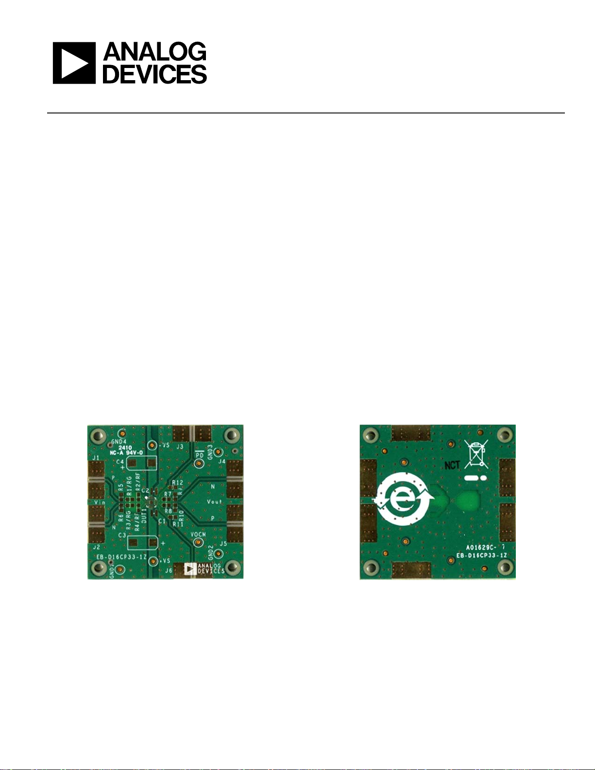
Figure 1. Component Side (LFCSP)
PLEASE SEE THE LAST PAGE FOR AN IMPORTANT
WARNING AND LEGAL TERMS AND CONDITIONS.
08990-003
Rev. 0 | Page 1 of 8
Figure 2. Circuit Side (LFCSP)
08990-003
Page 2

UG-132 Evaluation Board User Guide
TABLE OF CONTENTS
Features .............................................................................................. 1
General Description ......................................................................... 1
Revision History ............................................................................... 2
Differential Driver Evaluation Board Schematic .......................... 3
Evaluation Board Hardware ............................................................ 4
Power Supplies .............................................................................. 4
Feedback Networks and Input/Output Terminations ............. 4
REVISION HISTORY
10/10—Revision 0: Initial Version
V
Input ......................................................................................4
OCM
Common-Mode Voltage ...............................................................4
SMA Input/Output Connectors ..................................................4
Evaluation Board Layout ..................................................................5
Ordering Information .......................................................................6
Bill of Materials ..............................................................................6
Related Links ......................................................................................6
Rev. 0 | Page 2 of 8
Page 3

Evaluation Board User Guide UG-132
–V
S–VS
–V
S
+V
S
+V
S
+V
S
+V
S
+FB
–IN
+IN
–FB
V
OCM
+OUT
–OUT
PD
–V
S
E-PAD
+V
S
–V
S
VOCM
5 6 7 8
9
10
11
12
131415
1
16
2
3
4
17
DUT1
J2
J1
J6
J5
J4
J3
GND1
GND2
GND3
GND4
R6*
R3/RG*
R5*
R10*
R1/RG*
R7*
R8*
R2/RF*
R4/RF*
R11*
C4*
+
C2*
C3*
+
C1*
R12*
R9*
*USER DEFINE D V ALUE.
08990-001
PD
DIFFERENTIAL DRIVER EVALUATION BOARD SCHEMATIC
Figure 3. Differential Driver Evaluation Board Schematic
Rev. 0 | Page 3 of 8
Page 4

UG-132 Evaluation Board User Guide
EVALUATION BOARD HARDWARE
V
INPUT
POWER SUPPLIES
Power is applied to the board through test pins +VS and −VS
(see Figure 3). The board accommodates single or dual supplies.
For single-supply operation, connect the negative supply to the
ground plane.
It is very important that the power supply pins of the device
under test (DUT) have broadband decoupling circuitry. The
board layout facilitates this with footprints for a 0508 ceramic
capacitor C1 and C2) on each supply. Bulk decoupling is
provided by C3 and C4; 10 µF tantalum capacitors are
recommended.
FEEDBACK NETWORKS AND INPUT/OUTPUT TERMINATIONS
R1/RG and R2/RF comprise the upper resistive feedback loop
(see Figure 3), and R3/RG and R4/RF compose the lower
feedback loop. To minimize summing node capacitances, the
ground plane under and around Pin 1 and Pin 8 of the DUT
(see Figure 3) and the copper that connects to them have been
removed.
R5 and R6 are included as input termination resistors for applications that have single-ended inputs.
OCM
An external voltage can be applied to V
the ground plane of the board). In ADC driving applications, it
is convenient to apply the ADC dc reference voltage output
directly to J6. The R11 component position can be used for
both resistors and capacitors. A 0.1 μF capacitor is used in
normal applications to provide bypassing for the dc voltage
applied to the V
It is also possible to drive the V
source. In this case, omit R11 or reduce it to a value that allows
the desired signal to be passed.
OCM
pin.
input from an external ac
OCM
via J6 (referenced to
OCM
COMMON-MODE VOLTAGE
The internal common-mode feedback loop used in the differential drivers forces the output common-mode voltage to be equal
to the voltage applied to the V
excellent output balance.
input, thereby providing
OCM
SMA INPUT/OUTPUT CONNECTORS
The inputs and outputs have edge-mounted SMA connectors
for convenient connection to coaxial cables. The recommended
connector type is Johnson Components™, Part Number 1420701-801 or equivalent.
Rev. 0 | Page 4 of 8
Page 5

Evaluation Board User Guide UG-132
08990-004
08990-005
08990-006
EVALUATION BOARD LAYOUT
Figure 4. Assembly Drawing Component Side
Figure 5. Component Side Metallization (LFCSP)
Figure 6. Circuit Side Metallization (LFCSP)
Rev. 0 | Page 5 of 8
Page 6

UG-132 Evaluation Board User Guide
ORDERING INFORMATION
BILL OF MATERIALS
Table 1.
Qty Reference Designator Package Description
2 C3, C4 C7343 10 µF capacitor
2 C1, C2 C0508 Capacitor, 0.1uF
6 J1 to J6 SMASMT SMA connector
12 R1/RG, R2/RF, R3/RG, R4/RF, R5 to R12 R0603 Resistor, user defined value
8 +VS, −VS, PD/DIS, V
1 DUT1 16-lead LFCSP Device under test
1 PC board
RELATED LINKS
Table 2.
Resource Description
ADA4927-1 Product page, ultralow distortion current feedback differential ADC driver
ADA4930-1 Product page, ultralow noise driver for low voltage ADCs
ADA4932-1 Product page, low power differential ADC driver
ADA4937-1 Product page, single supply ultralow distortion differential ADC driver
ADA4938-1 Product page, ultralow distortion differential ADC driver
ADA4939-1 Product page, G > 2 ultralow distortion differential ADC driver
, GND1 to GND4 TP1 Test point
OCM
Rev. 0 | Page 6 of 8
 Loading...