Page 1

Evaluation Board User Guide
One Technology Way • P. O . Box 9106 • Norwood, MA 02062-9106, U.S.A. • Tel : 781.329.4700 • Fax : 781.461.3113 • www.analog.com
UG-071
Setting Up the Evaluation Board for the ADCLK846
PACKAGE LIST
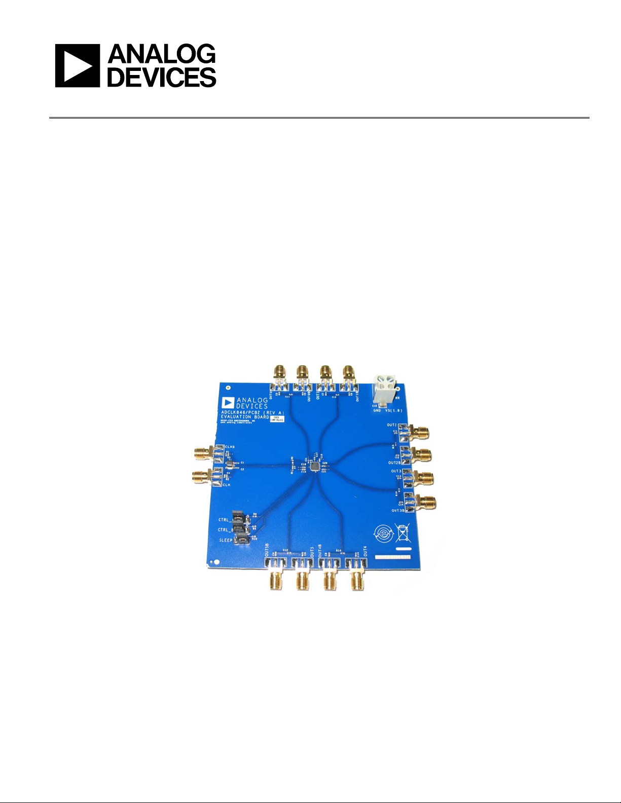
Evaluation board with components installed
Applicable documents (schematic and layout)
GENERAL DESCRIPTION
This user guide describes how to set up and use the evaluation
board for ADCLK846. The ADCLK846 data sheet contains full
technical details about the specifications and operation of this
device and should be consulted when using the evaluation board.
The ADCLK846 is a high performance clock fanout buffer.
The evaluation board is fabricated using a high quality Rogers®
dielectric material. Transmission line paths are kept as close to
100 Ω differentially as possible.
Figure 1. Evaluation Board
Please see the last page for an important warning and disclaimers. Rev. 0 | Page 1 of 8
08670-001
Page 2

UG-071 Evaluation Board User Guide
TABLE OF CONTENTS
Package List ....................................................................................... 1
General Description ......................................................................... 1
Revision History ............................................................................... 2
Recommended Board Setup ............................................................ 3
REVISION HISTORY
12/09—Revision 0: Initial Version
Clock Outputs ................................................................................4
Evaluation Board Schematics and Artwork ...................................5
ESD Caution...................................................................................8
Rev. 0 | Page 2 of 8
Page 3

Evaluation Board User Guide UG-071
RECOMMENDED BOARD SETUP
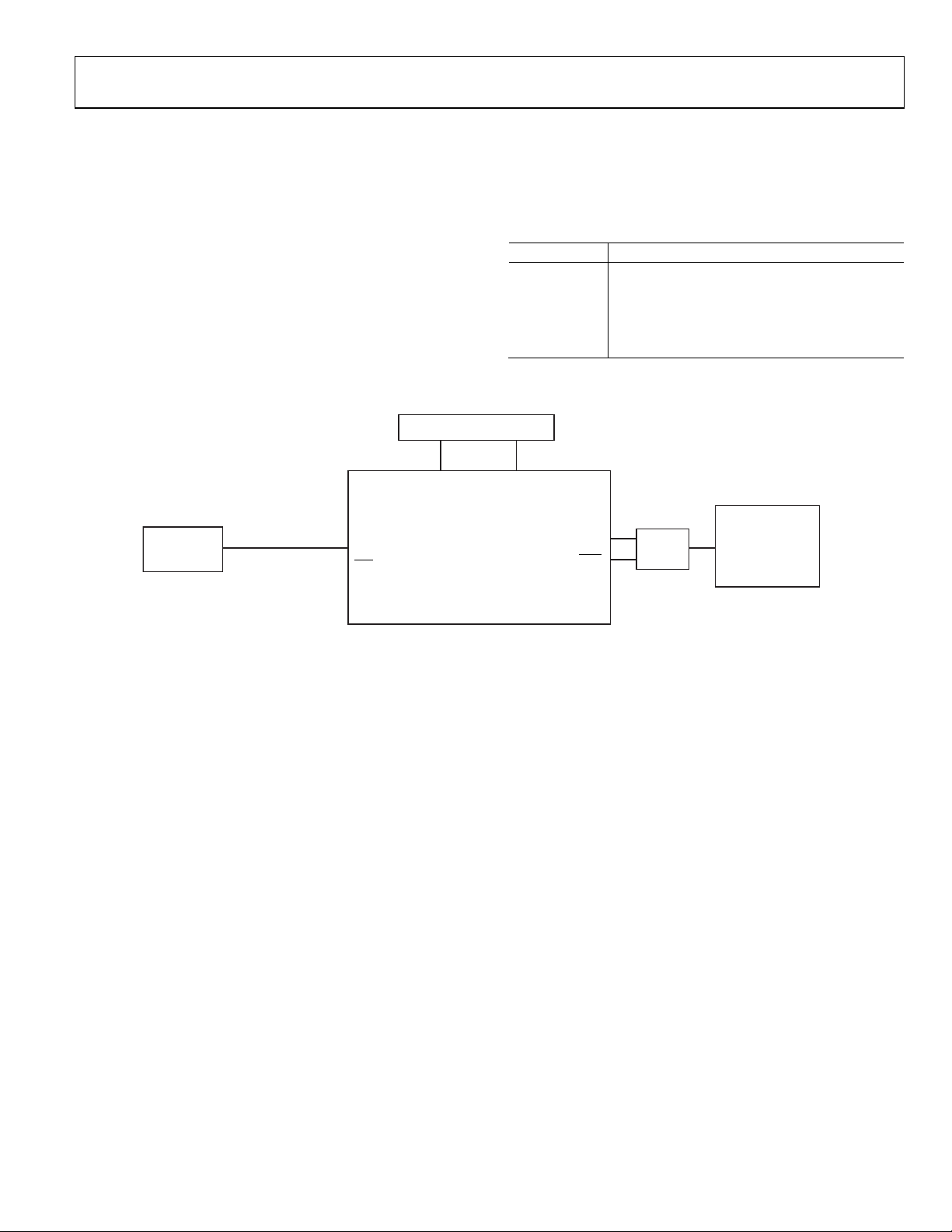
The recommended setup for the ADCLK846 evaluation board
is shown in Figure 2. V
is set to 1.8 V.
S
The CLK input is set up for single-ended-to-differential
operation via the balun on the evaluation board. In addition,
series capacitors (C3 and C4) in the path provide ac-coupled
inputs to the ADCLK846.
POWER SUPPLY
1.8V GND
The range of the peak-to-peak input voltage swing at CLK is
0.15 V to 1.8 V. Output jitter performance is degraded by input
slew rate, as shown in the ADCLK846 data sheet.
Table 1. Basic Equipment Required
Quantity Description
1 Single power supply
1 Signal source
1 High bandwidth oscilloscope
1 High bandwidth differential probe
2 Matched high speed cables
BOARD
GND
OUTx
OUTx
PROBE
OSCILLOSCOPE
08670-002
CLOCK
SOURCE
V
S
CLK
CLK
Figure 2. Recommended Setup for ADCLK846 Evaluation
ADCLK846
EVALUATION
Rev. 0 | Page 3 of 8
Page 4

UG-071 Evaluation Board User Guide
CLOCK OUTPUTS
The ADCLK846 outputs are pin programmable up to 6
differential LVDS outputs or 12 single-ended 1.8 V CMOS
outputs. Jumpers CTRL_A, CTRL_B, and SLEEP are used
to configure the outputs. See Ta ble 2 and Figure 3 for jumper
assignments.
For high precision measurements, it is recommended to evaluate
the nonlaunched outputs on the evaluation board. The nonlaunched
outputs do not go to the SMA connectors. In this case, the
ADCLK846 is physically close to the output load and avoids
the issues of driving a 50 Ω cable. CMOS is not designed to
operate in a 50 Ω environment.
The nonlaunched outputs have a full output swing with 100 Ω
differential trace impedance into a 100 Ω resistor to minimize
reflections. These outputs are set up to evaluate using a high
bandwidth differential probe and oscilloscope. See the
evaluation board schematic in Figure 4 for more details.
Outputs that go to a SMA connector may not have a full output
swing, and reflections may be observed.
Table 2. Output Pin Assignment
Jumper
Name Jumper Setting Affected Outputs
CTRL_A Logic 0 = LVDS; Logic 1 = CMOS Output 0 to Output 1
CTRL_B Logic 0 = LVDS; Logic 1 = CMOS Output 2 to Output 5
SLEEP Logic 1 = sleep Output 0 to Output 5
LVDS/CMOS
LVDS/CMOS
OUT0 (OUT0A)
OUT0 (OUT0B)
OUT1 (OUT1A)
OUT1 (OUT1B)
OUT2 (OUT2A)
OUT2 (OUT2B)
OUT3 (OUT3A)
OUT3 (OUT3B)
OUT4 (OUT4A)
OUT4 (OUT4B)
OUT5 (OUT5A)
OUT5 (OUT5B)
8670-003
V
REF
CLK
CLK
CTRL_A
CTRL_B
SLEEP
ADCLK846
Figure 3. 1:6 Clock/Data Buffer Block Diagram
Rev. 0 | Page 4 of 8
Page 5

Evaluation Board User Guide UG-071
EVALUATION BOARD SCHEMATICS AND ARTWORK
0.1UF
C20
0.1UF
GND
0.1UF
08670-004
PWR
1
C17
0.1UF
BYPASS CAPACITORS (DUT)
C15
4253
GNDGND
C9
0.1UF
1
C7
C5
4253
R11
OUT0
100
1
0.1UF
10UF
GND
GND
C16
OUT2B
3
GND
1
1
C12
16
OUT2
VS
19
20
VS
100OHM DIFF MATCH
22
OUT0
24
3
2
R6
VREF
R5
53
0.1UF
ADCLK846
VS
DNI
49.9
2
OUT3
4
GND
GND
53
C13
0.1UF
100OHM DIFF MATCH
0.1UF
1
53
14
CTRL_A
5
VS
CTRL_B
OUT4
12
OUT4B
10
8
SLEEP
7
GND
R9
GND
VS
31231
100OHM DIFF MATCH
100OHM DIFF MATCH
1.1K
SLEEP
OUT4
0.1UF
4253
GNDGND
C8
1
C6
R12
100
42
C4
100OHM DIFF MATCH
C2
C1
0.1UF
T1
1243
0
DNI
CLKB
0
R4
PRI
0
GND
GND
GND
DNI
53
1
Figure 4. Evaluation Board Schematic
Rev. 0 | Page 5 of 8
Page 6

UG-071 Evaluation Board User Guide
Figure 5. Top Trace Layer
08670-006
8670-007
Figure 6. Ground Plane Layer
Rev. 0 | Page 6 of 8
Page 7

Evaluation Board User Guide UG-071
8670-008
Figure 7. V
Power Plane Layer
S
08670-010
Figure 8. Bottom Trace Layer
Rev. 0 | Page 7 of 8
Page 8

UG-071 Evaluation Board User Guide
NOTES
ESD CAUTION
Evaluation boards are only intended for device evaluation and not for production purposes. Evaluation boards are supplied “as is” and without warranties of any kind, express,
implied, or statutory including, but not limited to, any implied warranty of merchantability or fitness for a particular purpose. No license is granted by implication or otherwise under
any patents or other intellectual property by application or use of evaluation boards. Information furnished by Analog Devices is believed to be accurate and reliable. However, no
responsibility is assumed by Analog Devices for its use, nor for any infringements of patents or other rights of third parties that may result from its use. Analog Devices reserves the
right to change devices or specifications at any time without notice. Trademarks and registered trademarks are the property of their respective owners. Evaluation boards are not
authorized to be used in life support devices or systems.
©2009 Analog Devices, Inc. All rights reserved. Trademarks and
registered trademarks are the property of their respective owners.
UG08670-0-12/09(0)
Rev. 0 | Page 8 of 8
 Loading...