

Page 1
5706
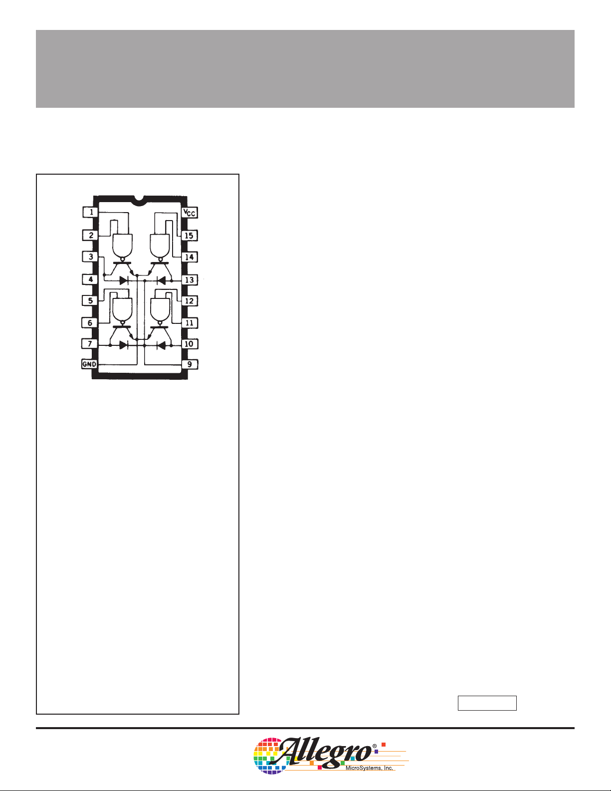
QUAD PERIPHERAL/POWER DRIVER
5706
QUAD 2-INPUT PERIPHERAL/POWER DRIVER
—TRANSIENT-PROTECTED OUTPUTS
This 16-lead quad 2-input peripheral/power driver is a bipolar
monolithic integrated circuit containing logic gates, high-current
switching transistors, and transient-suppression diodes on the same
chip. The four output transistors are capable of simultaneously sinking
300 mA continuously at ambient temperatures of up to +70°C. In the
OFF state, this driver will withstand at least 80 V.
The UDQ5706A quad driver is ideally suited for interface between
low-level or high-level logic and high-current/high-voltage loads.
Typical applications include driving peripheral loads such as incandescent lamps, light-emitting diodes, memories, and heaters.
The integral transient-suppression diodes allow its use with
inductive loads such as relays, solenoids, or stepping motors without
the need of discrete diodes.
Data Sheet
29306.1C
This device is furnished in a 16-pin DIP package with a copper
leadframe for improved thermal characteristics.
Dwg. No. A-9866
ABSOLUTE MAXIMUM RATINGS
at T
= +25°C
A
Supply Voltage, VCC.............................7.0 V
Input Voltage, V
Output Off-State Voltage,
V
................................................80 V
OFF
Output On-State Sink Current,
ION............................................. 600 mA
Suppression Diode Off-StateVoltage,
V
................................................80 V
OFF
Suppression Diode On-State Current,
DISCONTINUED PRODUCT
I
............................................. 600 mA
ON
Power Dissipation, P
Each Driver...................................0.8 W
Operating Free-Air Temperature Range,
.................................. -40°C to +85°C
T
A
Storage Temperature Range,
T
................................ -55°C to +150°C
S
...................................30 V
IN
........................ 2.0 W*
D
— FOR REFERENCE ONLY
FEATURES
■ DTL/TTL/PMOS/CMOS Compatible Inputs
■ Low Input Current
■ 300 mA Continuous Output Current
■ Standoff Voltage of 80 V
*Derate at the rate of 16.7 mW/°C above
TA = +25°C
Always order by complete part number, e.g., UDQ5706A .
Page 2
5706
QUAD PERIPHERAL/POWER DRIVER
RECOMMENDED OPERATING CONDITIONS
Min. Nom. Max. Units
Supply Voltage (VCC) 4. 75 5.0 5.25 V
Operating Temperature Range -40 +25 +85 °C
Current into any output (ON state) — — 300 mA
Dwg. No. A-7878A
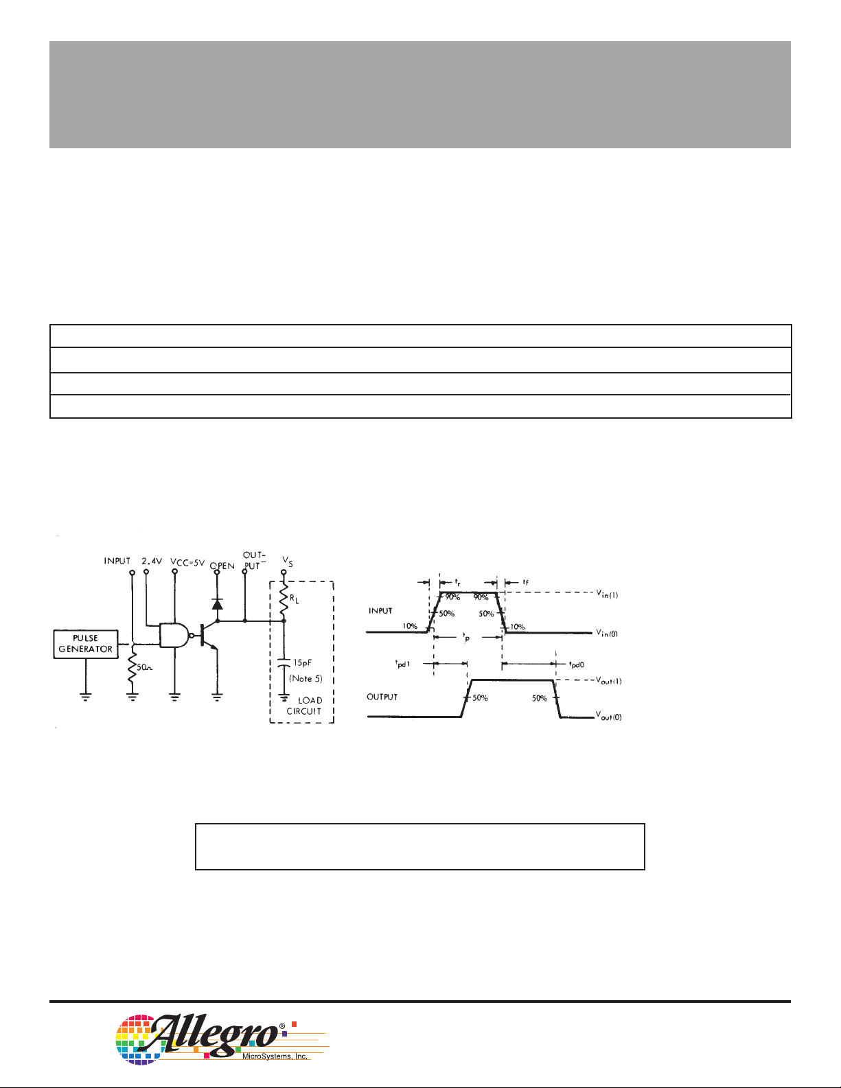
INPUT TEST PULSE CHARACTERISTICS
V
= 0 V t
IN(0)
= 3.5 V t
V
IN(1)
115 Northeast Cutoff, Box 15036
115 Northeast Cutoff, Box 15036
Worcester, Massachusetts 01615-0036 (508) 853-5000
Worcester, Massachusetts 01615-0036 (508) 853-5000
Copyright © 1995, 1996 Allegro MicroSystems, Inc.
= 7 ns tp = 1µs
f
= 14 ns PRR = 500 kHz
r
Dwg. No. A-7628C
Page 3

5706
QUAD PERIPHERAL/POWER DRIVER
ELECTRICAL CHARACTERISTICS over operating temperature range
(unless otherwise noted).
Test Conditions Limits
Driven Other
Characteristic Symbol Temp. V
“1” Output Reverse Current l
OFF
— MIN 2.0 V 2.0 V 80 V — — 100 µA—
— OPEN 2.0 V 2.0 V 80 V — — 100 µA—
CC
Input Input Output Min. Typ. Max. Units Notes
“0” Output Voltage V
“1” Input Voltage V
“0” Input Voltage V
“0” Input Current I
“1” Input Current I
Input Clamp Voltage V
Diode Leakage Current I
Diode Forward Voltage Drop V
“1” Level Supply Current l
“0” Level Supply Current l
ON
IN(1)
IN(0)
IN(0)
IN(1)
LK
R
F
CC(1)
CC(0)
SWITCHING CHARACTERISTICS at VCC = 5.0 V, T
— MIN 0.8 V V
— MIN 0.8 V V
150 mA — 0.35 0.5 V —
CC
300 mA — 0.5 0.7 V —
CC
— MIN — — — 2.0 — — V —
— MIN — — — — — 0.8 V —
— MAX 0.4 V 30 V — — -50 -100 µA 2
— MAX 30 V 0 V — — — 10 µA 2
— MIN -12 mA — — — — -1.5 V —
NOM NOM 0 V 0 V OPEN — — 200 µA3
NOM NOM V
CC
V
CC
— — 1.5 1.75 V 4
NOM MAX 5.0 V 5.0 V — — 16 24 mA 5
NOM MAX 0 V 0 V — — 70 98 mA 5
= 25°C
A
Limits
Characteristic Symbol Test Conditions Min. Typ. Max. Units Notes
Turn-on Delay Time t
Turn-off Delay Time t
pd0
pd1
VS = 70 V, RL = 465 Ω (10 Watts), — 200 — ns
C
= 15 pF (including probe and test fixture)
L
VS = 70 V, RL = 465 Ω (10 Watts), — 300 — ns
CL = 15 pF (including probe and test fixture)
NOTES: 1. Typical values are at VCC = 5.0 V, TA = 25°C.
2. Each input tested separately.
3. Diode leakage current measured at VR = V
4. Diode forward voltage drop measured at IF = 300 mA.
5. Per package.
off (min)
.
Page 4

5706
QUAD PERIPHERAL/POWER DRIVER
0.280
0.240
0.210
MAX
0.015
MIN
16
1
0.070
0.045
16
0.022
0.014
Dimensions in Inches
9
8
0.775
0.100
BSC
0.735
Dimensions in Millimeters
(Based on 1” = 25.4 mm)
9
0.005
MIN
0.150
0.115
0.014
0.008
0.355
0.204
0.430
MAX
0.300
BSC
Dwg. MA-001-16A in
7.11
6.10
1
1.77
1.15
5.33
MAX
0.39
MIN
0.558
0.356
NOTES: 1. Lead thickness is measured at seating
plane or below.
2. Lead spacing tolerance is non-cumulative.
3. Exact body and lead configuration at
vendor’s option within limits shown.
10.92
MAX
7.62
BSC
8
0.13
MIN
19.68
2.54
BSC
18.67
3.81
2.93
Dwg. MA-001-16A mm
Allegro MicroSystems, Inc. reserves the right to make, from time to time, such departures from
the detail specifications as may be required to permit improvements in the design of its products.
Components made under military approvals will be in accordance with the approval requirements.
The information included herein is believed to be accurate and reliable. However, Allegro
MicroSystems, Inc. assumes no responsibility for its use; nor for any infringements of patents or
other rights of third parties which may result from its use.
115 Northeast Cutoff, Box 15036
Worcester, Massachusetts 01615-0036 (508) 853-5000
 Loading...