

Page 1
Recommended for high-side switching applications that benefit from
separate logic and load grounds, these devices encompass load supply
voltages to 80 V and output currents to -500 mA. These 8-channel source
drivers are useful for interfacing between low-level logic and high-current
loads. Typical loads include relays, solenoids, lamps, stepper and/or servo
motors, print hammers, and LEDs.
All devices may be used with 5 V logic systems — TTL, Schottky TTL,
DTL, and 5 V CMOS. The UDN2981A, UDN2982A, UDN2982LW, and
A2982SLW are electrically interchangeable, will withstand a maximum
output off voltage of 50 V, and operate to a minimum of 5 V; the UDN2983A,
UDN2984A, UDN2984LW, and A2984SLW drivers are electrically interchangeable, will withstand an output voltage of 80 V, and operate to a
minimum of 35 V. All devices in this series integrate input current limiting
resistors and output transient suppression diodes, and are activated by an
active high input.
The suffix ‘A’ (all devices) indicates an 18-lead plastic dual in-line
package with copper lead frame for optimum power dissipation. Under
normal operating conditions, these devices will sustain 120 mA continuously
for each of the eight outputs at an ambient temperature of +50°C and a supply
of 15 V.
The suffix ‘LW’ (UDN2982LW and UDN2984LW only) indicates an 18lead surface-mountable wide-body SOIC package; the A2982SLW and
A2984SLW are provided in a 20-lead wide-body SOIC package with improved thermal characteristics.
The UDN2982A, UDN2982LW, A2982SLW, UDN2984A,
UDN2984LW, and A2984SLW drivers are also available for operation over
an extended temperature range to -40°C. To order, change the prefix ‘UDN’
to ‘UDQ’ or the suffix ‘SLW’ to ‘ELW’.
FEATURES
■ TTL, DTL, PMOS, or CMOS Compatible Inputs
■ 500 mA Output Source Current Capability
■ Transient-Protected Outputs
■ Output Breakdown Voltage to 80 V
■ DIP or SOIC Packaging
8-CHANNEL SOURCE DRIVERS
Always order by complete part number, e.g., UDN2981A .
Note that all devices are not available in all package styles.
ABSOLUTE MAXIMUM RATINGS
at 25°C Free-Air Temperature
Output Voltage Range, V
CE
(UDN2981A, UDN2982A,
UDN2982LW, and A2982SLW)
. . 5 V to 50 V
(UDN2983A, UDN2984A,
UDN2984LW, and A2984SLW) .
35 V to 80 V
Input Voltage, V
IN
(UDN2981A and UDN2983A) . . . . . . . . .
15 V
(UDN2982A, UDN2984A,
UDN2982LW, UDN2984LW,
A2982SLW, and A2984SLW) . . . . . . . . .
20 V
Output Current, I
OUT
. . . . . . . . . . . . . . -500 mA
Package Power Dissipation,
PD . . . . . . . . . . . . . . . . . . . . . . . See Graph
Operating Temperature Range,
T
A
. . . . . . . . . . . . . . . . . . . . -20°C to +85°C
Storage Temperature Range,
T
S
. . . . . . . . . . . . . . . . . . . -55°C to +150°C
Data Sheet
29310D*
1
2
3
4
5
6
7
8
V
S
GND
11
12
13
14
15
16
17
18
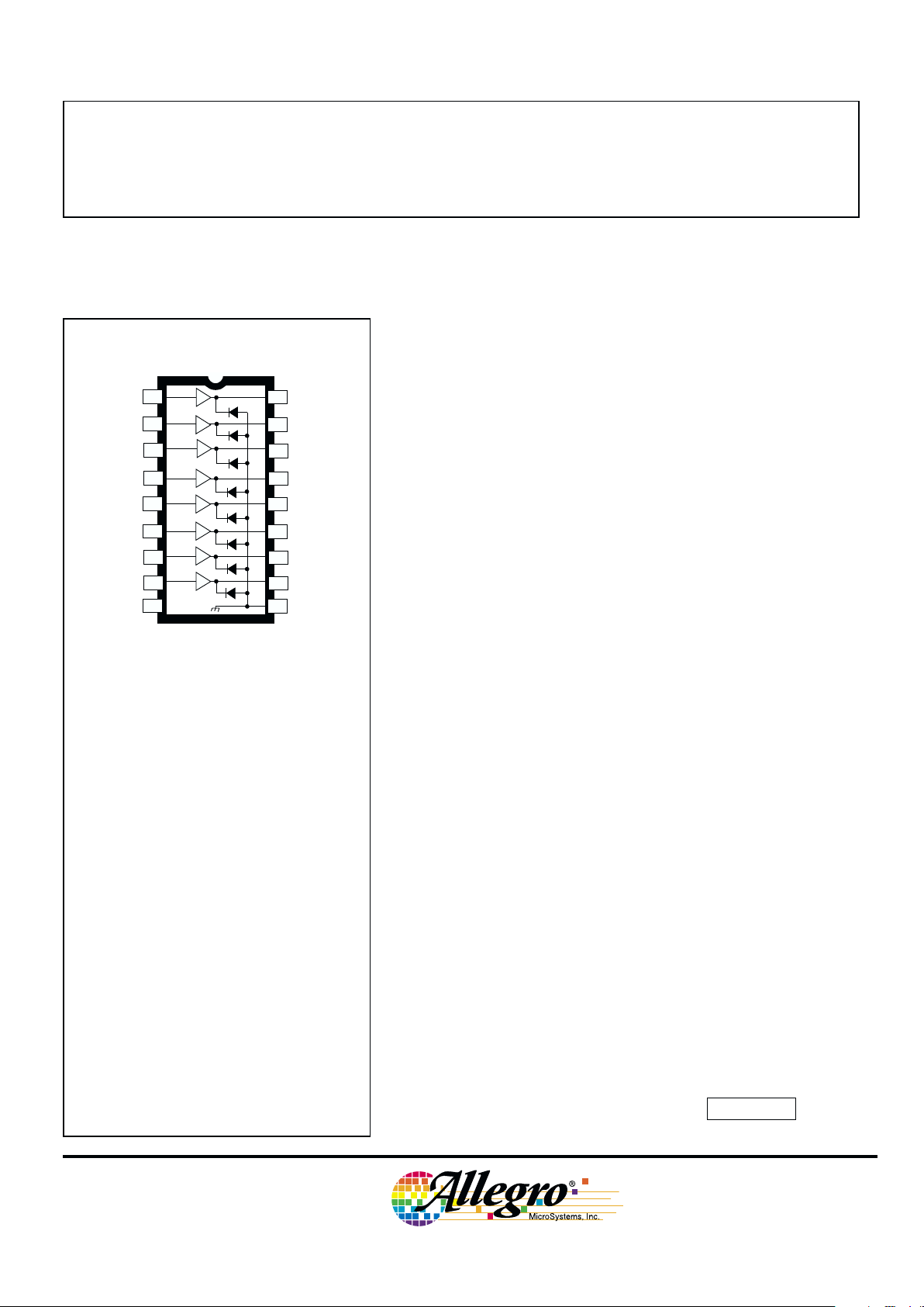
UDN2981A thru UDN2984A
Dwg. No. A-10, 243
2981
THRU
2984
Note that the UDN2980A series (dual in-line
package) and UDN2980LW series (small-outline
IC package) are electrically identical and share a
common terminal number assignment.
Page 2
2981
THRU
2984
8-CHANNEL
SOURCE DRIVERS
115 Northeast Cutoff, Box 15036
Worcester, Massachusetts 01615-0036 (508) 853-5000
2
A2982SLW and A2984SLW
13
14
15
16
17
19
12
18
20
11
NO
CONNECTION
1
2
3
8
9
4
5
6
7
10
NO
CONNECTION
NC
NC
Dwg. PP-064-2
GROUND+V
S
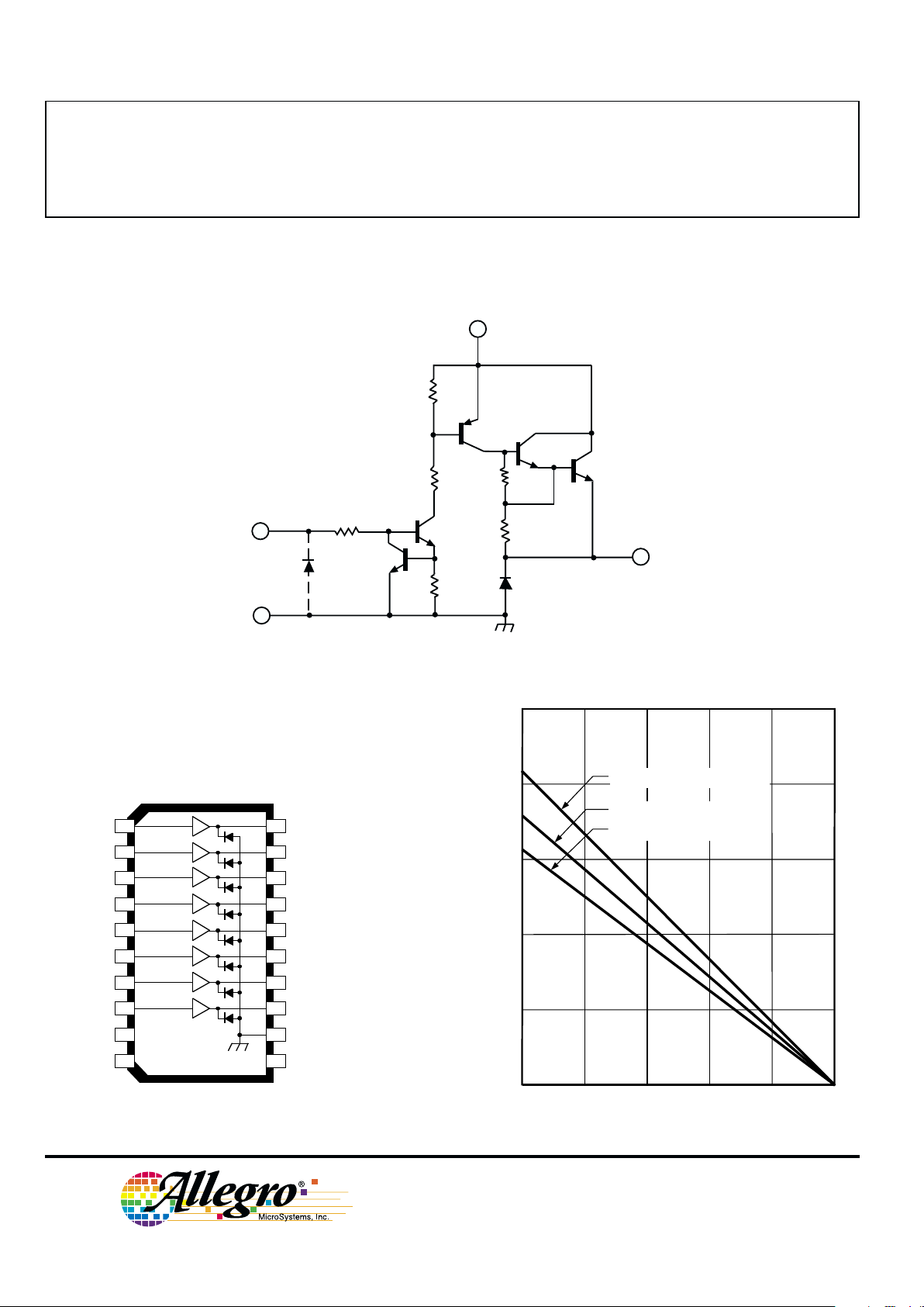
50 75 100 125 150
2.5
0.5
0
ALLOWABLE PACKAGE POWER DISSIPATION IN WATTS
AMBIENT TEMPERATURE IN °C
2.0
1.5
1.0
25
Dwg. GP-022-4
18-LEAD SOIC, R
θJA
= 80°C/W
20-LEAD SOIC, R
θJA
= 70°C/W
18-PIN DIP, R
θJA
= 60°C/W
One of Eight Drivers
OUTPUT
7.2 K
3 K
20 K
V
5
1.5 K
2983/84 ONLY
INPUT
GROUND
9
Dwg. No. A-10,242B
W
Copyright © 1977, 2000 Allegro MicroSystems, Inc.
Page 3
2981
THRU
2984
8-CHANNEL
SOURCE DRIVERS
www.allegromicro.com
3
Applicable Test Limits
Characteristic Symbol Devices Test Conditions Fig. Min. Typ. Max. Units
Output Leakage Current I
CEX
2981/82† VIN = 0.4 V*, VS = 50 V, TA = +70°C 1 — — 200 µA
2983/84† V
IN
= 0.4 V*, VS = 80 V, TA = +70°C 1 — — 200 µA
Output Sustaining V
CE(SUS)
2981/82† I
OUT
= -45 mA — 35 — — V
Voltage 2983/84† I
OUT
= -70 mA — 45 — — V
Collector-Emitter V
IN
= 2.4 V, I
OUT
= -100 mA 2 — 1.6 1.8 V
Saturation Voltage V
CE(SAT)
All VIN = 2.4 V, I
OUT
= -225 mA 2 — 1.7 1.9 V
V
IN
= 2.4 V, I
OUT
= -350 mA 2 — 1.8 2.0 V
Input Current 2981/83A VIN = 2.4 V 3 — 140 200 µA
I
IN(ON)
VIN = 3.85 V 3 — 310 450 µA
2982/84† V
IN
= 2.4 V 3 — 140 200 µA
VIN = 12 V 3 — 1.25 1.93 mA
Output Source Current l
OUT
2981/83A VIN = 2.4 V, VCE = 2.0 V 2 -350 — — mA
(Outputs Open) 2982/84† V
IN
= 2.4 V, VCE = 2.0 V 2 -350 — — mA
Supply Current I
S
2981/82† VIN = 2.4 V*, VS = 50 V 4 — — 10 mA
Leakage Current 2983/84† V
IN
= 2.4 V*, VS = 80 V 4 — — 10 mA
Clamp Diode I
R
2981/82† VR = 50 V, VIN = 0.4 V* 5 — — 50 µA
Forward Voltage 2983/84† VR = 80 V, VIN = 0.4 V* 5 — — 50 µA
Clamp Diode V
F
All IF = 350 mA 6 — 1.5 2.0 V
Turn-On Delay t
ON
All 0.5 EIN to 0.5 E
OUT
, RL = 100Ω, — — 1.0 2.0 µs
V
S
= 35 V
Turn-Off Delay t
OFF
All 0.5 EIN to 0.5 E
OUT
, RL = 100Ω, — — 5.0 10 µs
VS = 35 V, See Note
ELECTRICAL CHARACTERISTICS at TA = +25°C (unless otherwise specified).
NOTES: Turn-off delay is influenced by load conditions. Systems applications well below the specified output loading may require
timing considerations for some designs, i.e., multiplexed displays or when used in combination with sink drivers in a totem
pole configuration.
Negative current is defined as coming out of (sourcing) the specified device terminal.
* All inputs simultaneously.
† Complete part number includes a prefix (A or UDN) and a suffix (A or SLW) as follows:
UDN2981A,
UDN2982A, UDN2982LW, or A2982SLW,
UDN2983A,
UDN2984A, UDN2984LW, or A2984SLW.
Page 4

2981
THRU
2984
8-CHANNEL
SOURCE DRIVERS
115 Northeast Cutoff, Box 15036
Worcester, Massachusetts 01615-0036 (508) 853-5000
4
TEST FIGURES
Figure 1 Figure 2 Figure 3
Dwg. No. A-11,083 Dwg. No. A-11,084 Dwg. No. A-11,085
V
V
IN
CEX
I
S
µA
V
V
V
I
OUT
IN
CE
S
V
mA
OPEN
V
V
IN
IN
I
S
mA
Dwg. No. A-11,086 Dwg. No. A-11,087 Dwg. No. A-11,088
Figure 5 Figure 6
Figure 4
OPEN
OPEN
V
I
F
F
V
V
S
I
R
V
IN
µA
V
IN
I
S
S
V
OPEN
mA
Page 5

2981
THRU
2984
8-CHANNEL
SOURCE DRIVERS
www.allegromicro.com
5
Allowable peak collector current
as a function of duty cycle
Series UDN2980A
100
V = 35 V
8
7
6
4
5
NUMBER OF OUTPUTS
CONDUCTING
SIMULTANEOUSLY
90
80
70
60
50
40
30
20
10
0
0
50
100
150
200
250
300
350
400
450
500
RECOMMENDED MAXIMUM OUTPUT CURRENT
ALLOWABLE PEAK COLLECTOR CURRENT IN mA AT 50°C
PER CENT DUTY CYCLE
S
3
100
V = 35 V
8
7
6
4
5
NUMBER OF OUTPUTS
CONDUCTING
SIMULTANEOUSLY
90
80
70
60
50
40
30
20
10
0
0
50
100
150
200
250
300
350
400
450
500
RECOMMENDED MAXIMUM OUTPUT CURRENT
ALLOWABLE PEAK COLLECTOR CURRENT IN mA AT 70°C
PER CENT DUTY CYCLE
S
3
Dwg. No. A-11,111BDwg. No. A-11,106B
UDN2981A and UDN2982A
100
V = 15 V
8
7
6
4
5
NUMBER OF OUTPUTS
CONDUCTING
SIMULTANEOUSLY
90
80
70
60
50
40
30
20
10
0
0
50
100
150
200
250
300
350
400
450
500
RECOMMENDED MAXIMUM OUTPUT CURRENT
ALLOWABLE PEAK COLLECTOR CURRENT IN mA AT 50°C
PER CENT DUTY CYCLE
S
3
100
V = 15 V
8
7
6
4
5
NUMBER OF OUTPUTS
CONDUCTING
SIMULTANEOUSLY
90
80
70
60
50
40
30
20
10
0
0
50
100
150
200
250
300
350
400
450
500
RECOMMENDED MAXIMUM OUTPUT CURRENT
ALLOWABLE PEAK COLLECTOR CURRENT IN mA AT 70°C
PER CENT DUTY CYCLE
S
3
Dwg. No. A-11,107B
Dwg. No. A-11,108B
Page 6

2981
THRU
2984
8-CHANNEL
SOURCE DRIVERS
115 Northeast Cutoff, Box 15036
Worcester, Massachusetts 01615-0036 (508) 853-5000
6
100
8
7
6
4
5
NUMBER OF OUTPUTS
CONDUCTING
SIMULTANEOUSLY
90
80
70
60
50
40
30
20
10
0
0
50
100
150
200
250
300
350
400
450
500
RECOMMENDED MAXIMUM OUTPUT CURRENT
PER CENT DUTY CYCLE
3
V = 60 V
S
ALLOWABLE PEAK COLLECTOR CURRENT IN mA AT 70°C
Allowable peak collector current
as a function of duty cycle
UDN2983A and UDN2984A
Dwg. No. A-11,109B Dwg. No. A-11,110B
100
8
7
6
4
5
NUMBER OF OUTPUTS
CONDUCTING
SIMULTANEOUSLY
90
80
70
60
50
40
30
20
10
0
0
50
100
150
200
250
300
350
400
450
500
RECOMMENDED MAXIMUM OUTPUT CURRENT
PER CENT DUTY CYCLE
3
V = 60 V
S
ALLOWABLE PEAK COLLECTOR CURRENT IN mA AT 50°C
Input current as a function
of input voltage
Typical electrosensitive
printer application
TYPICAL
2.5
INPUT CURRENT, I (mA)
IN
2.0
1.5
1.0
0.5
2
4
6
8
10 12
INPUT VOLTAGE (VOLTS)
MAXIMUM
Dwg. No. A-11,115B
1
2
3
4
5
6
7
8
9
11
12
13
14
15
16
17
18
10
ELECTRODES
IN
1
IN
2
IN
3
IN
4
IN
5
IN
6
IN
7
IN
8
V
S
R
L
R
L
R
L
R
L
R
L
R
L
R
L
R
L
Dwg. No. A-11,113A
Page 7

2981
THRU
2984
8-CHANNEL
SOURCE DRIVERS
www.allegromicro.com
7
UDN2981A, UDN2982A, UDN2983A, and UDN2984A
Dimensions in Inches
(controlling dimensions)
Dimensions in Millimeters
(for reference only)
0.014
0.008
0.300
BSC
Dwg. MA-001-18A in
0.430
MAX
18
1
9
0.280
0.240
0.210
MAX
0.070
0.045
0.015
MIN
0.022
0.014
0.100
BSC
0.005
MIN
0.150
0.115
10
0.920
0.880
NOTES: 1. Exact body and lead configuration at vendor’s option within limits shown.
2. Lead spacing tolerance is non-cumulative.
3. Lead thickness is measured at seating plane or below.
4. Supplied in standard sticks/tubes of 21 devices.
0.355
0.204
7.62
BSC
Dwg. MA-001-18A mm
10.92
MAX
18
1
9
7.11
6.10
5.33
MAX
1.77
1.15
0.39
MIN
0.558
0.356
2.54
BSC
0.13
MIN
3.81
2.93
10
23.37
22.35
Page 8

2981
THRU
2984
8-CHANNEL
SOURCE DRIVERS
115 Northeast Cutoff, Box 15036
Worcester, Massachusetts 01615-0036 (508) 853-5000
8
UDN2982LW and UDN2984LW
(add “TR” to part number for tape and reel)
Dimensions in Inches
(for reference only)
Dimensions in Millimeters
(controlling dimensions)
0° TO 8°
1 2
3
0.020
0.013
0.0040
MIN.
0.0125
0.0091
0.050
0.016
D
wg. MA-008-18A in
0.050
BSC
18 10
0.419
0.394
0.2992
0.2914
0.4625
0.4469
0.0926
0.1043
NOTES: 1. Exact body and lead configuration at vendor’s option within limits shown.
2. Lead spacing tolerance is non-cumetive.
3. Supplied in standard sticks/tubes of 41 devices or
add “TR” to part number for tape and reel.
0° TO 8°
1
18
2
3
0.51
0.33
0.10
MIN.
0.32
0.23
1.27
0.40
Dwg. MA-008-18A mm
1.27
BSC
10
7.60
7.40
10.65
10.00
11.75
11.35
2.65
2.35
Page 9

2981
THRU
2984
8-CHANNEL
SOURCE DRIVERS
www.allegromicro.com
9
A2982SLW and A2984SLW
(add “TR” to part number for tape and reel)
Dimensions in Inches
(for reference only)
Dimensions in Millimeters
(controlling dimensions)
0° TO 8°
1 2
3
0.020
0.013
0.0040
MIN.
0.0125
0.0091
0.050
0.016
Dwg. MA-008-20 in
0.050
BSC
20 11
0.2992
0.2914
0.419
0.394
0.5118
0.4961
0.0926
0.1043
NOTES: 1. Exact body and lead configuration at vendor’s option within limits shown.
2. Lead spacing tolerance is non-cumulative.
3. Supplied in standard sticks/tubes of 37 devices or
add “TR” to part number for tape and reel.
0° TO 8°
1
20
2
3
0.51
0.33
0.10
MIN.
Dwg. MA-008-20 mm
1.27
BSC
11
0.32
0.23
1.27
0.40
7.60
7.40
10.65
10.00
13.00
12.60
2.65
2.35
Page 10

2981
THRU
2984
8-CHANNEL
SOURCE DRIVERS
115 Northeast Cutoff, Box 15036
Worcester, Massachusetts 01615-0036 (508) 853-5000
10
POWER SOURCE DRIVERS
IN ORDER OF 1) OUTPUT CURRENT, 2) OUTPUT VOLTAGE, 3) NUMBER OF DRIVERS
Output Ratings *
Features
Serial Latched Diode Saturated Internal
mA V # Input Drivers Clamp Outputs Protection Part Number
†
-25 60 8 – X – – – 5815
60 10 X X active pull-down – – 5810-F and 6809/10
60 12 X X active pull-down – – 5811 and 6811
60 20 X X active pull-down – – 5812-F and 6812
60 32 X X active pull-down – – 5818-F and 6818
85 8 – – – – – 6118
-120 -25 8 – – X X – 2585
30 8 – – X X – 2985
50 8 X X X X – 5895
-350 35 8 – – X – X 2987
50 8 – – X – – 2981 and 2982
50 8 X X X – – 5891
-50 8 – – X – – 2580
80 8 – – X – – 2983 and 2984
80 8 X X X – – 5890
-80 8 – – X – – 2588
-500 6 1 – – – MOSFET X 2525 and 2535
6 2 – – – MOSFET X 2526 and 2536
-4000 60 4 – – X – – 2944
* Current is maximum specified test condition, voltage is maximum rating. See specification for sustaining voltage limits or
over-current protection voltage limits.
† Complete part number includes additional characters to indicate operating temperature range and package style.
The products described here are manufactured under one or more U.S. patents or U.S.
patents pending.
Allegro MicroSystems, Inc. reserves the right to make, from time to time, such departures
from the detail specifications as may be required to permit improvements in the performance,
reliability, or manufacturability of its products. Before placing an order, the user is cautioned
to verify that the information being relied upon is current.
Allegro products are not authorized for use as critical components in life-support devices or
systems without express written approval.
The information included herein is believed to be accurate and reliable. However, Allegro
MicroSystems, Inc. assumes no responsibility for its use; nor for any infringement of patents or
other rights of third parties which may result from its use.
 Loading...