

Page 1
2596
8-CHANNEL
AND
2597
2596
SATURATED SINK DRIVERS
2597
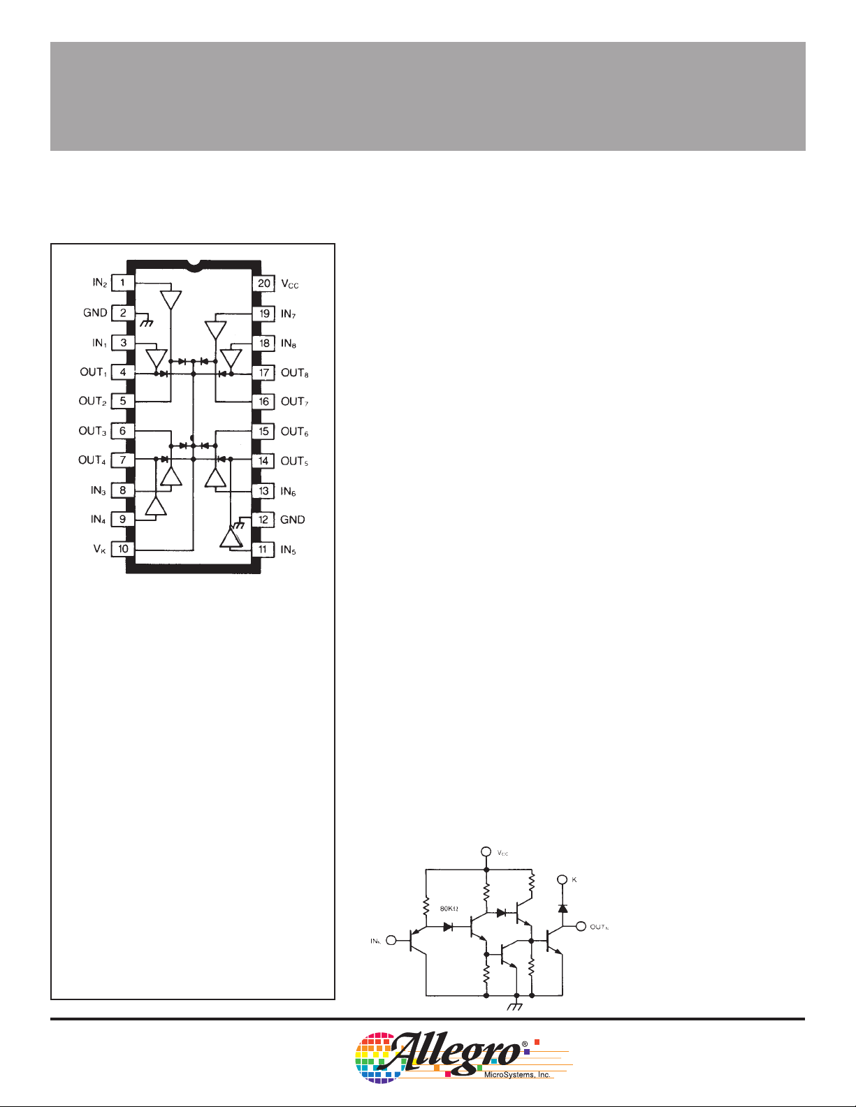
by UDN2596A and UDN2597A sink driver ICs. These devices can be
used as interface buffers between standard low-power digital logic
(particularly MOS) and high-power loads such as relays, solenoids,
stepping motors, and LED or incandescent displays. The eight saturated sink drivers in each device feature high-voltage, high-current
open-collector outputs. Transient suppression clamp diodes and a
minimum 35 V output sustaining voltage allow their use with many
inductive loads.
emitter voltage drops as well as improved turn-off times due to an
active pull-down function within the output predrive section. The
UDN2596A is for use with output loads to 500 mA while the
UDN2597A is for use with loads to 1 A. Adjacent outputs may be
paralleled for higher load currents.
AND
8-CHANNEL
SATURATED SINK DRIVERS
Low output-saturation voltages at high load currents are provided
The saturated (non-Darlington) NPN outputs provide low collector-
Data Sheet
29320.2B
Dwg. No. W-100
ABSOLUTE MAXIMUM RATINGS
at T
= + 25°C
A
OutputVoltage,VCE................................ 50 V
Output Current, I
(UDN2596A) ............................ 500 mA
(UDN2597A) ................................ 1.0 A
Supply Voltage, V
Input Voltage, V
Package Power Dissipation,
P
............................................. 2.27 W*
D
Operating Temperature Range,
T
................................. -20°C to +85°C
A
Storage Temperature Range,
TS.............................. - 65°C to +150°C
*Derate at the rate of 18.2 mW/°C above
T
= +25°C
A
OUT
............................ 7.0 V
CC
................................. 7.0 V
lN
Inputs require very low input current and are activated by a low
logic level consistent with the much greater sinking capability associated with NMOS, CMOS, and TTL logic. The UDN2596A and
UDN2597A are rated for use with 5 V logic levels.
Both devices are furnished in 20-pin DIP packages with copper
leadframes for improved thermal characteristics. The UDN2596A is
also available for operation between -40°C and +85°C. To order,
change the prefix from ‘UDN’ to ‘UDQ’.
FEATURES
■ Non-Inverting Function
■ Low Output ON Voltages
■ Up to 1.0 A Sink Capability
■ 50 V Min. Output Breakdown
■ Output Transient-Suppression
Diodes
■ Output Pull-Down for
Fast Turn-Off
■ TTL, CMOS Compatible Inputs
■ Automotive Capable
ONE OF EIGHT DRIVERS
Dwg. No. W-101
Page 2
2596
AND
2597
8-CHANNEL
SATURATED SINK DRIVERS
ELECTRICAL CHARACTERISTICS at T
Characteristics Symbol Devices Test Conditions Min. Max. Units
Output Leakage Current I
Output Sustaining Voltage V
Output Saturation Voltage V
Clamp Diode Leakage Current I
Clamp Diode Forward Voltage V
Logic lnput Current I
Supply Current I
CEX
CE(sus)
CE(SAT)
R
F
lN(0)
I
lN(1)
CC(ON)
= +25°C, V
A
Applicable
Both V
UDN2596A l
UDN2597A l
UDN2596A l
UDN2597A l
Both VR = 50 V — 10 µA
UDN2596A IF = 300 mA — 1.8 V
UDN2597A IF = 750 mA — 1.8 V
UDN2956A VIN = 0.8 V — -15 µA
UDN2597A VIN = 0.8 V — -50 µA
Both VIN = 2.4 V — 10 µA
UDN2596A any one driver VIN = 0.8 V — 6.0 mA
UDN2597A any one driver VIN = 0.8 V — 31 mA
= 5.0 V
CC
Limits
= 50 V, VIN = 2.4 V — 10 µA
OUT
= 300 mA, L = 2 mH 35 — V
OUT
= 750 mA, L = 2 mH 35 — V
OUT
= 300 mA — 0.5 V
OUT
= 750 mA — 1.0 V
OUT
Turn-On Delay t
Turn-Off Delay t
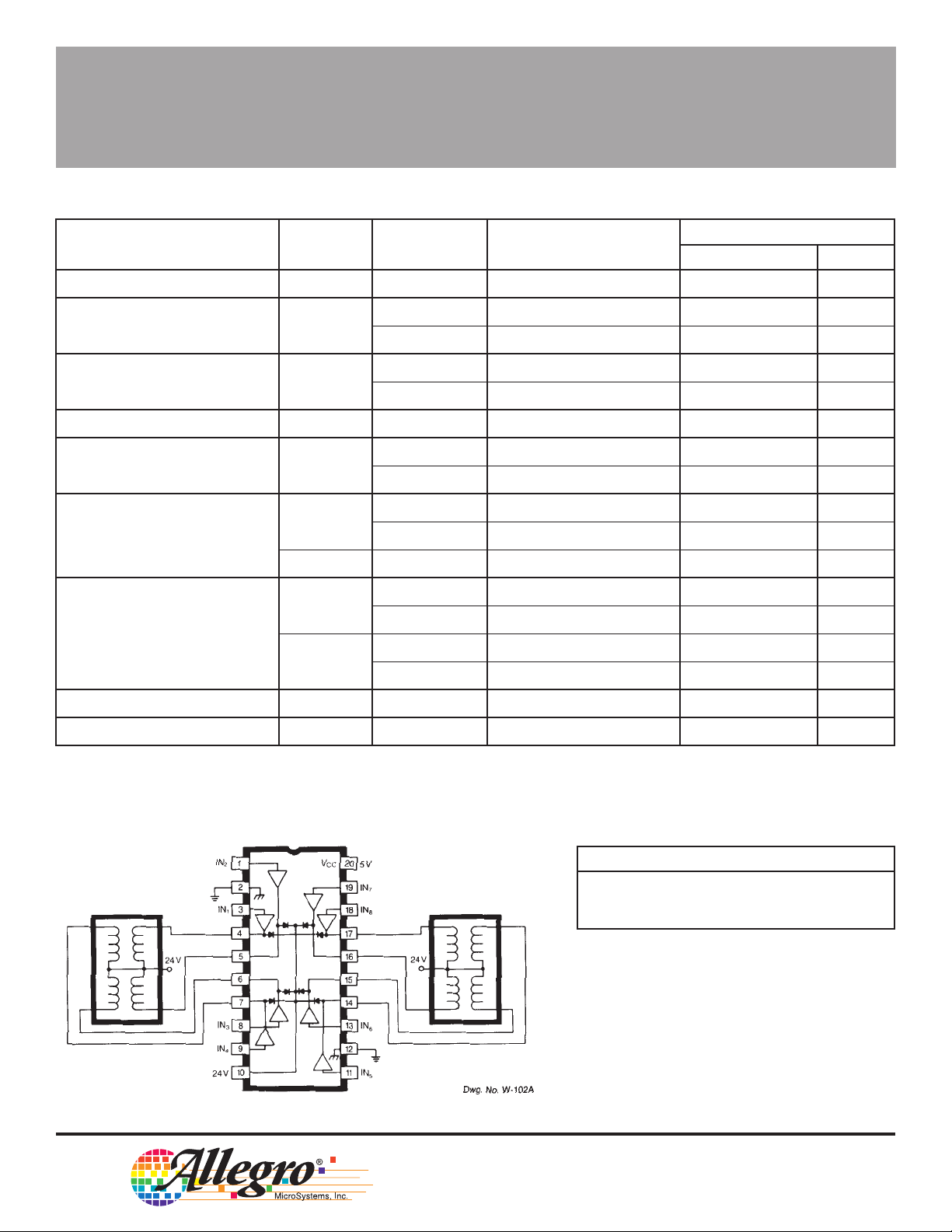
TYPICAL APPLICATION
DUAL STEPPER MOTOR DRIVE
I
CC(OFF)
pd0
pd1
UDN2596A all drivers VIN = 2.4 V 0.75 1.3 mA
UDN2597A all drivers VIN = 2.4 V 0.75 15 mA
Both 0.5 EIN to 0.5 E
Both 0.5 EIN to 0.5 E
OUT
OUT
— 3.0 µs
— 2.0 µs
RECOMMENDED
OPERATING CONDITIONS
Type Number Logic I
UDN2596A 5.0 V 300 mA
UDN2597A 5.0 V 750 mA
Note: Pins 2 and 12 must both be connected to
power ground.
OUT
115 Northeast Cutoff, Box 15036
Worcester, Massachusetts 01615-0036 (508) 853-5000
Copyright © 1984, 1999, Allegro MicroSystems, Inc.
Page 3

2596
AND
2597
8-CHANNEL
SATURATED SINK DRIVERS
Dimensions in Inches
(controlling dimensions)
20
0.280
0.240
11
0.014
0.008
0.300
BSC
0.430
MAX
0.210
MAX
7.11
6.10
0.015
MIN
20
1
0.070
0.045
1.060
0.100
BSC
10
0.005
MIN
0.980
0.150
0.115
0.022
0.014
Dwg. MA-001-20 in
Dimensions in Millimeters
(for reference only)
0.355
11
1
1.77
1.15
26.92
2.54
BSC
10
0.13
MIN
24.89
0.204
7.62
BSC
10.92
MAX
5.33
MAX
0.39
MIN
0.558
0.356
NOTES: 1. Exact body and lead configuration at vendor’s option within limits shown.
2. Lead spacing tolerance is non-cumulative.
3. Lead thickness is measured at seating plane or below.
3.81
2.93
Allegro MicroSystems, Inc. reserves the
right to make, from time to time, such
departures from the detail specifications as may
be required to permit improvements in the
design of its products.
The information included herein is believed
to be accurate and reliable. However, Allegro
MicroSystems, Inc. assumes no responsibility
for its use; nor for any infringements of patents
or other rights of third parties which may result
from its use.
Dwg. MA-001-20 mm
Page 4

2596
AND
2597
8-CHANNEL
SATURATED SINK DRIVERS
POWER SINK DRIVERS
SELECTION GUIDE
IN ORDER OF 1) OUTPUT CURRENT, 2) OUTPUT VOLTAGE, 3) NUMBER OF DRIVERS
Output Ratings *
Serial Latched Diode Saturated Internal
Features
mA V # Input Drivers Clamp Outputs Protection Part Number
100 20 8 – – – X – 2595
30 32 X X – – – 5833
40 32 X X – X – 5832
250 135 7 – – X – – 7003
300 45 1 Hall Sensor/Driver X – X 5140
50 7 – – X – – 2003
50 8 – – X – – 2803
50 8 – – X X – 2596
60 2 Hall Sensor/Driver – X – 5275
60 4 – – X X X 2557
95 7 – – X – – 2023
95 8 – – X – – 2823
350 50 4 – X X – – 5800
50 7 – – X – – 2004
50 8 – – X – – 2804
50 8 – X X – – 5801
50 8 X X – – – 5821
80 8 X X – – – 5822
50 8 X X X – – 5841
80 8 X X X – – 5842
95 7 – – X – – 2024
95 8 – – X – – 2824
450 30 28 Dual 4 to 14-Line Decoder/Driver – – 6817
600 60 4 – – – X X 2547
60 4 – – X X X 2549
700 60 4 – – X X X 2543 and 2559
750 50 8 – – X X – 2597
900 14 2 Hall Sensor/Driver X X X 3625
26 2 Hall Sensor/Driver X X X 3626
1000 46 4 Stepper Motor Controller/Driver MOS – 7024 and 7029
1200 46 4 Microstepping Controller/Driver MOS – 7042
1250 50 4 Stepper Motor Translator/Driver – X 5804
50 4 – – X – – 2064 and 2068
1500 80 4 – – X – – 2065 and 2069
1600 50 9 X X – – X 5829
1800 50 4 – – X – – 2544
50 4 – – X – – 2540
3000 46 4 Stepper Motor Controller/Driver MOS – 7026
46 4 Microstepping Controller/Driver MOS – 7044
4000 50 4 – – X – – 2878
80 4 – – X – – 2879
* Current is maximum specified test condition, voltage is maximum rating. See specification for sustaining voltage limits or
over-current protection voltage limits.
† Complete part number includes additional characters to indicate operating temperature range and package style.
†
115 Northeast Cutoff, Box 15036
Worcester, Massachusetts 01615-0036 (508) 853-5000
 Loading...