

Page 1
2547
PROTECTED
QUAD POWER DRIVERS
Providing interface between low-level logic and power loads, the
UDK/UDN/UDQ2547B and UDK/UDN/UDQ2547EB quad power
drivers combine logic gates and high-current bipolar outputs with
complete output protection. Each of the four outputs will sink 600 mA
in the ON state. The outputs have a minimum breakdown voltage
(load dump) of 60 V and a sustaining voltage of 40 V. The inputs are
compatible with TTL and 5 V CMOS logic systems and include internal
pull-down resistors to ensure that the outputs remain OFF if the inputs
are open-circuited.
Over-current protection for each channel has been designed into
these devices and is activated at approximately 1.3 A. It protects each
output from short circuits with supply voltages up to 25 V. When a
maximum driver output current is reached, that output drive is reduced
linearly, maintaining a constant load current. If the over-current or
short circuit condition continues, each channel has an independent
thermal limit circuit which will sense the rise in junction temperature
and turn OFF the individual channel that is at fault. Foldback circuitry
decreases the output current if excessive voltage is present across the
output and assists in keeping the device within its SOA (safe operating
area).
Each output also includes diagnostics for increased device protection. If any output is shorted or opened, the diagnostics can signal the
controlling circuitry through a common FAULT pin.
These devices can be used to drive various resistive loads including incandescent lamps (without warming or limiting resistors). With
the addition of external output clamp diodes, they can be used to drive
inductive loads such as relays, solenoids, or dc stepping motors.
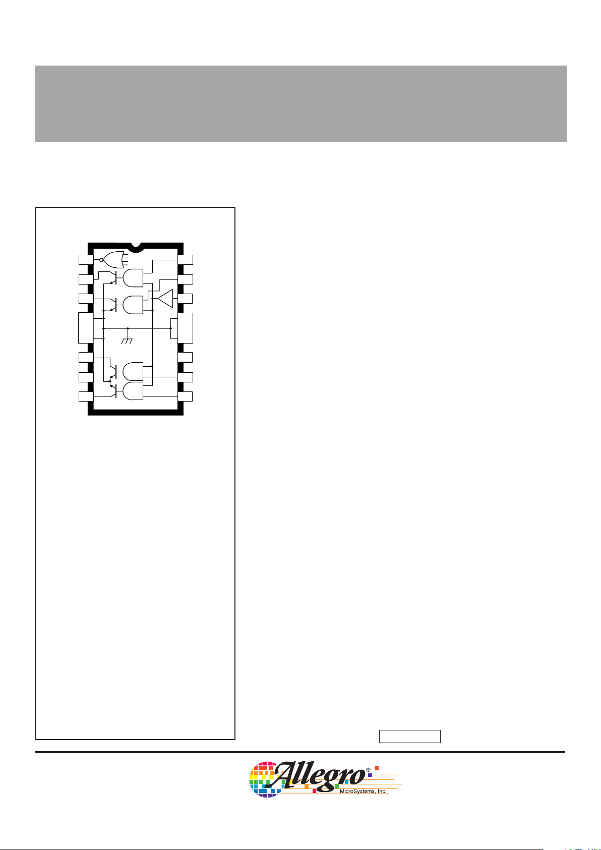
The suffix ‘B’ devices are 16-pin power DIPs while the suffix ‘EB’
devices are 28-lead power PLCCs for surface-mount applications.
Both packages are of batwing construction to provide for maximum
package power dissipation.
UDx2547B
2547
PROTECTED
QUAD POWER DRIVERS
ABSOLUTE MAXIMUM RATINGS
at T
A
= 25°C
Output Voltage, V
OUT
............................ 60 V
Over-Current Protected Output Voltage,
V
OUT
............................................... 25 V
Output Current, I
OUT
.......................... 1.3 A*
FAULT Output Voltage, V
F
................... 40 V
Supply Voltage, V
CC
............................ 7.0 V
Input Voltage, V
IN
or VEN...................... 7.0 V
Package Power Dissipation,
P
D
........................................ See Graph
Operating Temperature Range, T
A
Prefix ‘UDK’ ............... -40°C to +125°C
Prefix ‘UDN’ ................. -20
°C to +85°C
Prefix ‘UDQ’................. -40
°C to +85°C
Storage Temperature Range,
T
S
............................... -55°C to +150°C
*Outputs are current limited at approximately
1.3 A per driver and junction temperature limited
if current in excess of 1.3 A is attempted. See
Circuit Description and Application for further
information.
Always order by complete part number: a prefix to indicate operating temperature range + the basic four-digit part number + a suffix to
indicate package style, e.g., UDK2547EB .
FEATURES
■ Output SOA Protection ■ Low Output-Saturation Voltage
■ Diagnostic FAULT Output ■ TTL and 5 V CMOS Compatible Inputs
■ Independent Over-Current Protection for Each Driver
■ Independent Thermal Protection for Each Driver
■ 600 mA Output Current per Channel
Data Sheet
29317.4C
1
2
3
14
4
5
6
7
89
10
11
12
13
15
16
ENABLE
GROUND
GROUND
OUT
3
NO
CONNECT.
GROUND
GROUND
OUT
2
OUT
1
FAULT
OUT
4
V
CC
IN
4
Dwg. PP-018A
IN
1
IN
2
IN
3
SUPPLY
Page 2
2547
PROTECTED
QUAD POWER DRIVERS
115 Northeast Cutoff, Box 15036
Worcester, Massachusetts 01615-0036 (508) 853-5000
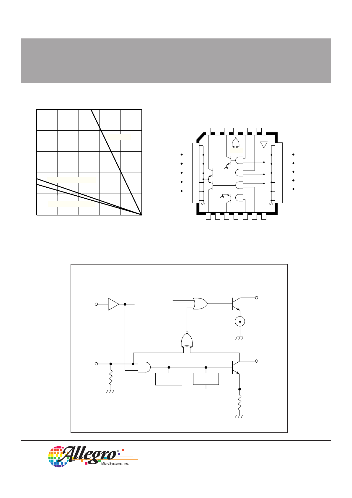
UDx2547EB
FUNCTIONAL BLOCK DIAGRAM
<<1 Ω
OUT
Dwg. FP-007
N
FAULT
COMMON CONTROL
ONE OF FOUR DRIVERS
ABLE
IN
N
CURRENT
LIMIT
THERMAL
SHUTDOWN
1
2
3
4
5
6
7
8
9
10
11
12
13
14
15
16
17
18
19
20
21
22
23
24
25
26
27
28
GROUND
GROUND
GROUND
GROUND
Dwg. PP-019
NO
CONNECTION
NC
ENABLE
SUPPLY
NC
CC
V
OUT
1
OUT
2
OUT
3
OUT
4
IN
4
IN
3
IN
2
IN
1
NO
CONNECTION
NO
CONNECTION
FAULT
NC
FAULT
W
Copyright © 1989, 1993, Allegro MicroSystems, Inc.
50 75 100 125 150
10
6
4
2
0
ALLOWABLE PACKAGE POWER DISSIPATION IN WATTS
TEMPERATURE IN °C
8
25
R = 6°C/W
θJT
Dwg. GP-004-1A
SUFFIX 'EB', R = 36°C/W
θJA
SUFFIX 'B', R = 43°C/W
θJA
Page 3
2547
PROTECTED
QUAD POWER DRIVERS
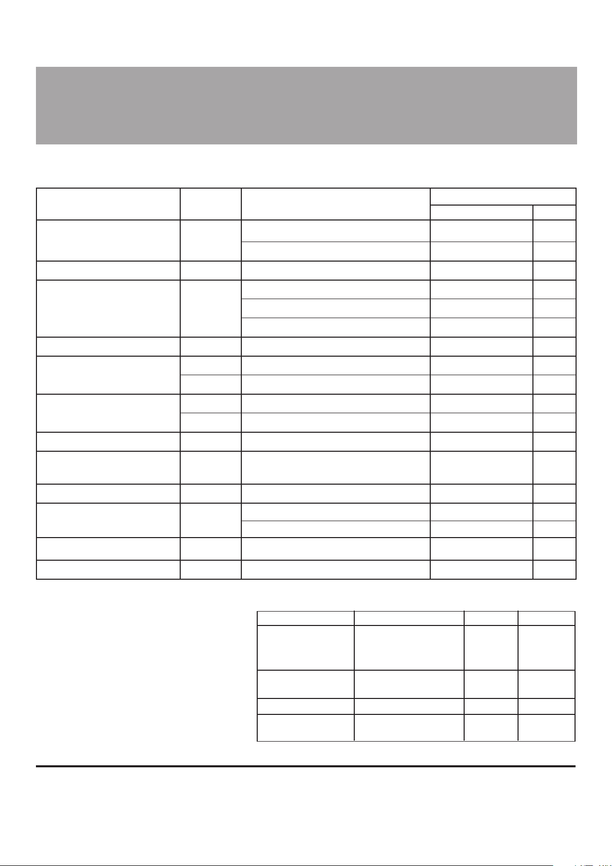
STATUS IN
N
ENABLE OUT
N
FAULT
Normal Load H H L H
LH HH
XL HH
Over-Current or
Short to Supply H H R L
Thermal Fault H H H L
Open Load or
Short to Ground L H L L
ELECTRICAL CHARACTERISTICS at T
A
= +25°C (prefix ‘UDN’) or over operating
temperature range (prefix ‘UDK’ or ‘UDQ’), V
CC
= 4.75 V to 5.5 V
Limits
Characteristic Symbol Test Conditions Min. Typ. Max. Units
Output Leakage Current* I
OUT
V
OUT
= 60 V, VIN = 0.8 V, VEN = 2.0 V — 30 150 µA
V
OUT
= 60 V, VIN = 2.0 V, VEN = 0.8 V — 30 150 µA
Output Sustaining Voltage V
OUT(SUS)
I
OUT
= 100 mA, V
IN
= 0.8 V, V
CC
= Open 40 — — V
Output Saturation Voltage V
OUT(SAT)
I
OUT
= 400 mA — — 300 mV
I
OUT
= 500 mA — — 400 mV
I
OUT
= 600 mA — — 550 mV
Over-Current Limit I
OUT
5 ms PulseTest, V
OUT
= 5.0 V — 1. 3 1.7 A
Input Voltage Logic 1 V
IN(1)
or V
EN(1)
2.0 — — V
Logic 0 V
lN(0)
or V
EN(0)
— — 0.8 V
Input Current Logic 1 V
IN(1)
or V
EN(1)
= 2.0 V — — 60 µA
Logic 0 V
IN(0)
or V
EN(0)
= 0.8 V 10 — — µA
Fault Output Leakage Current I
F
VF = 40 V — <1.0 2.0 µA
Fault Output Current I
F
VF = 40 V, Driver Outputs Open,
V
IN
= 0.8 V, V
EN
= 2.0 V 40 60 80 µA
Fault Output Saturation Voltage V
F(SAT)
IF = 30 µA — 0.1 0.4 V
Total Supply Current I
CC
All Outputs ON — 45 50 mA
All Outputs OFF — 6.0 10 mA
Thermal Shutdown T
J
— 165 — °C
Thermal Hysteresis ∆T
J
—15— °C
Typical Data is for design information only.
*Measurement includes XOR input current
and other elements.
X = Don’t care. R = Linear drive, current limited.
TRUTH TABLE
Page 4

2547
PROTECTED
QUAD POWER DRIVERS
115 Northeast Cutoff, Box 15036
Worcester, Massachusetts 01615-0036 (508) 853-5000
CIRCUIT DESCRIPTION AND APPLICATION
These devices monitor their outputs for open or shorted conditions.
Both conditions are sensed by comparing the input and output states.
Note that the FAULT output is operational only if the ENABLE input is
high. When a fault condition is sensed, the FAULT output will go to a
low state. An external FAULT output filter capacitor (0.1µF) is recommended to eliminate erroneous switching.
INCANDESCENT LAMP DRIVER
High incandescent lamp turn-ON/in-rush currents can contribute to
poor lamp reliability and destroy semiconductor lamp drivers.
Warming (parallel) or current-limiting (series) resistors protect both
driver and lamp but use significant power either when the lamp is OFF
or when the lamp is ON, respectively. Lamps with steady-state current
ratings up to 600 mA can be driven without the need for warming or
current-limiting resistors, if lamp turn-ON time is not a concern.
When an incandescent lamp is initially turned ON, the cold filament
is at minimum resistance and would normally allow a 10x to 12x in-rush
current. With these drivers, during turn-ON, the high in-rush current is
sensed by the internal low-value sense resistor, drive current to the
output stage is diverted by the shunting transistor, the output stage
operates in a linear mode, and the load current is limited to approximately 1.3 A. During lamp warmup, the filament resistance increases
to its maximum value, the output driver goes into saturation and applies
maximum rated voltage to the lamp.
INDUCTIVE LOAD DRIVER
With the addition of external clamp diodes, bifilar (unipolar)
stepper motors and other inductive loads can be driven directly.
The external diodes prevent damage to the output transistors by
suppressing the high-voltage spikes that occur when turning
OFF an inductive load. For rapid current decay (fast turn-OFF speeds),
the use of Zener diodes will raise the flyback voltage and improve
performance. However, the peak voltage must not exceed the specified minimum sustaining voltage (V
SUPPLY
+ VZ + VF ≤ V
OUT(SUS)
).
OVER-CURRENT CONDITIONS
In the event of a shorted load, or stalled motor, the load current
will attempt to increase. As described above, the drive current to the
affected output stage is linearly reduced (limiting the load current to
about 1.3 A), causing the output stage to go linear. As the junction
temperature of the output stage increases, the thermal shutdown circuit
will shut OFF the affected output. If the fault condition is corrected, the
output driver will return to its normal saturated condition.
NORMAL LAMP IN-RUSH CURRENT
TIME
Dwg. WP-005A
NOT TO SCALE
LAMP CURRENT
CURRENT LIMIT
THERMAL SHUTDOWN
THERMAL HYSTERESIS
SHORT CIRCUIT
Page 5

2547
PROTECTED
QUAD POWER DRIVERS
0.508
0.204
7.62
BSC
Dwg. MA-001-17A mm
10.92
MAX
16
1
8
7.11
6.10
5.33
MAX
1.77
1.15
0.39
MIN
0.558
0.356
2.54
BSC
0.13
MIN
3.81
2.93
9
19.68
18.67
NOTE 4
NOTES: 1. Exact body and lead configuration at vendor’s option within limits shown.
2. Lead spacing tolerance is non-cumulative
3. Lead thickness is measured at seating plane or below.
4. Webbed lead frame. Leads 4, 5, 12, and 13 are internally one piece.
UDN2547B and UDQ2547B
Dimensions in Inches
(controlling dimensions)
Dimensions in Millimeters
(for reference only)
0.020
0.008
0.300
BSC
Dwg. MA-001-17A in
0.430
MAX
16
1
8
0.280
0.240
0.210
MAX
0.070
0.045
0.015
MIN
0.022
0.014
0.100
BSC
0.005
MIN
0.150
0.115
9
0.775
0.735
NOTE 4
Page 6

2547
PROTECTED
QUAD POWER DRIVERS
115 Northeast Cutoff, Box 15036
Worcester, Massachusetts 01615-0036 (508) 853-5000
0.51
MIN
4.57
4.20
1.27
BSC
12.57
12.32
11.582
11.430
128
INDEX AREA
Dwg. MA-005-28A mm
0.812
0.661
0.331
0.533
12.57
12.32
26
25
19
18 12
11
4
5
11.58
11.43
5.56
4.85
5.56
4.85
UDN2547EB and UDQ2547EB
Dimensions in Inches
(controlling dimensions)
Dimensions in Millimeters
(for reference only)
NOTES: 1. Exact body and lead configuration at vendor’s option within limits shown.
2. Lead spacing tolerance is non-cumulative
3. Webbed lead frame. Leads 5 through 11 and 19 through 25 are internally one piece.
18 12
0.020
MIN
0.050
BSC
128
INDEX AREA
Dwg. MA-005-28A in
0.026
0.032
0.013
0.021
26
25
19
11
4
5
0.165
0.180
0.495
0.485
0.456
0.450
0.495
0.485
0.456
0.450
0.219
0.191
0.219
0.191
Page 7

2547
PROTECTED
QUAD POWER DRIVERS
Allegro MicroSystems, Inc. reserves the right to make, from time to time, such departures from
the detail specifications as may be required to permit improvements in the design of its products.
The information included herein is believed to be accurate and reliable. However, Allegro
MicroSystems, Inc. assumes no responsibility for its use; nor for any infringements of patents or
other rights of third parties which may result from its use.
Page 8

2547
PROTECTED
QUAD POWER DRIVERS
115 Northeast Cutoff, Box 15036
Worcester, Massachusetts 01615-0036 (508) 853-5000
POWER SINK DRIVERS
SELECTION GUIDE
IN ORDER OF 1) OUTPUT CURRENT, 2) OUTPUT VOLTAGE, 3) NUMBER OF DRIVERS
Output Ratings *
Features
Serial Latched Diode Saturated Internal
mA V # Input Drivers Clamp Outputs Protection Part Number
†
100 20 8 – – – X – 2595
30 32 X X – – – 5833
40 32 X X – X – 5832
250 135 7 – – X – – 7003
300 45 1 Hall Sensor/Driver X – X 5140
50 7 – – X – – 2003
50 8 – – X – – 2803
50 8 – – X X – 2596
60 2 Hall Sensor/Driver – X – 5275
60 4 – – X X X 2557
95 7 – – X – – 2023
95 8 – – X – – 2823
350 50 4 – X X – – 5800
50 7 – – X – – 2004
50 8 – – X – – 2804
50 8 – X X – – 5801
50 8 X X – – – 5821
80 8 X X – – – 5822
50 8 X X X – – 5841
80 8 X X X – – 5842
95 7 – – X – – 2024
95 8 – – X – – 2824
450 30 28 Dual 4 to 14-Line Decoder/Driver – – 6817
600 60 4 – – – X X 2547
60 4 – – X X X 2549
700 60 4 – – X X X 2543 and 2559
750 50 8 – – X X – 2597
900 14 2 Hall Sensor/Driver X X X 3625
26 2 Hall Sensor/Driver X X X 3626
1000 46 4 Stepper Motor Controller/Driver MOS – 7024 and 7029
1200 46 4 Microstepping Controller/Driver MOS – 7042
1250 50 4 Stepper Motor Translator/Driver – X 5804
50 4 – – X – – 2064 and 2068
1500 80 4 – – X – – 2065 and 2069
1600 50 9 X X – – X 5829
1800 50 4 – – X – – 2544
50 4 – – X – – 2540
3000 46 4 Stepper Motor Controller/Driver MOS – 7026
4000 50 4 – – X – – 2878
80 4 – – X – – 2879
* Current is maximum specified test condition, voltage is maximum rating. See specification for sustaining voltage limits or
over-current protection voltage limits.
† Complete part number includes additional characters to indicate operating temperature range and package style.
 Loading...