

Page 1
OUT
OUT
GROUND
GROUND
OUT
OUT
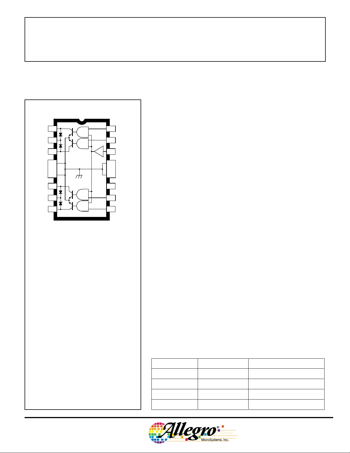
UDN/UDQ2543B
1
4
2
K
3
3
4
5
6
2
7
K
8
1
16
15
14
13
12
11
10
9
IN
4
IN
3
ENABLE
GROUND
GROUND
V
CC
IN
2
IN
1
2543
PROTECTED
QUAD POWER DRIVER
Providing interface between low-level logic and power loads to
100 W, the UDx2543B and UDx2543EB quad power drivers combine
AND logic gates and high-current bipolar outputs. Each of the four
independent outputs can sink up to 700 mA in the ON state. The
outputs have a minimum breakdown voltage (load dump) of 60 V and
a sustaining voltage of 35 V. The inputs are compatible with most
TTL, DTL, LSTTL, and 5 V CMOS and PMOS logic systems.
Over-current protection has been designed into each channel of
the UDx2543B/EB and typically occurs at 1 A. It protects any one
channel from output short circuits with supply voltages up to 25 V.
When the maximum output current is reached, that output stage is
driven linearly. If the over-current condition continues, that output’s
thermal limiting will operate, limiting that output’s power dissipation to
approximately 2.4 W. The outputs also include diodes for voltage
clamping with inductive loads such as relays, solenoids, or dc stepper
motors.
Data Sheet
29317.2B
Dwg. PP-017-1
ABSOLUTE MAXIMUM RATINGS
at TA = 25°C
Output Voltage, V
Over-Current Protected Output Voltage,
V
. . . . . . . . . . . . . . . . . . . . . . . 25 V
OUT
Output Current, I
Supply Voltage, V
Input Voltage, V
Package Power Dissipation,
P
. . . . . . . . . . . . . . . . . . . . See Graph
D
Operating Temperature Range, T
(UDN2543B/EB) . . . . -20°C to +85°C
(UDQ2543B/EB) . . . . -40
Storage Temperature Range,
T
. . . . . . . . . . . . . . . -55°C to +150°C
S
*Outputs are peak current limited at approximately 1.0 A per driver. See Circuit Description
and Applications for further information.
. . . . . . . . . . . . . 60 V
OUT
. . . . . . . . . . . . . 1.0 A*
OUT
. . . . . . . . . . . . . . 7.0 V
CC
or VEN. . . . . . . . . . 18 V
IN
A
°C to +85°C
These devices are supplied in a 16-pin power DIP of batwing
construction (suffix ‘B’) to provide for maximum package power dissipation. They are also available in a 28-lead PLCC (suffix ‘EB’) for
surface-mount applications. All devices are rated for continuous
operation over the temperature range of -20°C to +85°C (UDN2543B/
EB) or for use in automotive applications over an extended temperature range as the UDQ2543B/EB.
FEATURES
■ 700 mA Output Current per Channel
■ Low Output-Saturation Voltage
■ Integral Output Transient-Suppression Diodes
■ TTL, CMOS, PMOS, NMOS Compatible Inputs
■ Independent Over-Current Protection for Each Output
Always order by complete part number:
Part Number Package Operating Temperature
UDN2543B 16-Pin DIP -20°C to +85°C
UDN2543EB 28-Lead PLCC -20°C to +85°C
UDQ2543B 16-Pin DIP -40°C to +85°C
UDQ2543EB 28-Lead PLCC -40°C to +85°C
Page 2

2543
PROTECTED
QUAD POWER DRIVER
FUNCTIONAL BLOCK DIAGRAM
(1 OF 4 CHANNELS)
K
OUT
N
ENABLE
IN
V
CC
N
THERMAL
LIMIT
<<1 Ω
Dwg. FP-041
NOTE: These devices do not include an absolute thermal shutdown. Package power dissipation under fault conditions (2.4 W in the faulted
channel) must therefore be evaluated at maximum operating temperature.
UDN/UDQ2543EB
10
8
R = 6°C/W
θJT
6
4
SUFFIX 'EB', R = 36°C/W
θJA
2
SUFFIX 'B', R = 43°C/W
θJA
0
25
ALLOWABLE PACKAGE POWER DISSIPATION IN WATTS
50 75 100 125 150
TEMPERATURE IN °C
Dwg. GP-004-1A
115 Northeast Cutoff, Box 15036
Worcester, Massachusetts 01615-0036 (508) 853-5000
Copyright © 1986, 1993, Allegro MicroSystems, Inc.
GROUND
GROUND
2
OUT
4
5
6
7
8
9
10
11
12
3
OUT
1
OUT
K
2
3
14
13
4
K
OUT
NO
CONNECTION
1
NC
NC
15
NO
CONNECTION
1
2
IN
28
16
IN
ENABLE
IN
26
27
GROUND
25
24
23
22
21
20
19
GROUND
V
CC
18
17
3
4
IN
SUPPLY
Dwg. PP-019-1
Page 3
2543
PROTECTED
QUAD POWER DRIVER
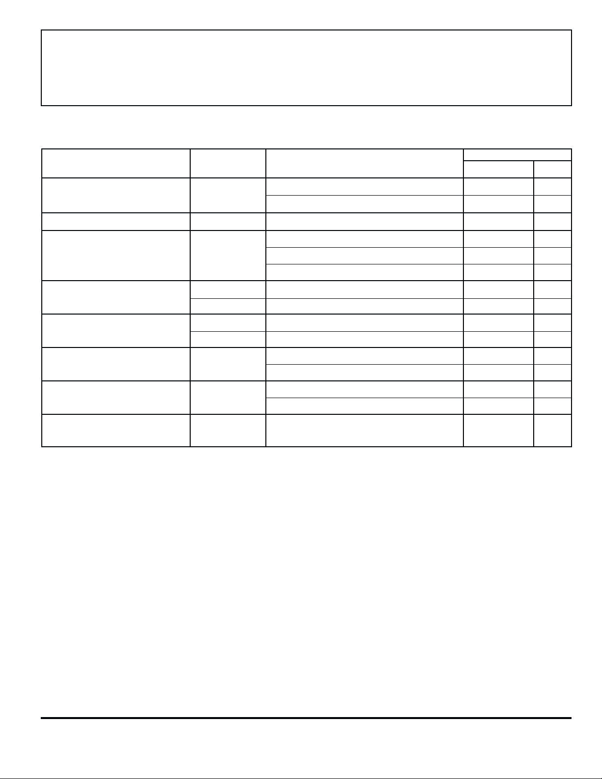
ELECTRICAL CHARACTERISTICS at T
= +25°C (UDN2543B/EB) or over operating
A
temperature range (UDQ2543B/EB only), VCC = 4.75 V to 5.25 V
Limits
Characteristic Symbol Test Conditions Min. Max. Units
Output Leakage Current I
Output Sustaining Voltage V
Output Saturation Voltage V
CEX
OUT(SUS)
OUT(SAT)
Input Voltage Logic 1 V
Logic 0 V
Input Current Logic 1 V
Logic 0 V
Total Supply Current I
Clamp Diode Forward Voltage V
Clamp Diode I
Leakage Current
CC
F
R
V
= 60 V, VIN = 0.8 V, VEN = 2.0 V — 100 µA
OUT
V
= 60 V, VIN = 2.0 V, VEN = 0.8 V — 100 µA
OUT
I
= 100 mA, VIN = VEN = 0.8 V 35 — V
OUT
I
= 100 mA, VIN = VEN = 2.0 V — 200 mV
OUT
I
= 400 mA, VIN = VEN = 2.0 V — 400 mV
OUT
I
= 700 mA, VIN = VEN = 2.0 V — 600 mV
OUT
or V
I
OUT
IN(1)
IN(0)
IN(1)
IN(0)
EN(1)
or V
EN(0)
or V
or V
= 2.0 V — 20 µA
EN(1)
= 0.8 V — -10 µA
EN(0)
= 700 mA*, V
Outputs Open, V
†
= VEN = 2.0 V — 65 mA
IN
†
= 0.8 V, VEN = 2.0 V — 15 mA
IN
2.0 — V
— 0.8 V
IF = 1.0 A — 1.6 V
I
= 1.5 A — 2.0 V
F
VR = 60 V, VIN = VEN = 2.0 V, — 50 µA
D
+ D2 or D3 + D
1
4
Negative current is defined as coming out of (sourcing) the specified terminal.
As used here, -100 is defined as greater than +10 (absolute magnitude convention) and the minimum is implicitly zero.
* Pulse test, allowable package power dissipation will be exceeded at increased ambient temperatures.
† All inputs simultaneously, all other tests are performed with each input tested separately.
Page 4

2543
PROTECTED
QUAD POWER DRIVER
TYPICAL OUTPUT BEHAVIOR
NOT TO SCALE
SHORT CIRCUIT
OUTPUT CURRENT
CURRENT LIMIT (12 V SUPPLY)
CURRENT LIMIT (24 V SUPPLY)
TIME
NORMAL LOAD
Dwg. WP-013-1
CIRCUIT DESCRIPTION AND APPLICATION
INCANDESCENT LAMP DRIVER
For incandescent lamp applications, the UDx2549B/EB or
UDx2559B/EB, with improved shortcircuit protection and thermal
limiting, are recommended.
INDUCTIVE LOAD DRIVER
Bifilar (unipolar) stepper motors, relays, or solenoids can be driven
directly. The internal flyback diodes prevent damage to the output
transistors by suppressing the high-voltage spikes that occur when
turning OFF an inductive load. For rapid current decay (fast turn-OFF
speeds), the use of Zener diodes will raise the flyback voltage and
improve performance. However, the peak voltage must not exceed the
specified minimum sustaining voltage (V
FAULT CONDITIONS
In the event of a shorted load, the load current will attempt to
increase. As described above, the drive current to the affected
output stage is diverted, causing the output stage to go linear, limiting
the peak output current to approximately 1 A. As the power dissipation
of that output stage increases, a thermal gradient sensing circuit will
become operational, further decreasing the drive current to the affected output stage and reducing the output current to a value dependent on supply voltage (I
OUT
≈ 2.4/V
SUPPLY
corrected, the output stage will return to its normal saturated condition.
+ VZ + VF ≤ V
SUPPLY
OUT(SUS)
). If the fault condition is
).
Due to the independent operation of the four channels, only
a single channel should be shorted at a time. Multiple overload
conditions may be tolerated provided rated package power
dissipation is not exceeded.
115 Northeast Cutoff, Box 15036
Worcester, Massachusetts 01615-0036 (508) 853-5000
Page 5

0.280
0.240
16
UDN2543B and UDQ2543B
Dimensions in Inches
(controlling dimensions)
NOTE 4
9
2543
PROTECTED
QUAD POWER DRIVER
0.020
0.008
0.430
MAX
0.300
BSC
0.210
MAX
7.11
6.10
0.015
MIN
1
0.070
0.045
16
1
1.77
1.15
0.022
0.014
8
0.775
0.735
0.100
BSC
Dimensions in Millimeters
(for reference only)
NOTE 4
19.68
18.67
2.54
BSC
9
8
0.005
0.150
0.115
0.13
MIN
MIN
0.508
0.204
Dwg. MA-001-17A in
10.92
MAX
7.62
BSC
5.33
MAX
0.39
MIN
0.558
0.356
3.81
2.93
NOTES: 1. Exact body and lead configuration at vendor’s option within limits shown.
2. Lead spacing tolerance is non-cumulative
3. Lead thickness is measured at seating plane or below.
4. Webbed lead frame. Leads 4, 5, 12, and 13 are internally one piece.
Dwg. MA-001-17A mm
Page 6

2543
PROTECTED
QUAD POWER DRIVER
UDN2543EB and UDQ2543EB
Dimensions in Inches
(controlling dimensions)
18 12
0.219
0.191
0.219
0.191
0.013
0.021
0.050
BSC
0.331
0.533
0.020
MIN
0.165
0.180
19
0.026
0.032
0.456
0.450
0.495
0.485
25
26
Dimensions in Millimeters
(for reference only)
18 12
19
0.495
0.485
128
0.456
0.450
11
INDEX AREA
5
4
Dwg. MA-005-28A in
11
5.56
4.85
5.56
4.85
1.27
BSC
0.51
MIN
4.57
4.20
12.57
12.32
0.812
0.661
11.58
11.43
25
26
11.582
11.430
12.57
12.32
NOTES: 1. Exact body and lead configuration at vendor’s option within limits shown.
2. Lead spacing tolerance is non-cumulative
3. Webbed lead frame. Leads 5 through 11 and 19 through 25 are internally one piece.
115 Northeast Cutoff, Box 15036
Worcester, Massachusetts 01615-0036 (508) 853-5000
128
INDEX AREA
5
4
Dwg. MA-005-28A mm
Page 7

2543
PROTECTED
QUAD POWER DRIVER
The products described here are manufactured under one or more
U.S. patents or U.S. patents pending.
Allegro MicroSystems, Inc. reserves the right to make, from time to
time, such departures from the detail specifications as may be
required to permit improvements in the performance, reliability, or
manufacturability of its products. Before placing an order, the user is
cautioned to verify that the information being relied upon is current.
Allegro products are not authorized for use as critical components
in life-support devices or systems without express written approval.
The information included herein is believed to be accurate and
reliable. However, Allegro MicroSystems, Inc. assumes no responsibility for its use; nor for any infringement of patents or other rights of
third parties which may result from its use.
Page 8

2543
PROTECTED
QUAD POWER DRIVER
POWER SINK DRIVERS
IN ORDER OF 1) OUTPUT CURRENT, 2) OUTPUT VOLTAGE, 3) NUMBER OF DRIVERS
Output Ratings *
Serial Latched Diode Internal
mA V # Input Drivers Clamp Outputs Protection Part Number
75 17 8 X X –
17 16 X X –
100 20 8 – – – saturated – 2595
30 32 X X – – – 5833
40 32 X X – saturated – 5832
50 8 addressable decoder/driver DMOS – 6B259
50 8 – X – DMOS – 6B273
50 8 X X – DMOS – 6B595
250 50 8 addressable decoder/driver DMOS – 6259
50 8 – X – DMOS – 6273
50 8 X X – DMOS – 6595
135 7 – – X – – 7003
300 45 1 – Hall sensor/driver X – X 5140
50 7 – – X – – 2003
50 8 – – X – – 2803
50 8 – – X saturated – 2596
60 4 – – X saturated X 2557
95 7 – – X – – 2023
95 8 – – X – – 2823
350 50 4 – X X – – 5800
50 7 – – X – – 2004
50 8 – – X – – 2804
50 8 – X X – – 5801
50 8 X X – – – 5821
50 8 X X X – – 5841
50 8 addressable decoder/driver DMOS – 6A259
50 8 X X – DMOS – 6A595
80 8 X X – – – 5822
80 8 X X X – – 5842
95 7 – – X – – 2024
95 8 – – X – – 2824
450 30 28 dual 4- to 14-line decoder/driver – – 6817
600 60 4 – – – saturated X 2547
60 4 – – X saturated X 2549
700 60 4 – – X saturated X 2543 and 2559
750 50 8 – – X saturated – 2597
900 14 2 – Hall sensor/driver X saturated X 3625
26 2 – Hall sensor/driver X saturated X 3626
1000 46 4 stepper motor controller/driver MOS – 7024 and 7029
1200 46 4 microstepping controller/driver MOS – 7042
1250 50 4 stepper motor translator/driver – X 5804
50 4 – – X – – 2064 and 2068
1500 80 4 – – X – – 2065 and 2069
1800 50 4 – – X – – 2544
50 4 – – X – – 2540
3000 46 4 stepper motor controller/driver MOS – 7026
46 4 microstepping controller/driver MOS – 7044
4000 50 4 – – X – – 2878
80 4 – – X – – 2879
* Current is maximum specified test condition, voltage is maximum rating. See specification for sustaining voltage limits or
over-current protection voltage limits.
† Complete part number includes additional characters to indicate operating temperature range and package style.
Features
constant current
constant current
– 6275
– 6276
†
115 Northeast Cutoff, Box 15036
Worcester, Massachusetts 01615-0036 (508) 853-5000
 Loading...