

Page 1
3718
LOW-VOLTAGE AUDIO POWER AMPLIFIER
DISCONTINUED PRODUCT
— FOR REFERENCE ONLY
Providing a low-cost, compact alternative to discrete transistor
amplifiers, the ULN3718M integrated circuit is ideal for application
as a headphone driver in portable radios, tape players, and other
battery-operated equipment. The low-power audio amplifier’s wide
frequency response and low noise ensure premium performance.
The amplifier will operate (at reduced volume) with supply voltages
as low as 1.8 V without a significant increase in distortion. This feature
allows operation with a 3 V battery supply and minimizes concern
about weak batteries. The class-AB audio amplifier has low quiescent
current drain for maximum battery life. This device is rated for operation with supply voltages up to 9 V.
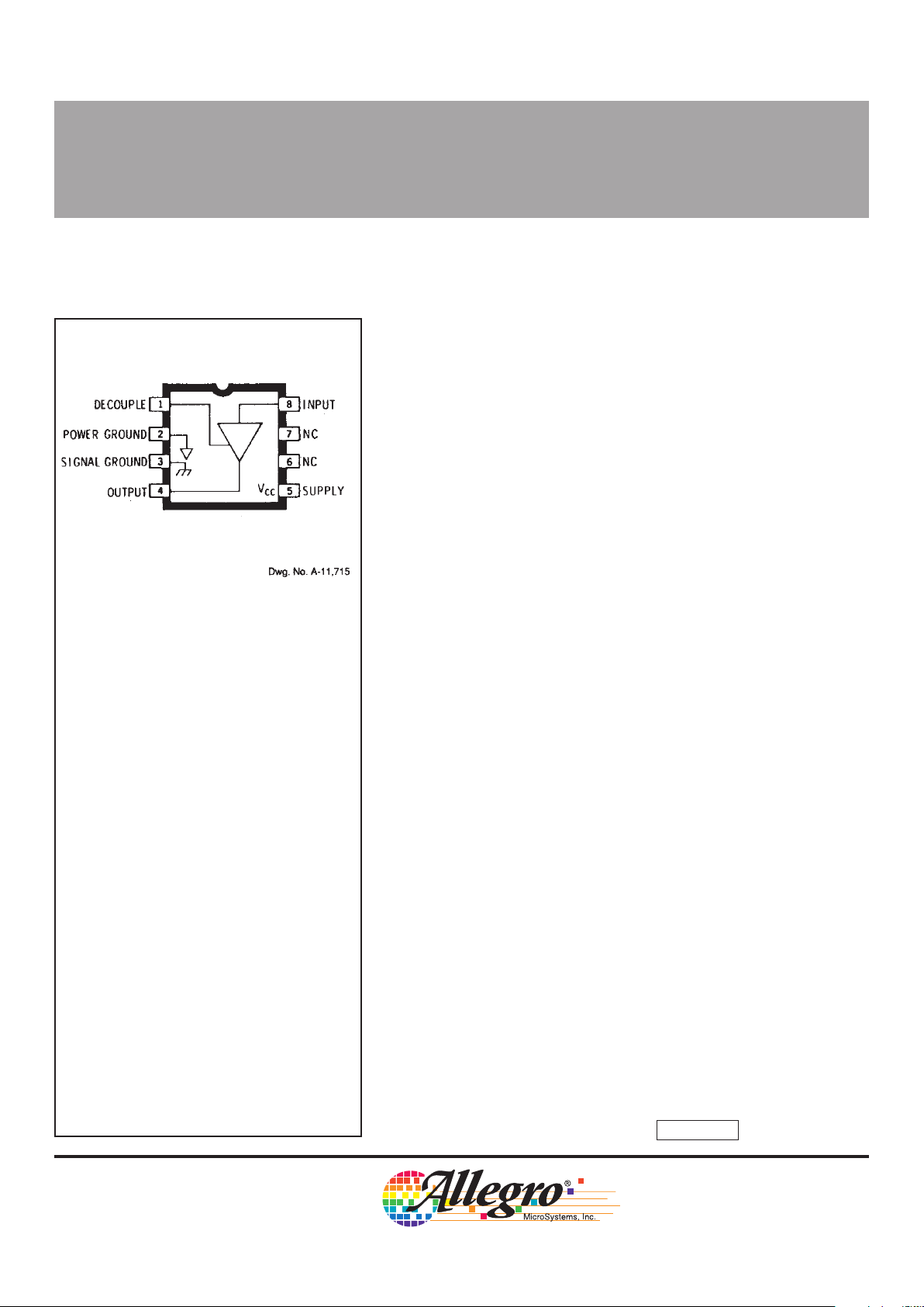
The ULN3718M audio amplifier is supplied in an 8-pin mini-DIP
plastic package. A copper alloy lead frame gives the amplifier enhanced power dissipation ratings.
FEATURES
■ Wide Operating Voltage Range 1.8 - 9.0 V
■ Low Quiescent Current
■ AC Short-Circuit Protection
■ Low External Parts Count
■ Low Distortion
■ 40 dB Voltage Gain
■ Low Noise
3718
LOW-VOLTAGE
AUDIO POWER AMPLIFIER
Always order by complete part number: ULN3718M .
Data Sheet
27117.25
ABSOLUTE MAXIMUM RATINGS
Supply Voltage, VCC. . . . . . . . . . . . . . 10 V
Package Power Dissipation,
P
D
. . . . . . . . . . . . . . . . . . . . See Graph
Operating Temperature Range,
T
A
. . . . . . . . . . . . . . . . -20°C to +85°C
Storage Temperature Range,
T
S
. . . . . . . . . . . . . . . -65°C to +150°C
Page 2
3718
LOW-VOLTAGE AUDIO POWER AMPLIFIER
115 Northeast Cutoff, Box 15036
Worcester, Massachusetts 01615-0036 (508) 853-5000
Limits
Characteristic Symbol Test Conditions Min. Typ. Max. Units
Supply Voltage Range V
CC
1.8 3.0 9.0 V
Quiescent Supply Current I
CC
VCC = 3.0 V — 6.0 10 mA
V
CC
= 6.0 V — 9.0 15 mA
VCC = 9.0 V — 12 20 mA
Voltage Gain A
V
36 40 44 dB
Audio Power Output P
OUT
RL = 8Ω, VCC = 3.0 V, THD = 10% — 80 — mW
RL = 8Ω, VCC = 6.0 V, THD = 10% 250 430 — mW
R
L
= 32Ω, VCC = 3.0 V, THD = 10% 15 25 — mW
R
L
= 32Ω, VCC = 6.0 V, THD = 10% — 125 — mW
Distortion THD P
OUT
= 10 mW — 0.3 1.0 %
P
OUT
= 1.0 mW, VCC = 1.8 V — 1.5 3.0 %
Output Noise V
out
Input Shorted, BW = 80 kHz — 200 500 µV
Input Resistance R
IN
Pin 8 — 250 — kΩ
Power Supply Rejection PSRR C
D
(Pin 1) = 500 µF, f = 120 Hz — 28 — dB
ELECTRICAL CHARACTERISTICS at T
A
= +25°C, V
CC
= 3 V, R
L
= 32Ω, f
in
= 400 Hz
(unless otherwise noted).
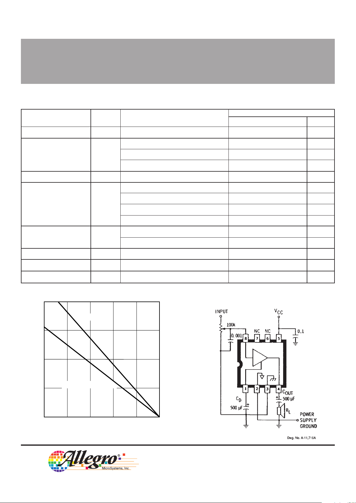
TEST CIRCUIT AND TYPICAL
APPLICATION
50 75 100 125 150
0.5
0
ALLOWABLE PACKAGE POWER DISSIPATION IN WATTS
TEMPERATURE IN °C
2.0
1.5
1.0
25
Dwg. GP-009-1B
R = 55°C/W
θJC
FREE AIR, R = 80°C/W
θJA
W
Copyright © 1985, 1995, Allegro MicroSystems, Inc.
Page 3

3718
LOW-VOLTAGE AUDIO POWER AMPLIFIER
TYPICAL CHARACTERISTICS
1000
R = 32 Ω
L
R = 16 Ω
L
R = 8 Ω
L
246810
200
0
800
600
400
0
Dwg. GS-010
SUPPLY VOLTAGE, V IN VOLTS
CC
THD = 10%
f = 400 Hz
in
OUTPUT POWER, P IN mW
OUT
POWER SUPPLY REJECTION RATIO
AS A FUNCTION OF FREQUENCY
OUTPUT POWER AS A
FUNCTION OF SUPPLY VOLTAGE
QUIESCENT SUPPLY CURRENT AS A
FUNCTION OF SUPPLY VOLTAGE
30 100 300 1k
30
40
0
10
20
10
Dwg. GS-012
FREQUENCY IN HERTZ
POWER SUPPLY REJECTION RATIO IN dB
C = 100 µF
D
C = 500 µF
D
246810
5
0
20
15
10
0
Dwg. GS-011
SUPPLY VOLTAGE, V IN VOLTS
CC
QUIESCENT SUPPLY CURRENT, I IN mA
CC
Page 4

3718
LOW-VOLTAGE AUDIO POWER AMPLIFIER
115 Northeast Cutoff, Box 15036
Worcester, Massachusetts 01615-0036 (508) 853-5000
APPLICATIONS INFORMATION
Selection of power-supply voltage and speaker impedance allows
a designer to choose audio power levels within the allowable package
power dissipation rating for any maximum operating temperature. No
unique precautions are necessary when designing with this device. It
is stable and ac short-circuit immune.
External component selection for this low-power amplifier involves
only two capacitors — one for output coupling and one for feedback
and ripple decoupling. The coupling capacitor value should be selected
to provide the desired low-frequency cutoff with the chosen load
impedance. The decoupling capacitor should be chosen for both
low-frequency audio rolloff and supply-ripple rejection.
Ripple rejection is not practical to calculate due to the large
number of mechanisms involved. A 500 µF capacitor achieves typically 25 dB rejection at 120 Hz.
The high gain and the high input impedance of the power amplifier
recommend use of this device in many diverse applications. However,
the input stage does have other characteristics that should be taken
into account for best results. The input is referenced to ground for
internal biasing and must be provided with a dc path to ground. A
current of typically 1 µA flows from the input through the volume
control. This produces an IR drop that is multiplied by the closed loop
dc gain of the amplifier and appears as an error in output centering.
This recommends a value of 200 kΩ or less for the volume control;
values of less than 100 kΩ are preferred.
The selection of amplifier load impedance involves more than just
consideration of the desired power output. A low load impedance will
produce the highest power output for any given supply voltage. Higher
impedances will furnish significant reduction in harmonic distortion and
improvement in overall repeatability in power output capacity.
Special steps toward minimizing tendencies towards instabilities
of all types were taken in the design of this device. However, as with
all high-gain circuits, care should be given to printed wiring board
layout to avoid undesirable effects. Inputs and outputs should be well
separated and should avoid common-mode impedances wherever
possible. For best performance, connect low-level input-signal ground
terminals and the decoupling capacitor ground terminal together at pin
3 (signal ground); connect the high-level speaker ground terminal and
the power supply ground terminal together at pin 2 (power ground).
The signal ground and the power ground should be interconnected
at only one point.
Page 5

3718
LOW-VOLTAGE AUDIO POWER AMPLIFIER
Dimensions in Inches
Dimensions in Millimeters
(Based on 1” = 25.4 mm)
0.355
0.204
7.62
BSC
Dwg. MA-001-8A mm
10.92
MAX
4
10.16
9.02
2.54
BSC
0.13
MIN
3.81
2.93
5
8
1
7.11
6.10
5.33
MAX
1.77
1.15
0.39
MIN
0.558
0.356
0.014
0.008
0.300
BSC
Dwg. MA-001-8A in
0.430
MAX
4
0.100
BSC
58
1
0.022
0.014
0.400
0.355
0.005
MIN
0.150
0.115
0.280
0.240
0.210
MAX
0.070
0.045
0.015
MIN
NOTES: 1. Lead thickness is measured at seating plane or below.
2. Lead spacing tolerance is non-cumulative.
3. Exact body and lead configuration at vendor’s option within limits shown.
Page 6

3718
LOW-VOLTAGE AUDIO POWER AMPLIFIER
115 Northeast Cutoff, Box 15036
Worcester, Massachusetts 01615-0036 (508) 853-5000
Allegro MicroSystems, Inc. reserves the right to make, from time to time, such departures from
the detail specifications as may be required to permit improvements in the design of its products.
Components made under military approvals will be in accordance with the approval requirements.
The information included herein is believed to be accurate and reliable. However, Allegro
MicroSystems, Inc. assumes no responsibility for its use; nor for any infringements of patents or
other rights of third parties which may result from its use.
 Loading...