

Page 1
CONTACT FACTORY
for availability
and latest information
ABSOLUTE MAXIMUM RATINGS
3625
AND
3626
POWERHALL® SENSOR/DRIVERS
FOR BRUSHLESS DC MOTORS
Requiring a minimum of external components, the UDN3625M
and UDN3626M are monolithic ICs that provide single-chip control
and direct drive solutions for many small, single-phase, unipolar
brushless dc motor applications. Integrated into the ICs are a highsensitivity Hall-effect sensor, control and commutating logic, a stable
voltage regulator, extensive self and system protective functions, and
two high-current saturated npn outputs. Both ICs include thermal
shutdown, output over-current limiting, and output transient protection/
flyback diodes. The UDN3625M is nominally for 12 V motor applications while the UDN3626M is better suited to 24 V motors.
Output over-current limiting (relating to startup surge or a locked
rotor condition) and short-circuit protection are provided by an internal
current-sense resistor. The maximum (default) output load current is
typically 1.3 A for the UDN3625M or 600 mA for the UDN3626M,
but may be decreased by user selection of an external low-wattage
resistor.
A separate low-level output provides tachometer capability for
motor speed control or sensing a locked rotor condition. With appropriate external logic, pulse-width modulated (PWM) speed control can
be accomplished at the output current adjust pin.
Data Sheet
27690A
Supply Voltage, VCC. . . . . . . . . . See Table
Output Current, I
PWM Current Control Voltage,
V
. . . . . . . . . . . . . See Applications
ADJ
Magnetic Flux Density, B . . . . . . Unlimited
Package Power Dissipation,
. . . . . . . . . . . . . . . . . . . . See Graph
P
D
Operating Temperature Range,
. . . . . . . . . . . . . . . . . -20°C to +85°C
T
A
Storage Temperature Range,
TS. . . . . . . . . . . . . . . . -65°C to +150°C
V
CC(MAX)
I
O(CONT)
I
O(PEAK)
Output current rating will be limited by
ambient temperature, supply voltage, and
duty cycle. Under any set of conditions, do
not exceed a junction temperature of
+150°C.
. . . . . . . . . . . . See Table
O
UDN3625M UDN3626M
14 V 26 V
1.0 A 0.45 A
1.6 A 0.75 A
These sensor/drivers are supplied in an 8-pin mini-DlP plastic
package with a copper leadframe for increased package power
handling capability.
FEATURES
■ 900 mA/12 V or 400 mA/24 V Operation
■ Speed-Control (PWM) Capability
■ Locked-Rotor Indication
■ Minimum External Components
■ Over-Current Protected
■ Thermal Protection
■ Enhanced Reliability
■ Reduced Cost
Always order by complete part number, e.g., UDN3625M .
See Maximum Ratings at left.
Page 2
3625
POWERHALL
AND
3626
®
SENSOR/DRIVERS FOR
BRUSHLESS DC MOTORS
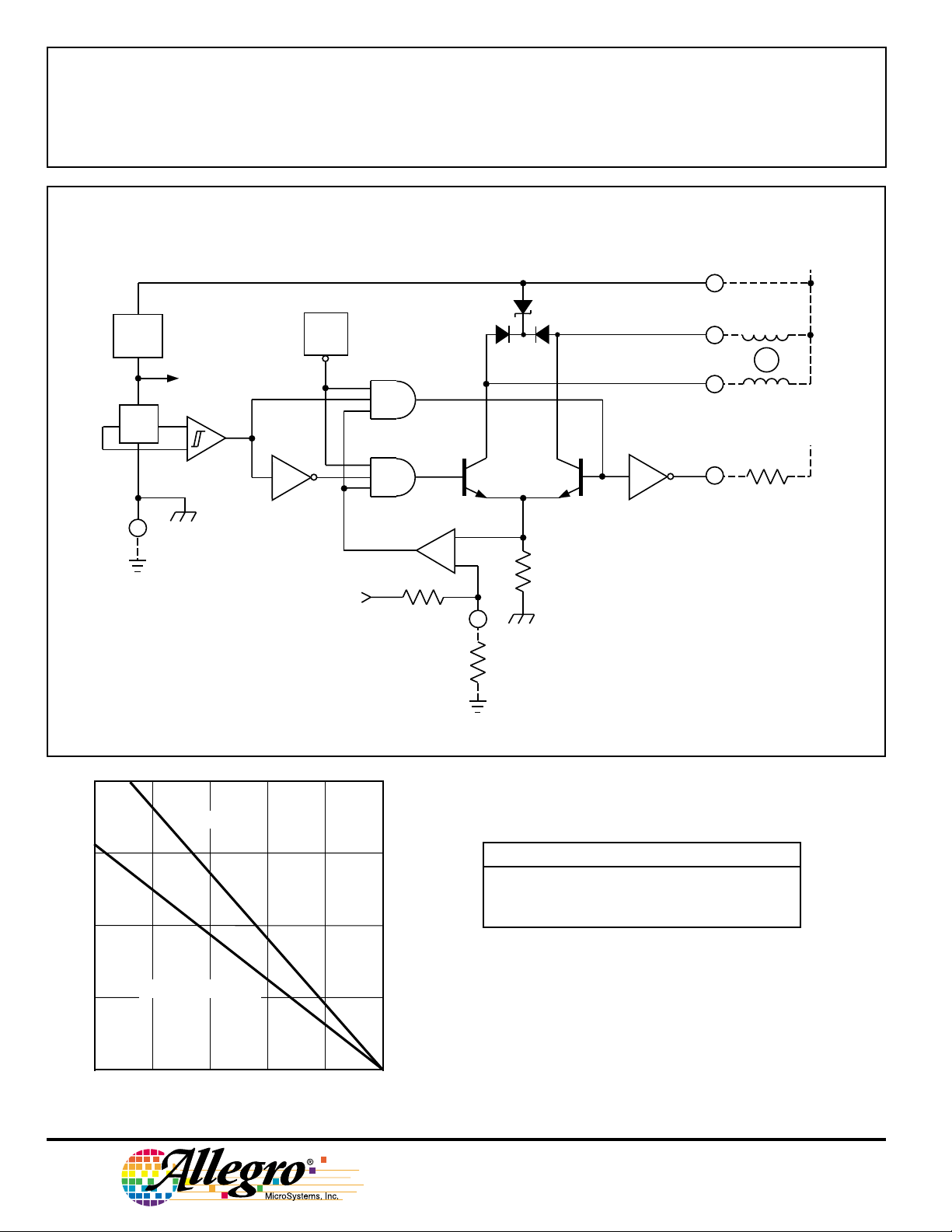
REG.
X
7
GROUND
TSD
FUNCTIONAL BLOCK DIAGRAM
SUPPLY
5
OUT
4
6
OUT
A
8
TACH
OUT
V
S
B
+V
2.0
R = 55°C/W
θJC
1.5
1.0
0.5
0
25
ALLOWABLE PACKAGE POWER DISSIPATION IN WATTS
FREE AIR, R = 80°C/W
50 75 100 125 150
θJA
TEMPERATURE IN °C
Dwg. GP-009-1B
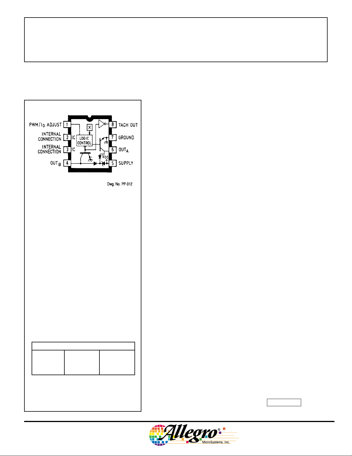
PWM/I
ADJUST
1
O
R
ADJ
TRUTH TABLE
Mag. Field PWM/IOADJ OUTAOUT
> +B
OP
> -B
OP
Any <0.3 V High High
Open Low High
Open High Low
Dwg. FP-005-1
B
115 Northeast Cutoff, Box 15036
Worcester, Massachusetts 01615-0036 (508) 853-5000
Copyright © 1988, 1995, Allegro MicroSystems, Inc.
Page 3

3625
AND
3626
POWERHALL
®
SENSOR/DRIVERS FOR
BRUSHLESS DC MOTORS
ELECTRICAL CHARACTERISTICS at T
= +25°C, R
A
= ∞, Over Operating Voltage Range
ADJ
(unless otherwise noted).
Limits
Characteristic Symbol Test Conditions Min. Typ. Max. Units
UDN3625M
Operating Voltage Range V
Output Leakage Current I
Output Breakdown Voltage V
Output Saturation Voltage V
S
O
(BR)CEX
O(SAT)
Output Current Limit IO MAX R
Output Clamp Voltage
V
CL
(Test Fig. 1)
Output Switching Time t
Supply Current
PLH
l
CC
(Test Fig. 2)
UDN3626M
VCC = VO = 24 V — — 100 µA
VCC = 24 V, lO = 10 mA* 34 — — V
IO = 450 mA, VS = 6.5 V — 0.25 0.4 V
IO = 900 mA, VS = 12 V — 0.5 0.8 V
= ∞, VO = 2 V 1.0 1.3 1.6 A
ADJ
ICL = 10 mA, VCC = 0 11 12 13 V
ICL = 450 mA=, VCC = 0 13 14 15 V
50% V
R
ADJ
R
ADJ
to VO = 3.0 V, lO = 450 mA — — 5.0 µs
ADJ
= ∞, VS = 14 V, One Output ON — 30 38 mA
= 0 Ω, VS = 14 V, Outputs OFF — 8.0 10 mA
6.5 12 14 V
Operating Voltage Range V
Output Leakage Current l
Output Breakdown Voltage V
Output Saturation Voltage V
S
O
(BR)CEX
O(SAT)
VCC = VO = 30 V — — 100 µA
VCC = 30 V, lO = 10 mA* 50 — — V
lO = 250 mA, VS = 6.5 V — 0.15 0.3 V
lO = 400 mA, VS = 24 V — 0.3 0.5 V
Output Current Limit lOMAX R
Output Clamp Voltage
V
CL
(Test Fig. 1)
Output Switching Time t
Supply Current l
PLH
CC
(Test Fig. 2)
= ∞, VO = 2 V 450 600 750 mA
ADJ
ICL = 10 mA, VCC = 0 17 18 20 V
ICL = 250 mA, VCC = 0 19 20 22 V
50% V
R
ADJ
R
ADJ
to VO = 3.0 V, lO = 250 mA — — 5.0 µs
ADJ
= ∞, VS = 26 V, One Output ON — — 24 mA
= 0 Ω, VS = 26 V, Outputs OFF — 8.0 10 mA
*lO is almost entirely Zener clamp current.
† Pulse test.
‡ Dependent on value of external series Zener diode (see Applications), 6.5 V without a Zener diode.
‡2426 V
Continued next page...
Page 4

3625
POWERHALL
AND
3626
®
SENSOR/DRIVERS FOR
BRUSHLESS DC MOTORS
ELECTRICAL CHARACTERISTICS continued
Limits
Characteristic Symbol Test Conditions Min. Typ. Max. Units
Both
Operate Point§ B
Hysteresis B
Output Current Limit Ratio lO/lO MAX R
PWM Control Current I
Tach Output Leak. Current I
Tach Output Sat. Voltage V
Thermal Shutdown T
Thermal Hysteresis ∆T
OP
H
ADJ
T
T(SAT)
J
J
= 39 kΩ — 0.75 — —
ADJ
R
= 17 kΩ — 0.50 — —
ADJ
R
= 10 kΩ — 0.25 — —
ADJ
V
= 0 — -350 -500 µA
ADJ
V
= 14 V — — 10 µA
T
IT = 750 µA — 0.2 0.4 V
— ±100 ±150 G
— 200 — G
–– 165 — °C
–– 10 — °C
§ Magnetic flux density is measured at most sensitive area of device, nominally located 0.055" (1.40 mm) below the top of the package.
OUTPUT CLAMP VOLTAGE TEST
SUPPLY CURRENT TEST
(ONE OUTPUT TESTED AT A TIME)
Dwg. No. EP-013
TEST FIG. 2 TEST FIG. 1
115 Northeast Cutoff, Box 15036
Worcester, Massachusetts 01615-0036 (508) 853-5000
Page 5

3625
AND
POWERHALL
SENSOR/DRIVERS FOR
BRUSHLESS DC MOTORS
SENSOR LOCATION APPLICATIONS INFORMATION
Power Dissipation. Care should be taken in evaluating the package power
dissipation of these devices. Total power dissipated by the device will consist
of power due to the internal regulator, logic and drive circuitry (ICC x VCC),
power due to the output drivers (IO x V
circuitry (ICL x VCL x duty cycle).
For example:
ICC x VCC = 38 mA (max) x 14 V = 532 mW (max)
), and power due to the clamp
O(SAT)
3626
®
IO x V
ICL x VCL x duty cycle = 450 mA x 15 V (max) x 1% = 67.5 mW (max)
Some of the power dissipated by the device (ICC x VCC) can be reduced
by inserting a Zener diode in the supply line (ZA in the figure). Note that the
voltage at the VCC pin under worst-case conditions must be greater than the
minimum operating voltage (6.5 V).
Transient Protection. A note of caution concerns negative (below ground)
excursions of the outputs. In application, the coupling of the two motor
windings can provide for just such a case. Reducing the coupling between
windings will help, but ground clamp diodes or diodes in series with the
motor windings might be required (DC or DS in the figure). Most small
brushless motors will not require these diodes.
System requirements usually utilize a diode type of reverse-polarity
protection. If series diode protection is used with an inductive load (the usual
fan application), a Zener clamp between VS and ground (ZB in the figure) is
required. The Zener voltage must be greater than the supply voltage but less
than the rated maximum allowable supply voltage.
With diode reverse-polarity protection, a high-impedance supply, or a
switched supply line, high-voltage spikes will be generated (especially with
high-current or high-inductance loads) during normal operation, coasting, or
immediately after turn-off. In these situations, a Zener clamp (ZB) from VS to
ground will be required.
= 450 mA x 0.4 V (max) = 180 mW (max)
O(SAT)
Total package power dissipation = 779.5 mW (max)
Over-Current Adjust Pin. The over-current limit may be reduced from the
default value (IO MAX) by selection of an external resistor (R
PWM/IO ADJ pin.
ADJ
) at the
Page 6

3625
POWERHALL
AND
3626
®
SENSOR/DRIVERS FOR
BRUSHLESS DC MOTORS
TYPICAL FAN APPLICATION
The external overcurrent adjust and the thermal shutdown are commoned
at the PWM/lO ADJ pin and tieing it to VCC will disable the thermal shutdown. PWM current/speed control can be performed at the PWM/lO ADJ pin
from a standard totem-pole logic output with a series Schottky diode
(1N5818,1N5819, or equivalent) or by pulling it low through an opencollector transistor (no pull-up resistor). PWM/lO ADJ input voltages greater
than 0.3 V are not recommended and may create an unstable operating
condition.
OUT ON/LOW
MAGNETIC FIELD
A
DEFINITIONS
+B
S
+B
N
Dwg. AP-001-1
-B
OUT ON/LOW
B
-B
O P
B = 0 G
By accepted magnetic convention, lines of flux emanate from the north pole of a magnet and enter the south pole.
115 Northeast Cutoff, Box 15036
Worcester, Massachusetts 01615-0036 (508) 853-5000
O P
Dwg. GP-008
+B
Page 7

0.280
0.240
Dimensions in Inches
(controlling dimensions)
58
3625
AND
3626
POWERHALL
®
SENSOR/DRIVERS FOR
BRUSHLESS DC MOTORS
0.014
0.008
0.430
MAX
0.300
BSC
0.100
BSC
4
1
0.070
0.045
0.210
MAX
0.015
MIN
0.022
0.014
NOTES: 1. Leads 1, 4, 5, and 8 may be half leads at vendor’s option.
2. Lead thickness is measured at seating plane or below.
3. Lead spacing tolerance is non-cumulative.
4. Exact body and lead configuration at vendor’s option
within limits shown.
0.400
0.355
0.005
MIN
0.150
0.115
Dwg. MA-001-8A in
Page 8

3625
POWERHALL
AND
3626
®
SENSOR/DRIVERS FOR
BRUSHLESS DC MOTORS
8
7.11
6.10
Dimensions in Millimeters
(for reference only)
5
0.355
0.204
7.62
BSC
10.92
MAX
1
4
1.77
1.15
10.16
9.02
5.33
MAX
0.39
MIN
0.558
0.356
NOTES: 1. Leads 1, 4, 5, and 8 may be half leads at vendor’s option.
2. Lead thickness is measured at seating plane or below.
3. Lead spacing tolerance is non-cumulative.
4. Exact body and lead configuration at vendor’s option
within limits shown.
2.54
BSC
0.13
MIN
3.81
2.93
Dwg. MA-001-8A mm
The products described herein are manufactured under one or
more of the following U.S. patents: 5,045,920; 5,264,783; 5,442,283;
5,389,889; 5,581,179; 5,517,112; 5,619,137; 5,621,319; 5,650,719;
5,686,894; 5,694,038; 5,729,130; 5,917,320; and other patents
pending.
Allegro MicroSystems, Inc. reserves the right to make, from time to
time, such departures from the detail specifications as may be
required to permit improvements in the performance, reliability, or
manufacturability of its products. Before placing an order, the user is
cautioned to verify that the information being relied upon is current.
Allegro products are not authorized for use as critical components
in life-support appliances, devices, or systems without express written
approval.
The information included herein is believed to be accurate and
reliable. However, Allegro MicroSystems, Inc. assumes no responsibility for its use; nor for any infringements of patents or other rights of
third parties that may result from its use.
115 Northeast Cutoff, Box 15036
Worcester, Massachusetts 01615-0036 (508) 853-5000
 Loading...