

Page 1
2993
DUAL H-BRIDGE
MOTOR DRIVERS
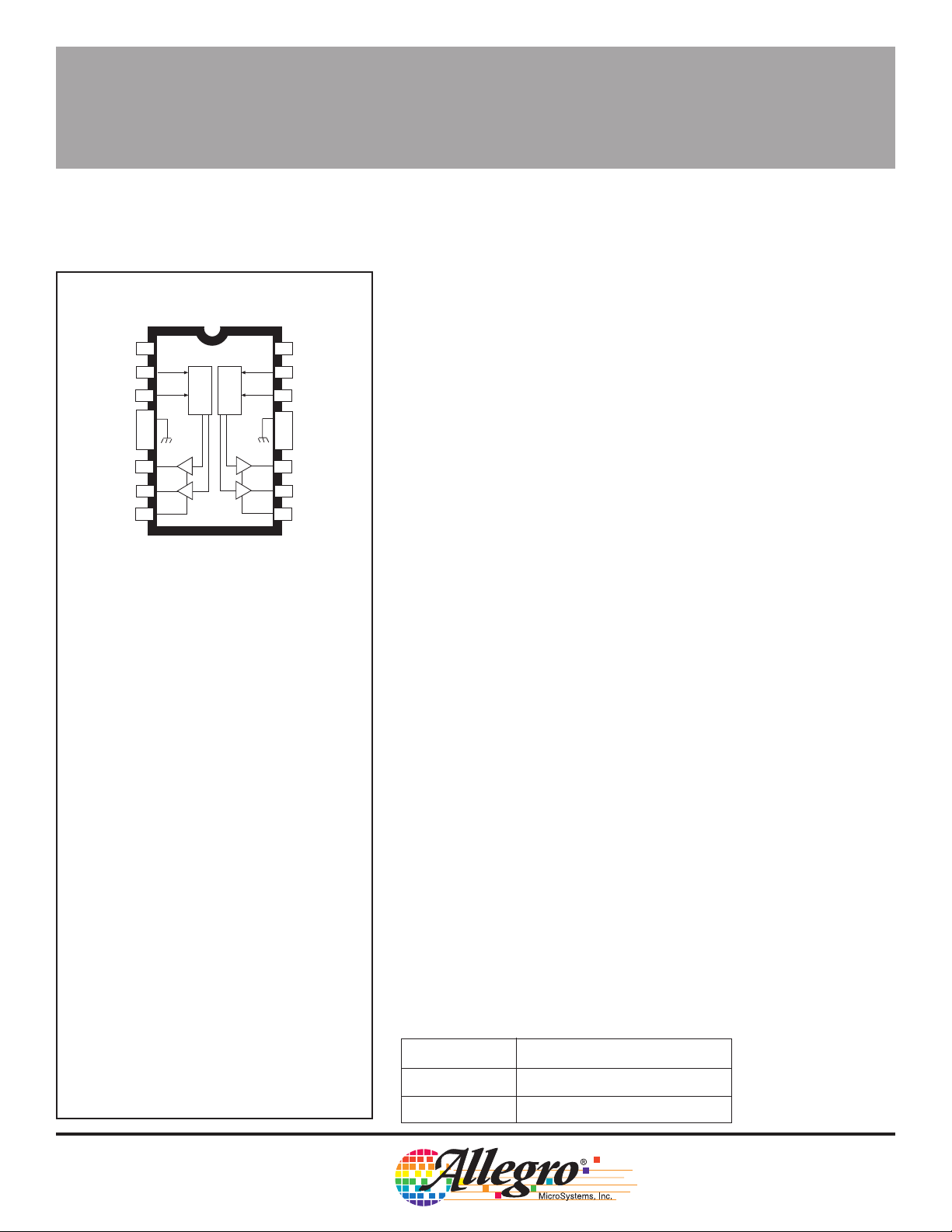
UDN2993B
LOAD SUPPLY
ENABLE
PHASE
GROUND
GROUND
OUT
OUT
V
V
BB
1
2
A
3
A
4
5
6
1A
7
2A
8
EA
LOGIC
V
LOGIC
DD
16
15
14
13
12
11
10
9
Dwg. No. A-12,455
LOGIC SUPPLY
ENABLE
B
PHASE
B
GROUND
GROUND
OUT
1B
OUT
2B
V
EB
2993
DUAL H-BRIDGE MOTOR DRIVERS
Cost-effective monolithic drive electronics for bipolar stepper and
dc (brush) servo motors to 30 V and 500 mA is very practical with the
UDN2993B and UDN2993LB. These dual full-bridge motion control
ICs integrate separate inputs, level shifting for upper power outputs,
control logic, integral inductive transient protection, and source (upper)
and sink (lower) drivers in an H-bridge configuration. The single-chip
power IC provides improved space utilization and reliability unmatched
by discrete component circuitry.
Excepting the power supply connections, the two H-bridges are
independent. An ENABLE input is provided for each bridge and
permits pulse-width modulation (PWM) through the use of external
circuitry. PWM drive techniques provide the benefits of reduced power
dissipation, improved motor performance (especially torque), and
positively affect system efficiency. Separate PHASE inputs for each
bridge determine the direction of current flow in the load. Additionally,
each pair of (sink) emitters are terminated to package connections.
This allows the use of current-sensing circuitry. Both devices
incorporate an intrinsic “dead time” to preclude high crossover
(or cross-conduction) currents during changes in direction (phase).
Data Sheet
29319.5A
These devices are packaged in plastic DIPs (suffix B) or surface-
ABSOLUTE MAXIMUM RATINGS
at T
≤ +150°C
J
mountable wide-body SOICs (suffix LB) with copper lead frames for
optimum power dissipation without heat sinks. The lead configurations
allow automatic insertion, fit standard IC sockets or printed wiring
Load Supply Voltage, VBB.................... 30 V
Logic Supply Voltage, VDD................... 7.0 V
Logic Input Voltage Range, V
V
Output Current, I
............... -0.3 V to VDD + 0.3 V
ENABLE
..................... ±600 mA
OUT
PHASE
or
Sink Driver Emitter Voltage,
.................................................. 1.5 V
V
E
Package Power Dissipation,
........................................ See Graph
P
D
Operating Temperature Range,
................................. -20°C to +85°C
T
A
DISCONTINUED PRODUCT
Storage Temperature Range,
............................... -55°C to +150°C
T
S
IMPORTANT: Load supply voltage must never be
applied without logic supply voltage present.
NOTE: Output current rating may be limited by
chopping frequency, ambient temperature,
airflow, and heat sinking. Under any set of
conditions, do not exceed the specified maximum
current and a junction temperature of +150°C.
— FOR REFERENCE ONLY
board layouts, and enable easy attachment of a heat sink for maximum
power-handling capability. The heat-sink tabs are at ground potential
and require no insulation.
Dual full-bridge drivers with peak current ratings of ±3 A are
supplied as the UDN2998W.
FEATURES
■ ±600 mA Output Current
■ Output Voltage to 30 V
■ Crossover Current Protection
■ TTL/NMOS/CMOS Compatible Inputs
■ Low Input Current
■ Internal Clamp Diodes
■ Automotive Capable
Always order by complete part number:
Part Number Package
UDN2993B 16-Pin DIP
UDN2993LB 20-Lead Wide-Body SOIC
Page 2
2993
DUAL H-BRIDGE
MOTOR DRIVERS
UDN2993LB
LOAD
SUPPLY
ENABLE
PHASE
GROUND
GROUND
GROUND
GROUND
OUT
OUT
V
V
1
BB
2
A
3
A
4
5
6
7
8
1A
9
2A
10
EA
LOGIC
LOGIC
V
DD
20
19
18
17
16
15
14
13
12
11
LOGIC
SUPPLY
ENABLE
PHASE
GROUND
GROUND
GROUND
GROUND
OUT
1B
OUT
2B
V
EB
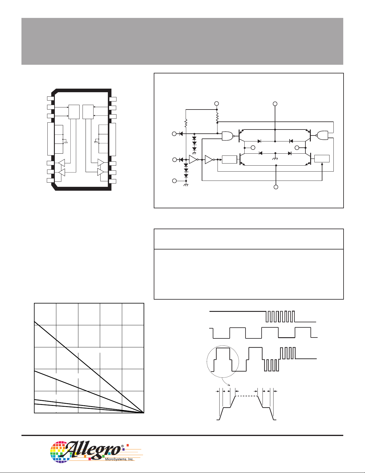
FUNCTIONAL BLOCK DIAGRAM
(One of Two Drivers)
V
B
B
ENABLE
PHASE
GROUND
DD
TURN-ON
DELAY
OUT
V
BB
OUT
1
2
TURN-ON
DELAY
V
E
Dwg. No. A-14,340
Dwg. No. A-12,447
TRUTH TABLE
Enable Phase
Input Input Output 1 Output 2
High High Low High
High Low High Low
Low High Low Open
Low Low Open Low
25
V
ENABLE
20
V
PHASE
15
10
SUFFIX 'B', R = 13°C/W
SUFFIX 'LB', R = 6.0°C/W
θJT
θJT
I
+
OUT
_
5
SUFFIX 'B', R = 40°C/W
ALLOWABLE PACKAGE POWER DISSIPATION IN WATTS
SUFFIX 'LB', R = 61°C/W
0
25
θJA
θJA
50 75 100 125 150
TEMPERATURE IN °C
Dwg. GP-021A
t
t
t
f
r
d
t
t
f
d
115 Northeast Cutoff, Box 15036
W
Worcester, Massachusetts 01615-0036 (508) 853-5000
Copyright © 1985, 1993, Allegro MicroSystems, Inc.
t
r
Dwg. No. A-12,448
Page 3
2993
DUAL H-BRIDGE
MOTOR DRIVERS
ELECTRICAL CHARACTERISTICS at T
= +25°C, V
A
= 30 V, VDD = 5 V, VE = 0 V, T
BB
≤ +150°C
J
Figure 1 (unless otherwise noted).
Limits
Characteristic Symbol Test Conditions Min. Typ. Max. Units
Output Drivers
Operating Voltage Range V
Output Leakage Current I
Output Saturation Voltage V
Output Sustaining Voltage V
Motor Supply Current I
CE(sus)
BB(ON)
I
BB(OFF)
Source Driver Rise Time t
Source Driver Fall Time t
Clamp Diode Forward Voltage V
Control Logic (PHASE or ENABLE)
Logic Input Current I
I
Logic Input Voltage V
V
Logic Supply Current I
Turn-On Delay Time t
Turn-Off Delay Time t
BB
CEX
CE(SAT)
r
f
F
IN(1)
IN(0)
IN(1)
IN(0)
DD
pd0
pd1
V
V
V
V
I
V
V
I
I
= 0.8 V, V
ENABLE
= 0.8 V, V
ENABLE
= 2.4 V, I
ENABLE
= 2.4 V, I
ENABLE
= ±500 mA, Figure 2, Note 2 30 — — V
OUT
= 2.4 V, Outputs Open, Note 2 — 1.0 3.0 mA
ENABLE
= 0.8 V, Outputs Open, Note 2 — 250 300 µA
ENABLE
= -500 mA — 75 — ns
OUT
= -500 mA — 280 — ns
OUT
= VBB, Note 2 — < 1.0 50 µA
OUT
= 0 V, Note 2 — < -1.0 -50 µA
OUT
= 500 mA — 1.6 1.8 V
OUT
= -500 mA — 1.6 2.0 V
OUT
IF = 500 mA — 1.6 1.8 V
V
PHASE
V
PHASE
or V
or V
= 2.4 V — < 1.0 10 µA
ENABLE
= 0.8 V — -200 -300 µA
ENABLE
ENABLE Input to Source Drivers — 250 — ns
ENABLE lnput to Source Drivers — 500 — ns
10 — 30 V
2.4 — — V
— — 0.8 V
—1420mA
NOTES: 1. Each driver is tested separately.
2. Test is performed with V
3. Negative current is defined as coming out of (sourcing) the specified device pin.
PHASE
= 0.8 V and then repeated for V
PHASE
= 2.4 V.
Page 4

2993
INPUT
INPUT
A
B
0
0
+5V
+5V
DUAL H-BRIDGE
MOTOR DRIVERS
TEST FIGURES
FIGURE 1
= 5V
V
DD
ENABLE
OUT
1
PHASE
GROUND
2.4V
0.8V
TURN-ON
DELAY
FIGURE 2
= 5V
V
DD
= 40V
V
BB
I
OUT
mA
V
E
OUT
2
TURN-ON
DELAY
Dwg. No. A-12,449
TYPICAL APPLICATION
2-PHASE BIPOLAR STEPPER MOTOR DRIVE
= 40V
V
BB
(Chopper Mode)
ENABLE
PHASE
GROUND
TURN-ON
DELAY
+5V
10K
0.1
10K
Dwg. No. A-12,453
5.6K
_
+
470K
10K
0.1
10K
IN
+36V
A
+ 5V
1Ω
LOGIC
LOGIC
V
DD
16
15
IN
B
14
13
12
11
10
9
V
BB
1
2
3
4
5
6
7
8
1Ω
0.1
1K
56Ω
mH
2
TURN-ON
DELAY
V
E
Dwg. No. A-12,450
+5V
5.6K
_
+
470 K
Dwg. No. A-12,454
115 Northeast Cutoff, Box 15036
Worcester, Massachusetts 01615-0036 (508) 853-5000
Page 5

2993
DUAL H-BRIDGE
MOTOR DRIVERS
16
0.280
0.240
UDN2993B
Dimensions in Inches
NOTE 4
0.020
9
0.008
0.300
BSC
0.430
MAX
0.210
MAX
7.11
6.10
0.015
MIN
1
0.070
0.045
16
1
1.77
1.15
0.022
0.014
8
0.150
0.115
0.775
0.735
0.100
BSC
Dimensions in Millimeters
(Based on 1” = 25.4 mm)
NOTE 4
19.68
18.67
2.54
BSC
9
8
0.005
MIN
0.13
MIN
0.508
0.204
Dwg. MA-001-17A in
10.92
MAX
7.62
BSC
5.33
MAX
0.39
MIN
0.558
0.356
NOTES: 1. Exact body and lead configuration at vendor’s option within limits shown.
2. Lead spacing tolerance is non-cumulative
3. Lead thickness is measured at seating plane or below.
4. Webbed lead frame. Leads 4, 5, 12, and 13 are internally one piece.
3.81
2.93
Dwg. MA-001-17A mm
Page 6

2993
D
DUAL H-BRIDGE
MOTOR DRIVERS
UDN2993LB
Dimensions in Inches
(Based on 1 mm = 0.03937”)
0.2992
0.2914
0.020
0.013
0.0926
0.1043
20 11
1 2
0.0040
MIN.
3
0.5118
0.4961
Dimensions in Millimeters
20
11
0.050
BSC
NOTE 1
NOTE 3
0.419
0.394
0° TO 8°
0.0125
0.0091
0.050
0.016
wg. MA-008-21A in
0.32
0.23
7.60
7.40
0.51
0.33
2.65
2.35
1
0.10
2
MIN.
3
13.00
12.60
1.27
BSC
NOTE 1
NOTE 3
10.65
10.00
0° TO 8°
Dwg. MA-008-21A mm
1.27
0.40
NOTES: 1. Webbed lead frame. Leads 5, 6, 15, and 16 are internally one piece.
2. Lead spacing tolerance is non-cumulative.
3. Exact body and lead configuration at vendor’s option within limits shown.
115 Northeast Cutoff, Box 15036
Worcester, Massachusetts 01615-0036 (508) 853-5000
Page 7

2993
DUAL H-BRIDGE
MOTOR DRIVERS
This page intentionally left blank
Page 8

2993
DUAL H-BRIDGE
MOTOR DRIVERS
MOTOR DRIVERS SELECTION GUIDE
Function Output Ratings * Part Number †
INTEGRATED CIRCUITS FOR BRUSHLESS DC MOTORS
3-Phase Controller/Drivers ±2.0 A 45 V 2936 and 2936-120
Hall-Effect Latched Sensors 10 mA 24 V 3175 and 3177
2-Phase Hall-Effect Sensor/Controller 20 mA 25 V 3235
Hall-Effect Complementary Output Sensor 20 mA 25 V 3275
2-Phase Hall-Effect Sensor/Driver 900 mA 14 V 3625
2-Phase Hall-Effect Sensor/Driver 400 mA 26 V 3626
Hall-Effect Comp. Output Sensor/Driver 300 mA 60 V 5275
3-Phase Back-EMF Controller/Driver ±900 mA 14 V 8902–A
3-Phase Controller/DMOS Driver ±4.0 A 14 V 8925
3-Phase Back-EMF Controller/Driver ±1.0 A 7 V 8984
INTEGRATED BRIDGE DRIVERS FOR DC AND BIPOLAR STEPPER MOTORS
PWM Current Controlled Dual Full Bridge ±750 mA 45 V 2916
PWM Current Controlled Dual Full Bridge ±1.5 A 45 V 2917
PWM Current Controlled Dual Full Bridge ±1.5 A 45 V 2918
PWM Current Controlled Dual Full Bridge ±750 mA 45 V 2919
Dual Full Bridge Driver ±2.0 A 50 V 2998
PWM Current Controlled Full Bridge ±2.0 A 50 V 3952
PWM Current Controlled Full Bridge ±1.3 A 50 V 3953
PWM Current Controlled Dual Full Bridge ±800 mA 45 V 3961
PWM Current Controlled Dual Full Bridge ±800 mA 30 V 3962
OTHER INTEGRATED CIRCUIT & PMCM MOTOR DRIVERS
Unipolar Stepper Motor Quad Driver 1.8 A 50 V 2544
Unipolar Stepper-Motor Translator/Driver 1.25 A 50 V 5804
Unipolar Stepper-Motor Quad Driver 1 A 46 V 7024 and 7029
Unipolar Microstepper-Motor Quad Driver 1.2 A 46 V 7042
Voice-Coil Motor Driver ±500 mA 6 V 8932-A
Voice-Coil Motor Driver ±800 mA 16 V 8958
Voice-Coil (and spindle) Motor Driver ±350 mA 7 V 8984
* Current is maximum specified test condition, voltage is maximum rating. See specification for sustaining
voltage limits or over-current protection voltage limits.
Negative current is defined as coming out of (sourcing) the output.
† Complete part number includes additional characters to indicate operating temperature range and package style.
Allegro MicroSystems, Inc. reserves the right to make, from time to time, such departures from the
detail specifications as may be required to permit improvements in the design of its products.
Components made under military approvals will be in accordance with the approval requirements.
The information included herein is believed to be accurate and reliable. However, Allegro
MicroSystems, Inc. assumes no responsibility for its use; nor for any infringements of patents or other
rights of third parties which may result from its use.
115 Northeast Cutoff, Box 15036
Worcester, Massachusetts 01615-0036 (508) 853-5000
 Loading...