

Page 1
Data Sheet
29310.2A†
2985
8-CHANNEL SOURCE DRIVER
Recommended for applications requiring separate logic and load grounds,
load supply voltages to 30 V, and load currents to 250 mA, the UDN2985A
source driver is used as an interface between standard low-power digital logic
1
2
3
4
5
6
7
8
V
S
18
17
16
15
14
13
12
11
GND
Dwg. No. A-10,243
and LEDs, relays, and solenoids. The outputs feature saturated transistors for
low collector-emitter saturation voltages.
The UDN2985A driver is for use with 5 V logic systems: TTL, Schottky
TTL, DTL, and CMOS. This device has a minimum output breakdown rating
of 30 V with a minimum output sustaining voltage of 15 V. The output is
switched on by an active-high input level.
Under normal operating conditions, this device can source up to 120 mA
for each of the eight outputs at an ambient temperature of 75°C and a supply
voltage of 15 V. It incorporates input current-limiting resistors and output
transient-suppression diodes.
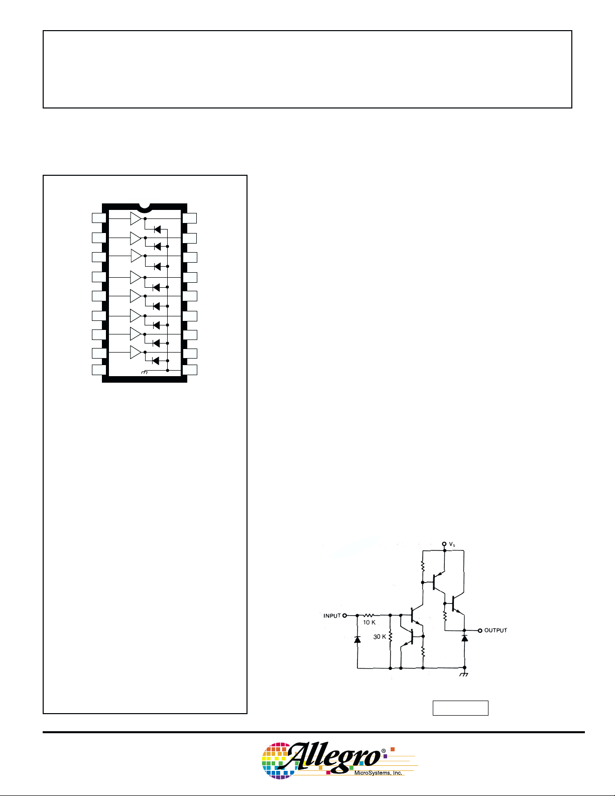
The UDN2985A source driver is supplied in an 18-pin dual in-line
package. All inputs are on one side of the package, output pins on the other,
to simplify printed wiring board layout.
ABSOLUTE MAXIMUM RATINGS
at T
= 25°C
A
Driver Supply Voltage, VS.................. 30 V
Continuous Output Current,
I
........................................ -250 mA
OUT
Input Voltage, VIN............................... 20 V
Package Power Dissipation,
PD.............................................. 2.2 W*
Operating Temperature Range,
TA............................... -20°C to +85°C
Storage Temperature Range,
TS............................... -55°C to +150°C
*Derate at the rate of 18 mW/°C above
TA= 25°C.
FEATURES
■ TTL, DTL, or CMOS Compatible Inputs
■ 250 mA Output Source Current Capability
■ Output Transient-Suppression Diodes
■ 30 V Minimum Output Breakdown Voltage
■ Low Output-Saturation Voltage
PARTIAL SCHEMATIC DIAGRAM
1 of 8 DRIVERS
Dwg. No. DS-1013
Always order by complete part number: UDN2985A .
Page 2
2985
8-CHANNEL
SOURCE DRIVER
ELECTRICAL CHARACTERISTICS at TA = 25°C, VS = 30 V (unless otherwise noted).
Limits
Characteristics Symbol Test Conditions Min. Typ. Max. Units
Output Leakage Current I
Output Sustaining Voltage V
Output Saturation Voltage V
Input Current Voltage I
Supply Current I
CEX
CE(sus)
CE(SAT)
IN(ON)
I
IN(OFF)
S
VIN = 0.4 V, V
l
= -120 mA, L = 3 mH 15 — — V
OUT
V
= 2.4, l
IN
= 2.4, l
V
IN
VIN = 2.4 V — 90 225 µA
= 5.0 V — 280 650 µA
V
IN
VIN = 0.4 V — 10 15 µA
VS = 30 V, VIN = 2.4 V — 10 15 mA
= 0 V — <-1.0 -100 µA
OUT
= -60 mA — 0.8 1.1 V
OUT
= -120 mA — 0.9 1.2 V
OUT
(outputs open)
Clamp Diode I
R
VR = 30 V, TA = 70°C — <1.0 50 µA
Leakage Current
Clamp Diode V
F
IF = 120 mA — 1.1 2.0 V
Foward Voltage
Turn-On Delay t
Turn-Off Delay t
ON
OFF
NOTE: Negative current is defined as coming out of (sourcing) the specified device pin.
— 0.5 1.0 µs
— 5.0 10 µs
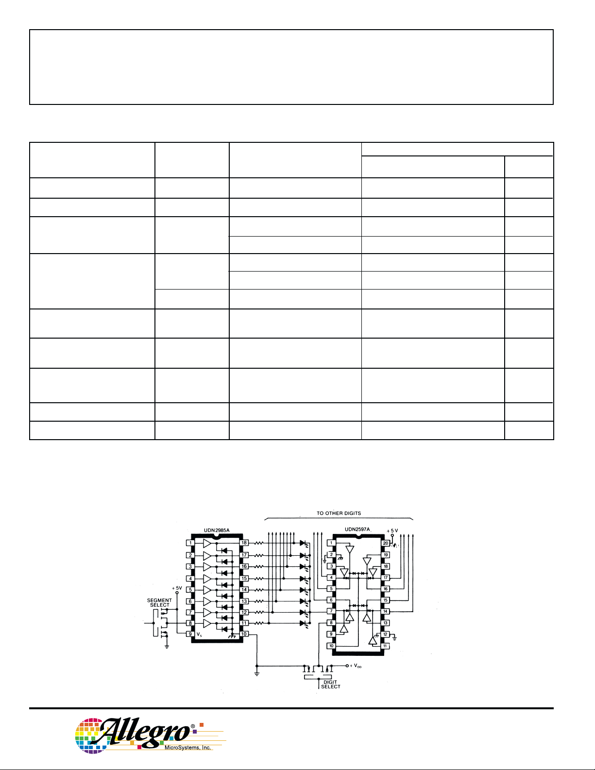
COMMON-CATHODE LED DRIVER
115 Northeast Cutoff, Box 15036
Worcester, Massachusetts 01615-0036 (508) 853-5000
Copyright © 1984, 2000 Allegro MicroSystems, Inc.
Dwg. No. DS-1014
Page 3

0.280
0.240
18
Dimensions in Inches
(controlling dimensions)
10
2985
8-CHANNEL
SOURCE DRIVER
0.014
0.008
0.430
MAX
0.300
BSC
0.210
MAX
7.11
6.10
0.015
MIN
18
1
0.070
0.045
0.022
0.014
0.920
0.880
0.100
BSC
9
0.005
MIN
0.150
0.115
Dwg. MA-001-18A in
Dimensions in Millimeters
(for reference only)
0.355
10
1
1.77
1.15
23.37
22.35
2.54
BSC
9
0.13
MIN
0.204
7.62
BSC
10.92
MAX
5.33
MAX
0.39
MIN
0.558
0.356
NOTES: 1. Exact body and lead configuration at vendor’s option within limits shown.
2. Lead spacing tolerance is non-cumulative.
3. Lead thickness is measured at seating plane or below.
4. Supplied in standard sticks/tubes of 21 devices.
3.81
2.93
Dwg. MA-001-18A mm
Page 4

2985
8-CHANNEL
SOURCE DRIVER
POWER SOURCE DRIVERS
IN ORDER OF 1) OUTPUT CURRENT, 2) OUTPUT VOLTAGE, 3) NUMBER OF DRIVERS
Output Ratings *
Serial Latched Diode Saturated Internal
mA V # Input Drivers Clamp Outputs Protection Part Number
-25 60 8 – X – – – 5815
60 10 X X active pull-down – – 5810-F and 6809/10
60 12 X X active pull-down – – 5811 and 6811
60 20 X X active pull-down – – 5812-F and 6812
60 32 X X active pull-down – – 5818-F and 6818
85 8 –––– –6118
-120 -25 8 – – X X – 2585
30 8 – – X X – 2985
50 8 X X X X – 5895
-350 35 8 – – X – X 2987
50 8 – – X – – 2981 and 2982
50 8 X X X – – 5891
-50 8 – – X – – 2580
80 8 – – X – – 2983 and 2984
80 8 X X X – – 5890
-80 8 – – X – – 2588
-500 6 1 – – – MOSFET X 2525 and 2535
6 2 – – – MOSFET X 2526 and 2536
-4000 60 4 – – X – – 2944
* Current is maximum specified test condition, voltage is maximum rating. See specification for sustaining voltage limits or
over-current protection voltage limits.
† Complete part number includes additional characters to indicate operating temperature range and package style.
Features
†
The products described here are manufactured under one or more
U.S. patents or U.S. patents pending.
Allegro MicroSystems, Inc. reserves the right to make, from time to
time, such departures from the detail specifications as may be required
to permit improvements in the performance, reliability, or
manufacturability of its products. Before placing an order, the user is
cautioned to verify that the information being relied upon is current.
Allegro products are not authorized for use as critical components
in life-support devices or systems without express written approval.
The information included herein is believed to be accurate and
reliable. However, Allegro MicroSystems, Inc. assumes no responsibility for its use; nor for any infringement of patents or other rights of
third parties which may result from its use.
115 Northeast Cutoff, Box 15036
Worcester, Massachusetts 01615-0036 (508) 853-5000
 Loading...