

Page 1
GROUND
SENSE
SINK
SOURCE
THS
V
SOURCE
SINK
SENSE
THS
2962
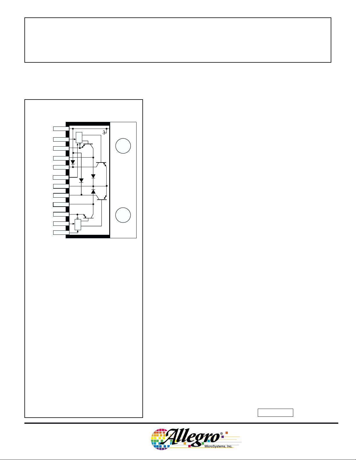
DUAL SOLENOID/MOTOR DRIVER
—PULSE-WIDTH MODULATED CURRENT CONTROL
Using PWM to minimize power dissipation and maximize load
efficiency, the UDN2962W dual driver is recommended for impact
printer solenoids and stepper motors. It is comprised of two source/
1
2
IN
A
A
43
A
5
A
6
A
7
CC
8
B
9
B
10
B
11
IN
B
12
B
LOGIC
LOGIC
Dwg. No. D-1001
sink driver pairs rated for continuous operation to ±3 A. It can be
connected to drive two independent loads or a single load in the fullbridge configuration. Both drivers include output clamp/flyback
diodes, input gain and level shifting, a voltage regulator for singlesupply operation, and pulse-width modulated output-current control
circuitry. Inputs are compatible with most TTL, DTL, LSTTL, and
low-voltage CMOS or PMOS logic.
The peak output current and hysteresis for each source/sink pair is
set independently. Output current, threshold voltage, and hysteresis are
set by the user’s selection of external resistors. At the specified outputcurrent trip level, the source driver turns off. The internal clamp diode
then allows current to flow without additional input from the power
supply. When the lower current trip point is reached, the source driver
turns back on.
The UDN2962W is in a 12-pin single in-line power-tab package.
The tab is at ground potential and needs no insulation. For highcurrent or high-frequency applications, external heat sinking may be
required.
29319.12A†
Data Sheet
ABSOLUTE MAXIMUM RATINGS
at TJ ≤ +150°C
Supply Voltage, VCC. . . . . . . . . . . . . . 45 V
Peak Output Current, I
Input Voltage Range,
. . . . . . . . . . . . . . . - 0.3 V to +7.0 V
V
IN
Package Power Dissipation,
. . . . . . . . . . . . . . . . . . . See Graph
P
D
Operating Temperature Range,
. . . . . . . . . . . . . . . . -20°C to +85°C
T
A
Storage Temperature Range,
. . . . . . . . . . . . . . . -55°C to +150°C
T
S
NOTE: Output current rating may be limited by
duty cycle, ambient temperature, and heat
sinking. Under any set of conditions, do not
exceed the specified peak current and a junction
temperature of +150°C.
. . . . . . . . . ±4 A
OUT
FEATURES
■ 4 A Peak Output
■ 45 V Min. Sustaining Voltage
■ Internal Clamp Diodes
■ TTL/PMOS/CMOS Compatible Inputs
■ High-Speed Chopper
Always order by complete part number: UDN2962W .
Page 2
2962
DUAL PWM
SOLENOID/MOTOR DRIVER
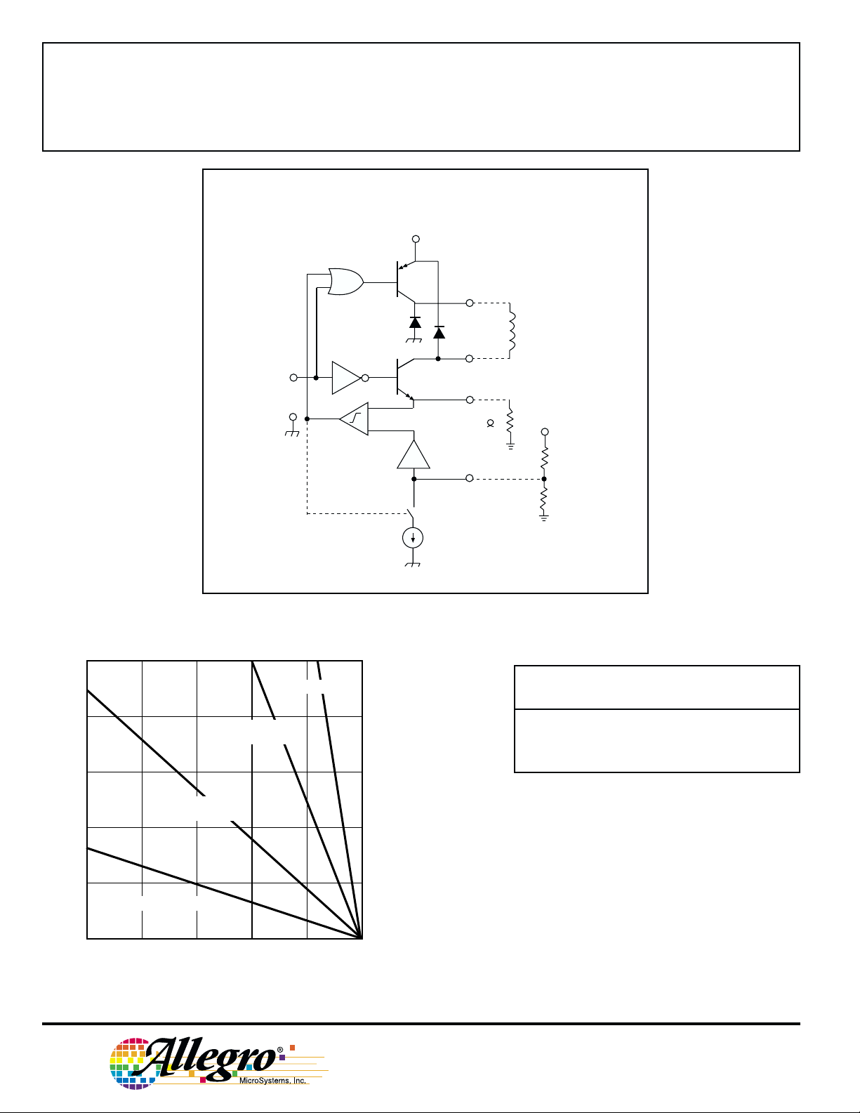
FUNCTIONAL BLOCK DIAGRAM
(ONE OF TWO DRIVERS)
IN
GND
+
_
-10
V
CC
SOURCE
SINK
SENSE
R
S
(TYP.0.1 )
THS
LOAD
V
REF
R
H
R
T
Dwg. No. D-1002
10
R = 2.0°C/W
θJT
8
3.0°C/W HEAT SINK
R = 5.0°C/W
θJA
V
IN
High NA Off Off
Low <V
Low >V
6
12°C/W HEAT SINK
R = 14°C/W
4
2
FREE AIR, R = 38°C/W
θJA
θJA
TRUTH TABLE
SOURCE SINK
V
SENSE
/10 On On
THS
/10 Off On
THS
DRIVER DRIVER
0
ALLOWABLE PACKAGE POWER DISSIPATION IN WATTS
25
50 75 100 125 150
TEMPERATURE IN °C
Dwg. GP-012B
115 Northeast Cutoff, Box 15036
W
Worcester, Massachusetts 01615-0036 (508) 853-5000
Copyright © 1986, 2000 Allegro MicroSystems, Inc.
Page 3
2962
DUAL PWM
SOLENOID/MOTOR DRIVER
ELECTRICAL CHARACTERISTICS at TA = +25°C, TJ ≤ +150°C, VCC = 45 V, V
otherwise noted).
= 0 V (unless
SENSE
Limits
Characteristic Symbol Test Conditions Min. Typ. Max. Units
Supply Voltage Range V
CC
Operating 20 — 45 V
Output Drivers
Output Leakage Current I
Output Saturation Voltage V
Output Sustaining Voltage V
CE(SAT)
CE(sus)
Output Current Regulation ∆I
Clamp Diode Forward Voltage V
Output Rise Time t
Output Fall Time t
CEX
OUT
F
r
f
V
= 2.4 V, V
IN
V
= 2.4 V, V
IN
Source Drivers, I
Source Drivers, I
Sink Drivers, I
Sink Drivers, I
I
= ±3.0 A, L = 3.5 mH 45 — — V
OUT
V
= 0.6 V to 1.0 V, L = 3.5 mH — — ±25 %
THS
V
= 1.0 V to 2.0 V, L = 3.5 mH — — ±10 %
THS
V
= 2.0 V to 5.0 V, L = 3.5 mH — — ±5.0 %
THS
= 0 V — <-1.0 -100 µA
SOURCE
= 45 V — <1.0 100 µA
SINK
= 3.0 A — 2.1 2.3 V
LOAD
= 1.0 A — 1.7 2.0 V
LOAD
= 3.0 A — 1.7 2.0 V
LOAD
= 1.0 A — 1.1 1.3 V
LOAD
IF = 3.0 A — 1.7 2.0 V
I
= 3.0 A, 10% to 90%, Resistive Load — 0.5 1.0 µs
LOAD
I
= 3.0 A, 90% to 10%, Resistive Load — 0.5 1.0 µs
LOAD
Control Logic
Logic Input Voltage V
Logic Input Current I
V
THS/VSENSE
Ratio — At Trip Point, V
Supply Current l
(Total Device)
Propagation Delay Time t
(Resistive Load)
* Where V
SENSE
≥ V
THS
/9.5
IN(1)
V
IN(0)
IN(1)
I
IN(0)
I
THS(ON)
I
THS(HYS)
CC
pd
VIN = 2.4 V — 1.0 10 µA
VIN = 0.8 V — -20 -100 µA
V
≥ 500 mV, V
THS
V
SENSE
≥ V
THS
/9.5, V
THS
≤ V
SENSE
THS
/10.5 — -2.0 — µA
THS
= 0.6 V to 5.0 V 140 200 260 µA
= 2.0 V to 5.0 V 9.5 10 10.5 —
VIN = 2.4 V, Outputs Off — 8.0 12 mA
V
= 0.8 V, Outputs Open — 25 40 mA
IN
50% VIN to 50% V
50% V
100% V
to 50% V
IN
SENSE
to 50% V
, Turn Off — — 2.5 µs
OUT
, Turn On — — 3.0 µs
OUT
* — — 3.0 µs
OUT
NOTE: Negative current is defined as coming out of (sourcing) the specified device pin.
2.4 — — V
— — 0.8 V
www.allegromicro.com
Page 4

2962
=
V
IN
V
SINK
V
SOURCE
I
LOAD
V
THS
V
CC
GND
V
CC
I
TRIP S THS
GND
RV
10
•
DUAL PWM
SOLENOID/MOTOR DRIVER
CIRCUIT DESCRIPTION
AND APPLICATIONS INFORMATION
The UDN2962W high-current driver is intended for use as a
free-running, pulse-width modulated solenoid driver.
Circuit Description. In operation, the source and sink drivers are
both turned on by a low level at the input. The load current rises with
time as a function of the load inductance, total circuit resistance, and
supply voltage and is sensed by the external sense resistor (RS).
When the load current reaches the trip point (I
), the comparator
TRIP
output goes high and turns off the source driver. The actual load
current will peak slightly higher than I
because of the internal logic
TRIP
and switching delays.
After the source driver is turned off, the load current continues to
circulate through the sink driver and an internal ground clamp diode.
The rate of current decay is a function of the load inductance and total
circuit resistance.
An internal constant current sink reduces the trip point (hysteresis)
until the decaying load current reaches the lower threshold, when the
comparator output goes low and the source driver is again turned on.
Load current is again allowed to rise to the trip point and the cycle
repeats.
Maximum load current and hysteresis is determined by the user.
Determining Maximum Load Current and Hysteresis. Trip
current (I
threshold voltage, V
) is determined as a function of resistance RS and the
TRIP
:
THS
V
=
THS
10 R
S
I
TRIP
Circuit Layout. To prevent interaction
between channels, each of the two high-level
power ground returns (the low side of the
sense resistors) must be returned independently to the low-level signal ground (pin 1).
The circuit common (pin 1) can then be
routed to the system ground.
The printed wiring board should utilize a
heavy ground plane. For optimum performance, the driver should be soldered directly
into the board.
The power supply (VCC) should be
decoupled with an electrolytic capacitor
(≥10 µF) as close as possible to pin 7.
SUPPLY
R
S
3 7
1
SYSTEM GROUND
+
R
S
10
Dwg. OP-001
TYPICAL WAVESHAPES
where V
= 10 x V
THS
= 0.6 V to 5.0 V.
SENSE
Hysteresis percentage (H) is determined by resistance RH and is
independent of the load current:
R
50 x V
H
REF
H =
The chopping frequency is asynchronous and a function of the
system and circuit parameters, including load inductance, supply
voltage, hysteresis setting, and switching speed of the driver.
Resistance RT is determined as:
RT =
Note that if V
THS
= V
REF,
RHV
THS
V
– V
REF
then RT = ∞.
THS
115 Northeast Cutoff, Box 15036
Worcester, Massachusetts 01615-0036 (508) 853-5000
Dwg. WP-006
Page 5

SOLENOID/MOTOR DRIVER
APPLICATIONS INFORMATION
2962
DUAL PWM
RESISTOR RH VALUE
AS A FUNCTION OF HYSTERESIS
25
20
kΩ
15
IN
H
R
10
5
0
0
20
V = 5 V
REF
40
HYSTERESIS, H, IN PERCENT
60
80 100
Dwg. No. A-12,417 Dwg. No. A-12,416
AS A FUNCTION OF PEAK LOAD CURRENT
25
20
kΩ
15
IN
T
R
10
5
0
0
RESISTOR RT VALUE
V = 5V
REF
R = 0.1Ω
S
0.5
1.0
1.5 2.0
LOAD CURRENT, I , IN AMPERES
MAX
2.5
H
3.0
5
2
=
H=20%
%
%
5
1
=
H
%
0
1
=
H
=5%
H
4.0
3.5
www.allegromicro.com
Dwg. No. D-1004
RH AND RT DETERMINE HYSTERESIS AND PEAK CURRENT
NOTE: Each of the drivers includes an internal logic delay to prevent
potentially destructive crossover currents within the driver during phase
changes. However, never simultaneously enable both inputs in the fullbridge configurations: A destructive short-circuit to ground will result.
Page 6

2962
DUAL PWM
SOLENOID/MOTOR DRIVER
Dimensions in Inches
(controlling dimensions)
INDEX
AREA
0.065
0.035
0.020
1.260
1.240
0.775
0.765
0.245
0.225
0.180
0.155
MAX
0.055
0.045
ø
0.145
0.140
0.135
0.100
0.365
0.570
0.540
0.290 MIN
1
0.030
0.020
12
0.100
±0.010
0.023
0.018
0.080
0.070
Dwg. MP-007 in
NOTES: 1. Lead thickness is measured at seating plane or below.
2. Lead spacing tolerance is non-cumulative.
3. Exact body and lead configuration at vendor’s option within limits shown.
4. Lead gauge plane is 0.030” below seating plane.
5. Supplied in standard sticks/tubes of 15 devices.
115 Northeast Cutoff, Box 15036
Worcester, Massachusetts 01615-0036 (508) 853-5000
Page 7

SOLENOID/MOTOR DRIVER
Dimensions in Millimeters
(for reference only)
2962
DUAL PWM
INDEX
AREA
1.65
0.89
0.51
1
32.00
31.49
19.69
19.45
0.76
0.51
12
6.22
5.71
3.56
9.27
2.54
±0.254
3.94
3.68
4.57
MAX
ø
14.48
13.71
7.36
MIN
0.59
0.45
1.40
1.14
3.43
2.54
2.03
1.77
NOTES: 1. Lead thickness is measured at seating plane or below.
2. Lead spacing tolerance is non-cumulative.
3. Exact body and lead configuration at vendor’s option within limits shown.
4. Lead gauge plane is 0.762 mm below seating plane.
5. Supplied in standard sticks/tubes of 15 devices.
The products described here are manufactured under one or more U.S.
patents or U.S. patents pending.
Allegro MicroSystems, Inc. reserves the right to make, from time to time,
such departures from the detail specifications as may be required to permit
improvements in the performance, reliability, or manufacturability of its
products. Before placing an order, the user is cautioned to verify that the
information being relied upon is current.
Allegro products are not authorized for use as critical components in lifesupport devices or systems without express written approval.
The information included herein is believed to be accurate and reliable.
However, Allegro MicroSystems, Inc. assumes no responsibility for its use; nor
for any infringement of patents or other rights of third parties which may result
from its use.
www.allegromicro.com
Dwg. MP-007 mm
Page 8

2962
DUAL PWM
SOLENOID/MOTOR DRIVER
MOTOR DRIVERS
Function Output Ratings* Part Number
INTEGRATED CIRCUITS FOR BRUSHLESS DC MOTORS
3-Phase Power MOSFET Controller — 28 V 3933
3-Phase Power MOSFET Controller — 50 V 3932
3-Phase Power MOSFET Controller — 50 V 7600
2-Phase Hall-Effect Sensor/Driver 400 mA 26 V 3626
Bidirectional 3-Phase Back-EMF Controller/Driver ±600 mA 14 V 8906
2-Phase Hall-Effect Sensor/Driver 900 mA 14 V 3625
3-Phase Back-EMF Controller/Driver ±900 mA 14 V 8902–A
3-Phase Controller/Drivers ±2.0 A 45 V 2936 & 2936-120
INTEGRATED BRIDGE DRIVERS FOR DC AND BIPOLAR STEPPER MOTORS
Dual Full Bridge with Protection & Diagnostics ±500 mA 30 V 3976
PWM Current-Controlled Dual Full Bridge ±650 mA 30 V 3966
PWM Current-Controlled Dual Full Bridge ±650 mA 30 V 3968
PWM Current-Controlled Dual Full Bridge ±750 mA 45 V 2916
PWM Current-Controlled Dual Full Bridge ±750 mA 45 V 2919
PWM Current-Controlled Dual Full Bridge ±750 mA 45 V 6219
PWM Current-Controlled Dual Full Bridge ±800 mA 33 V 3964
PWM Current-Controlled Full Bridge ±1.3 A 50 V 3953
PWM Current-Controlled Dual Full Bridge ±1.5 A 45 V 2917
PWM Current-Controlled Microstepping Full Bridge ±1.5 A 50 V 3955
PWM Current-Controlled Microstepping Full Bridge ±1.5 A 50 V 3957
PWM Current-Controlled Dual DMOS Full Bridge ±1.5 A 50 V 3972
Dual Full-Bridge Driver ±2.0 A 50 V 2998
PWM Current-Controlled Full Bridge ±2.0 A 50 V 3952
DMOS Full Bridge PWM Driver ±2.0 A 50 V 3958
Dual DMOS Full Bridge ±2.5 A 50 V 3971
UNIPOLAR STEPPER MOTOR & OTHER DRIVERS
Voice-Coil Motor Driver ±500 mA 6 V 8932–A
Voice-Coil Motor Driver ±800 mA 16 V 8958
Unipolar Stepper-Motor Quad Drivers 1 A 46 V 7024 & 7029
Unipolar Microstepper-Motor Quad Driver 1.2 A 46 V 7042
Unipolar Stepper-Motor Translator/Driver 1.25 A 50 V 5804
Unipolar Stepper-Motor Quad Driver 1.8 A 50 V 2540
Unipolar Stepper-Motor Quad Driver 1.8 A 50 V 2544
Unipolar Stepper-Motor Quad Driver 3 A 46 V 7026
Unipolar Microstepper-Motor Quad Driver 3 A 46 V 7044
* Current is maximum specified test condition, voltage is maximum rating. See specification for sustaining voltage limits or
over-current protection voltage limits. Negative current is defined as coming out of (sourcing) the output.
† Complete part number includes additional characters to indicate operating temperature range and package style.
Also, see 3175, 3177, 3235, and 3275 Hall-effect sensors for use with brushless dc motors.
†
115 Northeast Cutoff, Box 15036
Worcester, Massachusetts 01615-0036 (508) 853-5000
 Loading...